K6F1616U6C.fm
K6F1616U6C Family
Revision 2.0
May 2005
1
CMOS SRAM
* Samsung Electronics reserves the right to change products or specification without notice.
INFORMATION IN THIS DOCUMENT IS PROVIDED IN RELATION TO SAMSUNG PRODUCTS,
AND IS SUBJECT TO CHANGE WITHOUT NOTICE.
NOTHING IN THIS DOCUMENT SHALL BE CONSTRUED AS GRANTING ANY LICENSE,
EXPRESS OR IMPLIED, BY ESTOPPEL OR OTHERWISE, TO ANY INTELLECTUAL PROP-
ERTY RIGHTS IN SAMSUNG PRODUCTS OR TECHNOLOGY.
ALL INFORMATION IN THIS DOCUMENT IS PROVIDED ON AS "AS IS" BASIS WITHOUT
GUARANTEE OR WARRANTY OF ANY KIND.
1. For updates or additional information about Samsung products, contact your nearest Samsung office.
2. Samsung products are not intended for use in life support, critical care, medical, safety equipment, or simi-
lar applications where Product failure could result in loss of life or personal or physical harm, or any military
or defense application, or any governmental procurement to which special terms or provisions may apply.
16Mb(1M x 16 bit) Low Power SRAM
K6F1616U6C Family
Revision 2.0
May 2005
2
CMOS SRAM
Document Title
1M x16 bit Super Low Power and Low Voltage Full CMOS Static RAM
Revision History
Revision No.
0.0
1.0
2.0
Remark
Preliminary
Final
Final
History
Initial draft
Finalize
Revised
- Added Lead Free Products
Draft Date
November 14, 2003
March 31, 2005
May 11, 2005
The attached datasheets are provided by SAMSUNG Electronics. SAMSUNG Electronics CO., LTD. reserve the right to change the specifications and
products. SAMSUNG Electronics will answer to your questions about device. If you have any questions, please contact the SAMSUNG branch offices.
K6F1616U6C Family
Revision 2.0
May 2005
3
CMOS SRAM
1M x 16 bit Super Low Power and Low Voltage Full CMOS Static RAM
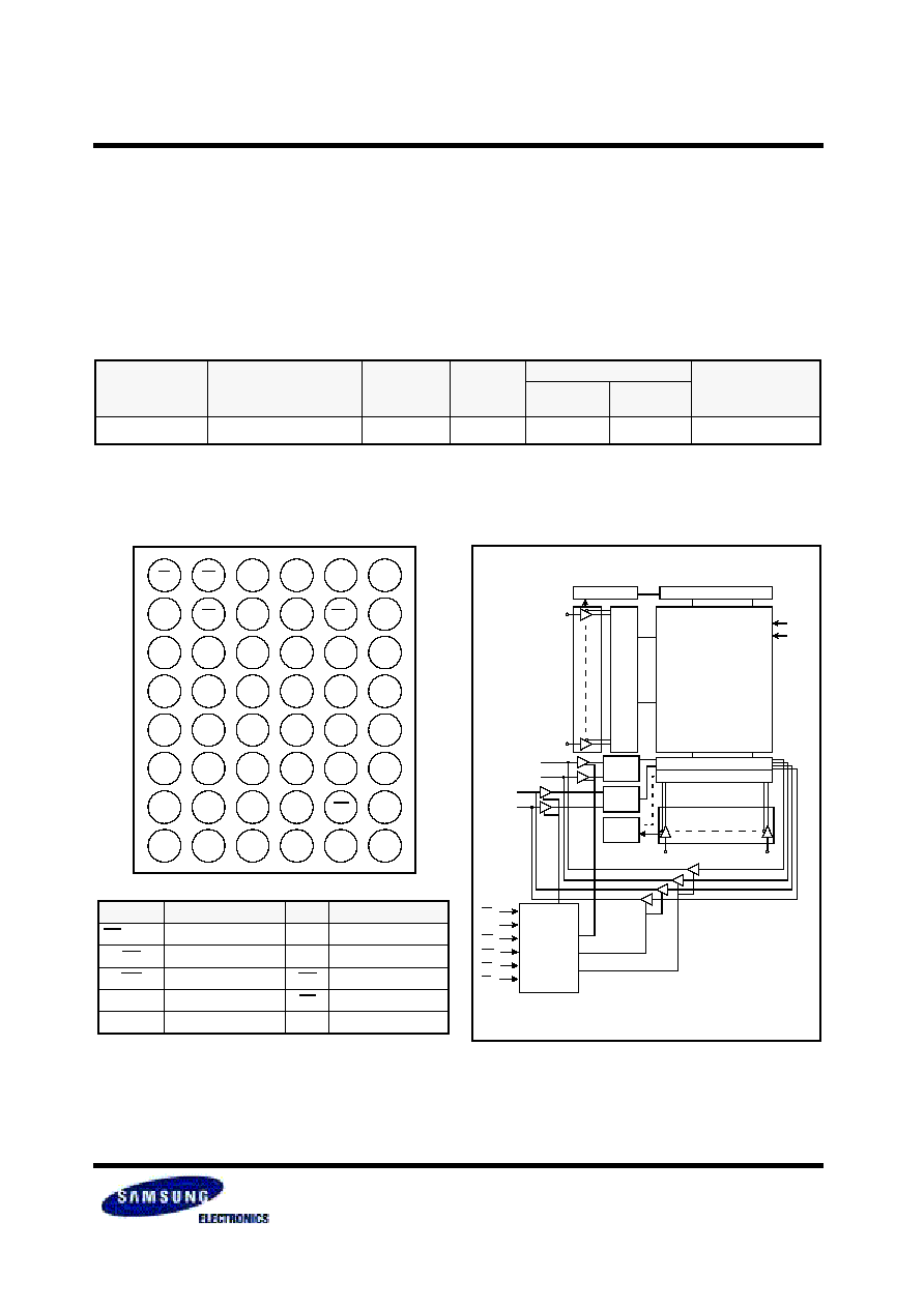
GENERAL DESCRIPTION
The K6F1616U6C families are fabricated by SAMSUNG
s
advanced full CMOS process technology. The families support
industrial operating temperature ranges. The families also sup-
port low data retention voltage for battery back-up operation
with low data retention current.
FEATURES
·
Process Technology: Full CMOS
·
Organization: 1M x16
·
Power Supply Voltage: 2.7~3.3V
·
Low Data Retention Voltage: 1.5V(Min)
·
Three State Outputs
·
Package Type: 48-FBGA - 6.00x7.00
Name
Function
Name
Function
CS1, CS2 Chip Select Inputs
Vcc
Power
OE
Output Enable Input
Vss
Ground
WE
Write Enable Input
UB
Upper Byte(I/O
9
~
16
)
A
0
~A
19
Address Inputs
LB
Lower Byte(I/O
1
~
8
)
I/O
1
~I/O
16
Data Inputs/Outputs
NC
No Connection
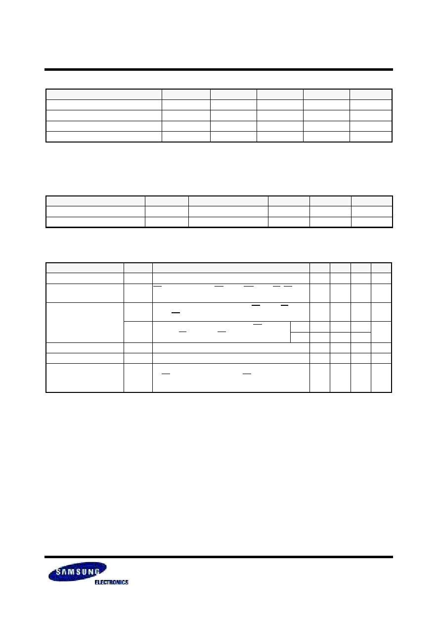
PRODUCT FAMILY
1. The parameter is measured with 30pF test load.
2. Typical value is measured at V
CC
=3.0V, T
A
=25
°
C and not 100% tested.
Product Family
Operating Temperature
Vcc Range
Speed
Power Dissipation
PKG Type
Standby
(I
SB1
, Typ.)
Operating
(I
CC1
, Max)
K6F1616U6C-F
Industrial(-40~85
°
C)
2.7~3.3V
55
1)
/70ns
5
µ
A
2)
5mA
48-FBGA - 6.00x7.00
SAMSUNG ELECTRONICS CO., LTD. reserves the right to change products and specifications without notice.
FUNCTIONAL BLOCK DIAGRAM
Clk gen.
Row
select
I/O
1
~I/O
8
Data
cont
Data
cont
Data
cont
I/O
9
~I/O
16
Vcc
Vss
Precharge circuit.
Memory
Cell
Array
I/O Circuit
Column select
PIN DESCRIPTION
WE
OE
UB
CS1
LB
Control Logic
CS2
Row
Addresses
Column Addresses
48-FBGA: Top View (Ball Down)
LB
OE
A0
A1
A2
CS2
I/O9
UB
A3
A4
CS1
I/O1
I/O10
I/O11
A5
A6
I/O2
I/O3
Vss
I/O12
A17
A7
I/O4
Vcc
Vcc
I/O13
NC
A16
I/O5
Vss
I/O15
I/O14
A14
A15
I/O6
I/O7
I/O16
A19
A12
A13
WE
I/O8
A18
A8
A9
A10
A11
NC
1
2
3
4
5
6
A
B
C
D
E
F
G
H
K6F1616U6C Family
Revision 2.0
May 2005
4
CMOS SRAM
PRODUCT LIST
1. LF : Lead Free Product
Industrial Temperature Products(-40~85
°
C)
Part Name
Function
K6F1616U6C-FF55
K6F1616U6C-XF55
K6F1616U6C-FF70
K6F1616U6C-XF70
48-FBGA, 55ns, 3.0V
48-FBGA, 55ns, 3.0V, LF
1)
48-FBGA, 70ns, 3.0V
48-FBGA, 70ns, 3.0V, LF
1)
ABSOLUTE MAXIMUM RATINGS
1)
1. Stresses greater than those listed under "Absolute Maximum Ratings" may cause permanent damage to the device. Functional operation should be
restricted to recommended operating condition. Exposure to absolute maximum rating conditions for extended periods may affect reliability.
Item
Symbol
Ratings
Unit
Voltage on any pin relative to Vss
V
IN
,V
OUT
-0.2 to V
CC
+0.3V(Max. 3.6V)
V
Voltage on Vcc supply relative to Vss
V
CC
-0.2 to 3.6
V
Power Dissipation
P
D
1.0
W
Storage temperature
T
STG
-65 to 150
°
C
Operating Temperature
T
A
-40 to 85
°
C
FUNCTIONAL DESCRIPTION
1. X means don
t care. (Must be low or high state)
CS
1
CS
2
OE
WE
LB
UB
I/O
1~8
I/O
9~16
Mode
Power
H
X
1)
X
1)
X
1)
X
1)
X
1)
High-Z
High-Z
Deselected
Standby
X
1)
L
X
1)
X
1)
X
1)
X
1)
High-Z
High-Z
Deselected
Standby
X
1)
X
1)
X
1)
X
1)
H
H
High-Z
High-Z
Deselected
Standby
L
H
H
H
L
X
1)
High-Z
High-Z
Output Disabled
Active
L
H
H
H
X
1)
L
High-Z
High-Z
Output Disabled
Active
L
H
L
H
L
H
Dout
High-Z
Lower Byte Read
Active
L
H
L
H
H
L
High-Z
Dout
Upper Byte Read
Active
L
H
L
H
L
L
Dout
Dout
Word Read
Active
L
H
X
1)
L
L
H
Din
High-Z
Lower Byte Write
Active
L
H
X
1)
L
H
L
High-Z
Din
Upper Byte Write
Active
L
H
X
1)
L
L
L
Din
Din
Word Write
Active
K6F1616U6C Family
Revision 2.0
May 2005
5
CMOS SRAM
RECOMMENDED DC OPERATING CONDITIONS
1)
Note:
1. T
A
=-40 to 85
°
C, otherwise specified
2. Overshoot: V
CC
+2.0V in case of pulse width
20ns.
3. Undershoot: -2.0V in case of pulse width
20ns.
4. Overshoot and Undershoot are sampled, not 100% tested.
Item
Symbol
Min
Typ
Max
Unit
Supply voltage
Vcc
2.7
3.0
3.3
V
Ground
Vss
0
0
0
V
Input high voltage
V
IH
2.2
-
Vcc+0.2
2)
V
Input low voltage
V
IL
-0.2
3)
-
0.6
V
CAPACITANCE
1)
(f=1MHz, T
A
=25
°
C)
1. Capacitance is sampled, not 100% tested
Item
Symbol
Test Condition
Min
Max
Unit
Input capacitance
C
IN
V
IN
=0V
-
8
pF
Input/Output capacitance
C
IO
V
IO
=0V
-
10
pF
DC AND OPERATING CHARACTERISTICS
1. Typical values are measured at V
CC
=3.0V, T
A
=25
°
C and not 100% tested.
Item
Symbol
Test Conditions
Min
Typ
1)
Max
Unit
Input leakage current
I
LI
V
IN
=Vss to Vcc
-1
-
1
µ
A
Output leakage current
I
LO
CS
1
=V
IH
or CS
2
=V
IL
or OE=V
IH
or WE=V
IL
or LB=UB=V
IH
,
V
IO
=Vss to Vcc
-1
-
1
µ
A
Average operating current
I
CC1
Cycle time=1
µ
s, 100%duty, I
IO
=0mA, CS
1
0.2V, LB
0.2V
or/and UB
0.2V, CS
2
Vcc-0.2V, V
IN
0.2V or V
IN
V
CC
-0.2V
-
-
5
mA
I
CC2
Cycle time=Min, I
IO
=0mA, 100% duty, CS
1
=V
IL
,
CS
2
=V
IH
, LB=V
IL
or/and UB=V
IL
, V
IN
=V
IL
or V
IH
70ns
-
-
25
mA
55ns
-
-
30
Output low voltage
V
OL
I
OL
= 2.1mA
-
-
0.4
V
Output high voltage
V
OH
I
OH
= -1.0mA
2.4
-
-
V
Standby Current (CMOS)
I
SB1
Other input =0~Vcc
1) CS
1
Vcc-0.2V, CS
2
Vcc-0.2V(CS
1
controlled) or
2) 0V
CS
2
0.2V(CS
2
controlled)
-
5.0
25
µ
A