K6R1016V1C-C/C-L, K6R1016V1C-I/C-P
CMOS SRAM
Revision 4.0
- 1 -
September 2001
for AT&T
Document Title
64Kx16 Bit High-Speed CMOS Static RAM(3.3V Operating)
Operated at Commercial and Industrial Temperature Ranges.
Revision History
The attached data sheets are prepared and approved by SAMSUNG Electronics. SAMSUNG Electronics CO., LTD. reserve the right to change the
specifications. SAMSUNG Electronics will evaluate and reply to your requests and questions on the parameters of this device. If you have any questions,
please contact the SAMSUNG branch office near your office, call or contact Headquarters.
Rev. No.
Rev. 0.0
Rev. 1.0
Rev. 2.0
Rev. 2.1
Rev. 2.2
Rev. 3.0
Rev. 3.1
Rev. 3.2
Rev. 3.3
Rev. 4.0
Remark
Preliminary
Final
Final
Final
Final
Final
Final
Final
Final
Final
History
Initial release with Preliminary.
Release to Final Data Sheet.
1.1. Delete Preliminary.
1.2. Changed DC characteristics.
Added 48-fine pitch BGA.
Changed device part name for FP-BGA.
ex) K6R1016V1C-Z -> K6R1016V1C-F
Changed device ball name for FP-BGA.
1. Added 10ns speed for FP-BGA only.
2. Changed Standby Current.
3. Added Data Retention Characteristics.
Added 10ns speed for all packages(44SOJ / 44TSOP2 / 48FPBGA)
Supply Voltage Change
1. Only 10ns Bin : 3.15V ~ 3.6V
2. The Rest Bin : 3.0V ~ 3.6V
V
IH
/V
IL
Change
Delete 20ns speed bin
Item
Previous
Changed
I
CC
12ns
85mA
95mA
15ns
83mA
93mA
20ns
80mA
90mA
Item
Previous
Changed
Symbol
Z
F
Previous
Changed
I/O1 ~ I/O8
I/O9 ~ I/O16
I/O9 ~ I/O16
I/O1 ~ I/O8
Item
Previous
Changed
Standby Current(Isb1)
0.3mA
0.5mA
Item
Previous
Changed
Min
Max
Min
Max
V
IH
2.0
V
CC
+0.5
2.0
V
CC
+0.3
V
IL
-0.5
0.8
-0.3
0.8
Draft Data
Aug. 5. 1998
Sep. 7. 1998
Sep. 17. 1998
Nov. 5. 1998
Dec. 10. 1998
Mar. 2. 1999
Apr. 24. 2000
Aug. 25. 2000
Oct. 2. 2000
Sep. 24. 2001
K6R1016V1C-C/C-L, K6R1016V1C-I/C-P
CMOS SRAM
Revision 4.0
- 2 -
September 2001
for AT&T
64K x 16 Bit High-Speed CMOS Static RAM(3.3V Operating)
The K6R1016V1C is a 1,048,576-bit high-speed Static Random
Access Memory organized as 65,536 words by 16 bits. The
K6R1016V1C uses 16 common input and output lines and has
at output enable pin which operates faster than address access
time at read cycle. Also it allows that lower and upper byte
access by data byte control (UB, LB). The device is fabricated
using SAMSUNG
s advanced CMOS process and designed for
high-speed circuit technology. It is particularly well suited for
use in high-density high-speed system applications. The
K6R1016V1C is packaged in a 400mil 44-pin plastic SOJ or
TSOP2 forward or 48-Fine pitch BGA.
GENERAL DESCRIPTION
FEATURES
� Fast Access Time 10,12,15ns(Max.)
� Low Power Dissipation
Standby (TTL) : 30mA(Max.)
(CMOS) : 5mA(Max.)
0.5mA(Max.) L-ver. only
Operating
*
K6R1016V1C-10: 105 mA(Max.)
K6R1016V1C-12: 95mA(Max.)
K6R1016V1C-15: 93mA(Max.)
� Single 3.3V Power Supply
� TTL Compatible Inputs and Outputs
� Fully Static Operation
- No Clock or Refresh required
� Three State Outputs
� 2V Minimum Data Retention: L-ver. only
� Center Power/Ground Pin Configuration
� Data Byte Control: LB: I/O
1
~ I/O
8
, UB: I/O
9
~ I/O
16
� Standard Pin Configuration:
K6R1016V1C-J: 44-SOJ-400
K6R1016V1C-T: 44-TSOP2-400BF
K6R1016V1C-F: 48-Fine pitch BGA with 0.75 Ball pitch
Clk Gen.
I/O
1
~I/O
8
OE
UB
CS
FUNCTIONAL BLOCK DIAGRAM
R
o
w
S
e
l
e
c
t
Data
Cont.
Column Select
A
10
A
11
A
12
A
13
A
14
A
15
CLK
Gen
.
Pre-Charge Circuit
Memory Array
512 Rows
128x16 Columns
I/O Circuit &
A
0
I/O
9
~I/O
16
Data
Cont.
WE
LB
K6R1016V1C-C10/C12/C15
Commercial Temp.
K6R1016V1C-I10/I12/I15
Industrial Temp.
ORDERING INFORMATION
A
1
A
2
A
3
A
4
A
5
A
6
A
7
A
9
A
8
PIN FUNCTION
Pin Name
Pin Function
A
0
- A
15
Address Inputs
WE
Write Enable
CS
Chip Select
OE
Output Enable
LB
Lower-byte Control(I/O
1
~I/O
8
)
UB
Upper-byte Control(I/O
9
~I/O
16
)
I/O
1
~ I/O
16
Data Inputs/Outputs
V
CC
Power(+3.3V)
V
SS
Ground
N.C
No Connection
K6R1016V1C-C/C-L, K6R1016V1C-I/C-P
CMOS SRAM
Revision 4.0
- 3 -
September 2001
for AT&T
ABSOLUTE MAXIMUM RATINGS*
* Stresses greater than those listed under "Absolute Maximum Ratings" may cause permanent damage to the device. This is a stress rating only and
functional operation of the device at these or any other conditions above those indicated in the operating sections of this specification is not implied.
Exposure to absolute maximum rating conditions for extended periods may affect reliability.
Parameter
Symbol
Rating
Unit
Voltage on Any Pin Relative to V
SS
V
IN
,
V
OUT
-0.5 to 4.6
V
Voltage on V
CC
Supply Relative to V
SS
V
CC
-0.5 to 4.6
V
Power Dissipation
P
d
1
W
Storage Temperature
T
STG
-65 to 150
�
C
Operating Temperature
Commercial
T
A
0 to 70
�
C
Industrial
T
A
-40 to 85
�
C
RECOMMENDED DC OPERATING CONDITIONS
(T
A
= 0 to 70
�
C)
(1) For K6R1016V1C-10 only.
(2) For all speed grades except K6R1016V1C-10.
(3) V
IH
(Max) = V
CC +
2.0V a.c(Pulse Width
8ns) for I
20mA
(4) V
IL
(Min) = -2.0V a.c(Pulse Width
8ns) for I
20mA.
Parameter
Symbol
Min
Typ
Max
Unit
Supply Voltage
V
CC
(1)
3.15
3.3
3.6
V
Supply Voltage
V
CC
(2)
3.0
3.3
3.6
V
Ground
V
SS
0
0
0
V
Input High Voltage
V
IH
2.0
-
V
CC
+0.3
(3)
V
Input Low Voltage
V
IL
-0.3
(4)
-
0.8
V
LB
OE
A0
A1
A2
N.C
I/O1
UB
A3
A4
CS
I/O9
I/O2
I/O3
A5
A6
I/O11
I/O10
Vss
I/O4
N.C
A7
I/O12
Vcc
Vcc
I/O5
N.C
N.C
I/O13
Vss
I/O7
I/O6
A14
A15
I/O14
I/O15
I/O8
N.C
A12
A13
WE
I/O16
N.C
A8
A9
A10
A11
N.C
1
2
3
4
5
6
A
B
C
D
E
F
G
H
48-CSP
PIN CONFIGURATION(TOP VIEW)
SOJ/
TSOP2
1
2
3
4
5
6
7
8
9
10
11
12
13
14
15
16
17
18
19
20
21
22
A
15
A
14
A
13
OE
UB
LB
I/O
16
I/O
15
I/O
14
I/O
13
Vss
Vcc
I/O
12
I/O
11
I/O
10
I/O
9
N.C
A
12
A
11
A
10
A
9
N.C
A
0
A
1
A
2
A
3
A
4
CS
I/O
1
I/O
2
I/O
3
I/O
4
Vcc
Vss
I/O
5
I/O
6
I/O
7
I/O
8
WE
A
5
A
6
A
7
A
8
N.C
44
43
42
41
40
39
38
37
36
35
34
33
32
31
30
29
28
27
26
25
24
23
K6R1016V1C-C/C-L, K6R1016V1C-I/C-P
CMOS SRAM
Revision 4.0
- 4 -
September 2001
for AT&T
TEST CONDITIONS*
* The above test conditions are also applied at industrial temperature range.
Parameter
Value
Input Pulse Levels
0V to 3V
Input Rise and Fall Times
3ns
Input and Output timing Reference Levels
1.5V
Output Loads
See below
AC CHARACTERISTICS
(T
A
=0 to 70
�
C, Vcc=3.3V+0.3V/-0.15V, unless otherwise noted.)
Output Loads(B)
D
OUT
5pF*
319
353
for t
HZ
, t
LZ
, t
WHZ
, t
OW
, t
OLZ
& t
OHZ
+3.3V
* Including Scope and Jig Capacitance
Output Loads(A)
D
OUT
R
L
= 50
Z
O
= 50
V
L
= 1.5V
30pF*
* Capacitive Load consists of all components of the
test environment.
CAPACITANCE*
(T
A
=25
�
C, f=1.0MHz)
* Capacitance is sampled and not 100% tested.
Item
Symbol
Test Conditions
MIN
Max
Unit
Input/Output Capacitance
C
I/O
V
I/O
=0V
-
8
pF
Input Capacitance
C
IN
V
IN
=0V
-
6
pF
*
DC AND OPERATING CHARACTERISTICS*
(
T
A
=0 to 70
�
C, Vcc=3.3V+0.3V/-0.15V, unless otherwise specfied)
* The above parameters are also guaranteed at industrial temperature range.
Parameter
Symbol
Test Conditions
Min
Max
Unit
Input Leakage Current
I
LI
V
IN
=V
SS
to
V
CC
-2
2
�
A
Output Leakage Current
I
LO
CS=V
IH
or OE =V
IH
or WE=V
IL
V
OUT
=V
SS
to
V
CC
-2
2
�
A
Operating Current
I
CC
Min. Cycle, 100% Duty
CS=V
IL,
V
IN
= V
IH
or
V
IL,
I
OUT
= 0mA
10ns
-
105
mA
12ns
-
95
15ns
-
93
Standby Current
I
SB
Min. Cycle, CS =V
IH
-
30
mA
I
SB1
f=0MHz, CS
V
CC
-0.2V,
V
IN
V
CC
-0.2V or V
IN
0.2V
Normal
-
5
mA
L-Ver.
-
0.5
Output Low Voltage Level
V
OL
I
OL
=8mA
-
0.4
V
Output High Voltage Level
V
OH
I
OH
=-4mA
2.4
-
V
K6R1016V1C-C/C-L, K6R1016V1C-I/C-P
CMOS SRAM
Revision 4.0
- 5 -
September 2001
for AT&T
WRITE CYCLE*
* The above parameters are also guaranteed at industrial temperature range.
Parameter
Symbol
K6R1016V1C-10
K6R1016V1C-12
K6R1016V1C-15
Unit
Min
Max
Min
Max
Min
Max
Write Cycle Time
t
WC
10
-
12
-
15
-
ns
Chip Select to End of Write
t
CW
7
-
8
-
9
-
ns
Address Set-up Time
t
AS
0
-
0
-
0
-
ns
Address Valid to End of Write
t
AW
7
-
8
-
9
-
ns
Write Pulse Width(OE High)
t
WP
7
-
8
-
9
-
ns
Write Pulse Width(OE Low)
t
WP1
10
-
12
-
15
-
ns
UB , LB Valid to End of Write
t
BW
7
-
8
-
9
-
ns
Write Recovery Time
t
WR
0
-
0
-
0
-
ns
Write to Output High-Z
t
WHZ
0
5
0
6
0
7
ns
Data to Write Time Overlap
t
DW
5
-
6
-
7
-
ns
Data Hold from Write Time
t
DH
0
-
0
-
0
-
ns
End Write to Output Low-Z
t
OW
3
-
3
-
3
-
ns
READ CYCLE*
* The above parameters are also guaranteed at industrial temperature range.
Parameter
Symbol
K6R1016V1C-10
K6R1016V1C-12
K6R1016V1C-15
Unit
Min
Max
Min
Max
Min
Max
Read Cycle Time
t
RC
10
-
12
-
15
-
ns
Address Access Time
t
AA
-
10
-
12
-
15
ns
Chip Select to Output
t
CO
-
10
-
12
-
15
ns
Output Enable to Valid Output
t
OE
-
5
-
6
-
7
ns
UB, LB Access Time
t
BA
-
5
-
6
-
7
ns
Chip Enable to Low-Z Output
t
LZ
3
-
3
-
3
-
ns
UB, LB Enable to Low-Z Output
t
BLZ
0
-
0
-
0
-
ns
Output Enable to Low-Z Output
t
OLZ
0
-
0
-
0
-
ns
Chip Disable to High-Z Output
t
HZ
0
5
0
6
-
7
ns
Output Disable to High-Z Output
t
OHZ
0
5
0
6
-
7
ns
UB, LB Disable to High-Z Output
t
BHZ
0
5
0
6
-
7
ns
Output Hold from Address Change
t
OH
3
-
3
-
3
-
ns
Chip Selection to Power Up Time
t
PU
0
-
0
-
0
-
ns
Chip Selection to Power DownTime
t
PD
-
10
-
12
-
15
ns
Address
Data Out
Previous Valid Data
Valid Data
TIMING DIAGRAMS
TIMING WAVEFORM OF READ CYCLE(1)
(Address Controlled
,
CS=OE=V
IL
, WE=V
IH
, UB, LB=V
IL
t
AA
t
RC
t
OH
K6R1016V1C-C/C-L, K6R1016V1C-I/C-P
CMOS SRAM
Revision 4.0
- 6 -
September 2001
for AT&T
NOTES(READ CYCLE)
1. WE is high for read cycle.
2. All read cycle timing is referenced from the last valid address to the first transition address.
3. t
HZ
and t
OHZ
are defined as the time at which the outputs achieve the open circuit condition and are not referenced to V
OH
or
V
OL
levels.
4. At any given temperature and voltage condition, t
HZ
(Max.) is less than t
LZ
(Min.) both for a given device and from device to
device.
5. Transition is measured
�
200mV from steady state voltage with Load(B). This parameter is sampled and not 100% tested.
6. Device is continuously selected with CS=V
IL.
7. Address valid prior to coincident with CS transition low.
8. For common I/O applications, minimization or elimination of bus contention conditions is necessary during read and write cycle.
TIMING WAVEFORM OF READ CYCLE(2)
(WE=V
IH
)
Valid Data
High-Z
t
RC
CS
Address
UB, LB
OE
Data out
t
HZ(3,4,5)
t
AA
t
CO
t
BA
t
OE
t
OLZ
t
LZ(4,5)
t
OH
t
OHZ
t
BHZ(3,4,5)
t
BLZ(4,5)
t
PU
t
PD
50%
50%
V
CC
Current
I
CC
I
SB
TIMING WAVEFORM OF WRITE CYCLE(1)
(OE =Clock)
Address
CS
UB, LB
WE
Data in
Data out
t
WC
t
CW(3)
t
BW
t
WP(2)
t
AS(4)
t
DH
t
DW
t
OHZ(6)
High-Z
High-Z
Valid Data
OE
t
AW
t
WR(5)
K6R1016V1C-C/C-L, K6R1016V1C-I/C-P
CMOS SRAM
Revision 4.0
- 7 -
September 2001
for AT&T
TIMING WAVEFORM OF WRITE CYCLE(3)
(CS=Controlled)
Address
CS
t
AW
t
DW
t
DH
Valid Data
WE
Data in
Data out
High-Z
High-Z(8)
UB, LB
t
CW(3)
t
WP(2)
t
AS(4)
t
WC
t
WR(5)
High-Z
High-Z
t
LZ
t
WHZ(6)
t
BW
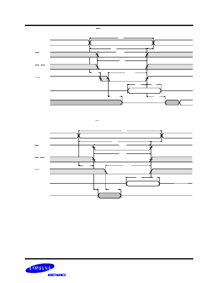
TIMING WAVEFORM OF WRITE CYCLE(2)
(OE =Low fixed)
Address
CS
UB, LB
WE
Data in
Data out
t
WC
t
CW(3)
t
BW
t
WP1(2)
t
DH
t
DW
t
WR(5)
t
AS(4)
t
OW
t
WHZ(6)
(10)
(9)
High-Z
Valid Data
t
AW
High-Z
K6R1016V1C-C/C-L, K6R1016V1C-I/C-P
CMOS SRAM
Revision 4.0
- 8 -
September 2001
for AT&T
FUNCTIONAL DESCRIPTION
* X means Don
t Care
.
CS
WE
OE
LB
UB
Mode
I/O Pin
Supply Current
I/O
1
~I/O
8
I/O
9
~I/O
16
H
X
X*
X
X
Not Select
High-Z
High-Z
I
SB
, I
SB1
L
H
H
X
X
Output Disable
High-Z
High-Z
I
CC
L
X
X
H
H
L
H
L
L
H
Read
D
OUT
High-Z
I
CC
H
L
High-Z
D
OUT
L
L
D
OUT
D
OUT
L
L
X
L
H
Write
D
IN
High-Z
I
CC
H
L
High-Z
D
IN
L
L
D
IN
D
IN
NOTES(WRITE CYCLE)
1. All write cycle timing is referenced from the last valid address to the first transition address.
2. A write occurs during the overlap of a low CS, WE, LB and UB. A write begins at the latest transition CS going low and WE
going low; A write ends at the earliest transition CS going high or WE going high. t
WP
is measured from the beginning of write
to the end of write.
3. t
CW
is measured from the later of CS going low to end of write.
4. t
A S
is measured from the address valid to the beginning of write.
5. t
W R
is measured from the end of write to the address change. t
WR
applied in case a write ends as CS or WE going high.
6. If OE, CS and WE are in the Read Mode during this period, the I/O pins are in the output low-Z state. Inputs of opposite phase
of the output must not be applied because bus contention can occur.
7. For common I/O applications, minimization or elimination of bus contention conditions is necessary during read and write cycle.
8. If CS goes low simultaneously with WE going or after WE going low, the outputs remain high impedance state.
9. Dout is the read data of the new address.
10. When CS is low: I/O pins are in the output state. The input signals in the opposite phase leading to the output should not be
applied.
Address
CS
Valid Data
UB, LB
WE
Data in
Data out
TIMING WAVEFORM OF WRITE CYCLE(4)
(UB, LB Controlled)
t
WC
t
CW(3)
t
BW
t
WP(2)
t
DH
t
DW
t
WR(5)
t
AW
t
AS(4)
High-Z
High-Z(8)
t
BLZ
t
WHZ(6)
High-Z

K6R1016V1C-C/C-L, K6R1016V1C-I/C-P
CMOS SRAM
Revision 4.0
- 9 -
September 2001
for AT&T
DATA RETENTION CHARACTERISTICS*
(T
A
=0
to 70
�
C)
* The above parameters are also guaranteed at industrial temperature range.
Data Retention Characteristic is for L-ver only.
Parameter
Symbol
Test Condition
Min.
Typ.
Max.
Unit
V
CC
for Data Retention
V
DR
CS
V
CC
-0.2V
2.0
-
3.6
V
Data Retention Current
I
DR
V
CC
=3.0V, CS
V
CC
-0.2V
V
IN
V
CC
-0.2V or V
IN
0.2V
-
-
0.4
mA
V
CC
=2.0V, CS
V
CC
-0.2V
V
IN
V
CC
-0.2V or V
IN
0.2V
-
-
0.3
Data Retention Set-Up Time
t
SDR
See Data Retention
Wave form(below)
0
-
-
ns
Recovery Time
t
RDR
5
-
-
ms
DATA RETENTION WAVE FORM
CS controlled
V
CC
3.0V
V
IH
V
DR
CS
GND
Data Retention Mode
CS
V
CC
- 0.2V
t
SDR
t
RDR

K6R1016V1C-C/C-L, K6R1016V1C-I/C-P
CMOS SRAM
Revision 4.0
- 10
September 2001
for AT&T
#1
44-SOJ-400
#44
25.58
�
0.12
1.125
�
0.005
MAX
28.98
1.141
MAX
0.148
3.76
1.19
( )
0.047
1.27
( )
0.050
0.95
( )
0.0375
+0.10
0.43
- 0.05
+0.004
0.017
-0.002
+0.10
0.71
-0.05
+0.004
0.028
-0.002
1.27
0.050
1
0
.
1
6
0
.
4
0
0
+0.10
0.20
-0.05
+0.004
0.008
-0.002
9.40
�
0.25
0.370
�
0.010
MIN
0.69
0.027
#22
#23
0.004
0.10 MAX
11.18
�
0.12
0.440
�
0.005
PACKAGE DIMENSIONS
Units:millimeters/Inches
1.00
�
0.10
0.039
�
0.004
44-TSOP2-400BF
0.002
#1
0.05
#22
#23
0.30
0.012
0.80
0.0315
MIN
0.047
1.20
MAX
0.741
18.81 MAX
18.41
�
0.10
0.725
�
0.004
11.76
�
0.20
0.463
�
0.008
+ 0.075
- 0.035
0.50
+ 0.003
- 0.001
0.125
0.005
0.020
1
0
.
1
6
0
.
4
0
0
0.10
0.004
0~8
�
0.45 ~0.75
0.018 ~ 0.030
( )
0.805
0.032
( )
MAX
Units:millimeters/Inches
#44
0.25
0.010 TYP
+
0.10
-
0.05
+
0.004
-
0.002
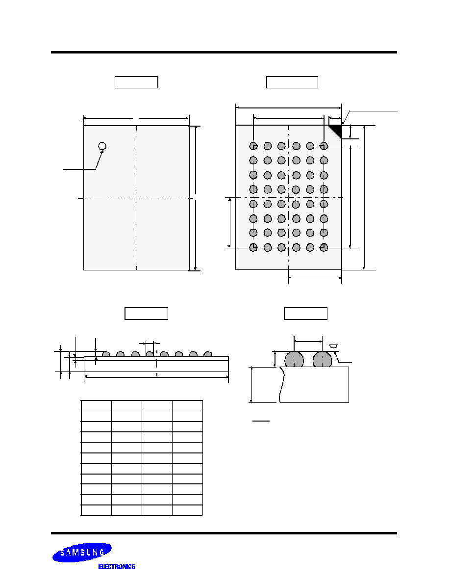
K6R1016V1C-C/C-L, K6R1016V1C-I/C-P
CMOS SRAM
Revision 4.0
- 11
September 2001
for AT&T
C
1
/
2
PACKAGE OUTLINE
(Units : millimeter)
6
5
4
3
2
1
A
B
C
D
E
F
G
H
C
B/2
B
C
1
B
C
Bottom View
Top View
D
E
2
E
1
E
C
Side View
0
.
8
0
/
T
y
p
.
0
.
2
5
/
T
y
p
.
A
Y
Detail A
Min
Typ
Max
A
-
0.75
-
B
5.90
6.00
6.10
B1
-
3.75
-
C
6.90
7.00
7.10
C1
-
5.25
-
D
0.30
0.35
0.40
E
-
1.05
1.20
E1
-
0.80
-
E2
0.20
0.25
0.30
Y
-
-
0.08
0.50
0.50
B1
#A1
0
.
3
0
A1 INDEX MARK
Notes.
1. Bump counts: 48(8row x 6column)
2. Bump pitch: (x,y)=(0.75 x 0.75)(typ.)
3. All tolerance are +/-0.050 unless
otherwise specified.
4. Typ: Typical
5. Y is coplanarity: 0.08(Max)