K6T1008V2C, K6T1008U2C Family
CMOS SRAM
Revision 2.0
November 1997
1
Document Title
128K x8 bit Low Power and Low Voltage CMOS Static RAM
Revision History
Remark
Preliminary
Final
Final
History
Initial draft
Finalize
- Increased I
SB
, I
DR
Commercial part = 10
µ
A
Industrial part = 20
µ
A
Revise
- Change speed bin
KM68V1000C Family: 70/85ns
70/100ns
KM68U1000C Family: 70/100ns
85/100ns
- Improved operating current: 40mA
35mA
- Improved power dissipation
P
D
: 0.7W
1.0W
- Improved standby current
Extended/Industrial: 20
10
µ
A
- VIL: 0.4V
0.6V
Draft Data
July 3, 1996
December 16, 1996
November 25, 1997
The attached datasheets are provided by SAMSUNG Electronics. SAMSUNG Electronics CO., LTD. reserves the right to change the specifications and
products. SAMSUNG Electronics will answer to your questions about device. If you have any questions, please contact the SAMSUNG branch offices.
Revision No.
0.0
1.0
2.0
K6T1008V2C, K6T1008U2C Family
CMOS SRAM
Revision 2.0
November 1997
2
128K x8 bit Low Power and Low Voltage CMOS Static RAM
GENERAL DESCRIPTION
The K6T1008V2C and K6T1008U2C families are fabricated by
SAMSUNG
s advanced CMOS process technology. The fami-
lies support various operating temperature ranges and have
various package types for user flexibility of system design. The
families also supports low data retention voltage for battery
back-up operation with low data retention current.
FEATURES
∑
Process Technology: 0.4
µ
m CMOS
∑
Organization: 128K x8
∑
Power Supply Voltage:
K6T1008V2C family: 3.0~3.6V
K6T1008U2C family: 2.7~3.3V
∑
Low Data Retention Voltage: 2V(Min)
∑
Three state output and TTL Compatible
∑
Package Type: 32-SOP-525, 32-TSOP1-0820F/R,
32-TSOP1-0813.4F/R
Name
Function
CS
1
, CS
2
Chip Select Inputs
OE
Output Enable Input
WE
Write Enable Input
A
0
~A
16
Address Inputs
I/O
1
~I/O
8
Data Inputs/Outputs
Vcc
Power
Vss
Ground
N.C
No Connection
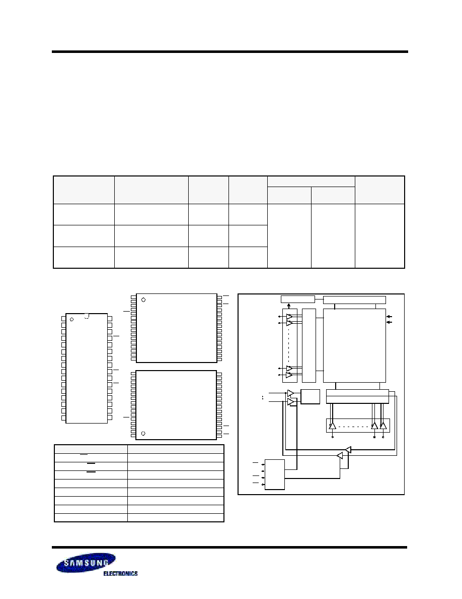
PRODUCT FAMILY
Product Family
Operating Temperature
Vcc Range
Speed
Power Dissipation
PKG Type
Standby
(I
SB1
, Max)
Operating
(I
CC2
, Max)
K6T1008V2C-B
Commercial(0~70
∞
C)
3.0~3.6V
70/100ns
10
µ
A
35mA
32-SOP
32-TSOP1-F/R
32-sTSOP1-F/R
K6T1008U2C-B
2.7~3.3V
85/100ns
K6T1008V2C-D
Extended(-25~85
∞
C)
3.0~3.6V
70/100ns
K6T1008U2C-D
2.7~3.3V
85/100ns
K6T1008V2C-F
Industrial(-40~85
∞
C)
3.0~3.6V
70/100ns
K6T1008U2C-F
2.7~3.3V
85/100ns
FUNCTIONAL BLOCK DIAGRAM
PIN DESCRIPTION
32-TSOP
Type1-Reverse
A11
A9
A8
A13
WE
CS2
A15
VCC
NC
A16
A14
A12
A7
A6
A5
A4
OE
A10
CS1
I/O8
I/O7
I/O6
I/O5
I/O4
VSS
I/O3
I/O2
I/O1
A0
A1
A2
A3
32-
S
TSOP
Type1-Forward
32
31
30
29
28
27
26
25
24
23
22
21
20
19
18
17
1
2
3
4
5
6
7
8
9
10
11
12
13
14
15
16
N.C
A16
A14
A12
A7
A6
A5
A4
A3
A2
A1
A0
I/O1
I/O2
I/O3
VSS
VCC
A15
CS2
WE
A13
A8
A9
A11
OE
A10
CS1
I/O8
I/O7
I/O6
I/O5
I/O4
32
31
30
29
28
27
26
25
24
23
22
21
20
19
18
17
1
2
3
4
5
6
7
8
9
10
11
12
13
14
15
16
32-SOP
A11
A9
A8
WE
A13
CS2
VCC
A15
NC
A16
A14
A12
A7
A6
A5
A4
OE
A10
CS1
I/O8
I/O7
I/O6
I/O5
I/O4
VSS
I/O3
I/O2
I/O1
A0
A1
A2
A3
32
31
30
29
28
27
26
25
24
23
22
21
20
19
18
17
1
2
3
4
5
6
7
8
9
10
11
12
13
14
15
16
32-TSOP
SAMSUNG ELECTRONICS CO., LTD. reserves the right to change products and specifications without notice.
Precharge circuit.
Memory array
1024 rows
128
◊
8 columns
I/O Circuit
Column select
Clk gen.
Row
select
A10 A0
A1
A2
A3
A11
A9
I/O
1
Data
cont
I/O
8
V
CC
V
SS
A4
A5
A6
A7
A8
A12
A14
A13
A15
A16
CS1
WE
OE
Control
logic
CS2
32-
S
TSOP

K6T1008V2C, K6T1008U2C Family
CMOS SRAM
Revision 2.0
November 1997
3
PRODUCT LIST
Commercial Temperature Products
(0~70
∞
C)
Extended Temperature Products
(-25~85
∞
C)
Industrial Temperature Products
(-40~85
∞
C)
Part Name
Function
Part Name
Function
Part Name
Function
K6T1008V2C-GB70
K6T1008V2C-GB10
K6T1008V2C-TB70
K6T1008V2C-TB10
K6T1008V2C-RB70
K6T1008V2C-RB10
K6T1008U2C-GB85
K6T1008U2C-GB10
K6T1008U2C-TB85
K6T1008U2C-TB10
K6T1008U2C-RB85
K6T1008U2C-RB10
K6T1008V2C-YB70
K6T1008V2C-YB10
K6T1008V2C-NB70
K6T1008V2C-NB10
K6T1008U2C-YB85
K6T1008U2C-YB10
K6T1008U2C-NB85
K6T1008U2C-NB10
32-SOP, 70ns, 3.3V
32-SOP, 100ns, 3.3V
32-TSOP F, 70ns, 3.3V
32-TSOP F, 100ns, 3.3V
32-TSOP R, 70ns, 3.3V
32-TSOP R, 100ns, 3.3V
32-SOP, 85ns, 3.0V
32-SOP, 100ns, 3.0V
32-TSOP F, 85ns, 3.0V
32-TSOP F, 100ns, 3.0V
32-TSOP R, 85ns, 3.0V
32-TSOP R, 100ns, 3.0V
32-sTSOP F, 70ns, 3.3V
32-sTSOP F, 100ns, 3.3V
32-sTSOP R, 70ns, 3.3V
32-sTSOP R, 100ns, 3.3V
32-sTSOP F, 85ns, 3.0V
32-sTSOP F, 100ns, 3.0V
32-sTSOP R, 85ns, 3.0V
32-sTSOP R, 100ns, 3.0V
K6T1008V2C-GD70
K6T1008V2C-GD10
K6T1008V2C-TD70
K6T1008V2C-TD10
K6T1008V2C-RD70
K6T1008V2C-RD10
K6T1008U2C-GD85
K6T1008U2C-GD10
K6T1008U2C-TD85
K6T1008U2C-TD10
K6T1008U2C-RD85
K6T1008U2C-RD10
K6T1008V2C-YD70
K6T1008V2C-YD10
K6T1008V2C-ND70
K6T1008V2C-ND10
K6T1008U2C-YD85
K6T1008U2C-YD10
K6T1008U2C-ND85
K6T1008U2C-ND10
32-SOP, 70ns, 3.3V
32-SOP, 100ns, 3.3V
32-TSOP F, 70ns, 3.3V
32-TSOP F, 100ns, 3.3V
32-TSOP R, 70ns, 3.3V
32-TSOP R, 100ns, 3.3V
32-SOP, 85ns, 3.0V
32-SOP, 100ns, 3.0V
32-TSOP F, 85ns, 3.0V
32-TSOP F, 100ns, 3.0V
32-TSOP R, 85ns, 3.0V
32-TSOP R, 100ns, 3.0V
32-sTSOP F, 70ns, 3.3V
32-sTSOP F, 100ns, 3.3V
32-sTSOP R, 70ns, 3.3V
32-sTSOP R, 100ns, 3.3V
32-sTSOP F, 85ns, 3.0V
32-sTSOP F, 100ns, 3.0V
32-sTSOP R, 85ns, 3.0V
32-sTSOP R, 100ns, 3.0V
K6T1008V2C-GF70
K6T1008V2C-GF10
K6T1008V2C-TF70
K6T1008V2C-TF10
K6T1008V2C-RF70
K6T1008V2C-RF10
K6T1008U2C-GF85
K6T1008U2C-GF10
K6T1008U2C-TF85
K6T1008U2C-TF10
K6T1008U2C-RF85
K6T1008U2C-RF10
K6T1008V2C-YF70
K6T1008V2C-YF10
K6T1008V2C-NF70
K6T1008V2C-NF10
K6T1008U2C-YF85
K6T1008U2C-YF10
K6T1008U2C-NF85
K6T1008U2C-NF10
32-SOP, 70ns, 3.3V
32-SOP, 100ns, 3.3V
32-TSOP F, 70ns, 3.3V
32-TSOP F, 100ns, 3.3V
32-TSOP R, 70ns, 3.3V
32-TSOP R, 100ns, 3.3V
32-SOP, 85ns, 3.0V
32-SOP, 100ns, 3.0V
32-TSOP F, 85ns, 3.0V
32-TSOP F, 100ns, 3.0V
32-TSOP R, 85ns, 3.0V
32-TSOP R, 100ns, 3.0V
32-sTSOP F, 70ns, 3.3V
32-sTSOP F, 100ns, 3.3V
32-sTSOP R, 70ns, 3.3V
32-sTSOP R, 100ns, 3.3V
32-sTSOP F, 85ns, 3.0V
32-sTSOP F, 100ns, 3.0V
32-sTSOP R, 85ns, 3.0V
32-sTSOP R, 100ns, 3.0V
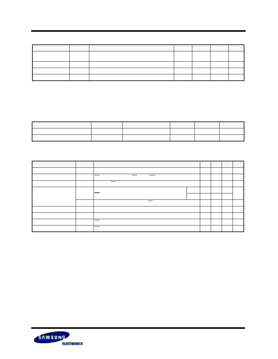
FUNCTIONAL DESCRIPTION
1. X means don
t care(Must be in high or low status.)
CS
1
CS
2
OE
WE
I/O
Pin
Mode
Power
H
X
1)
X
1)
X
1)
High-Z
Deselected
Standby
X
1)
L
X
1)
X
1)
High-Z
Deselected
Standby
L
H
H
H
High-Z
Output Disabled
Active
L
H
L
H
Dout
Read
Active
L
H
X
1)
L
Din
Write
Active
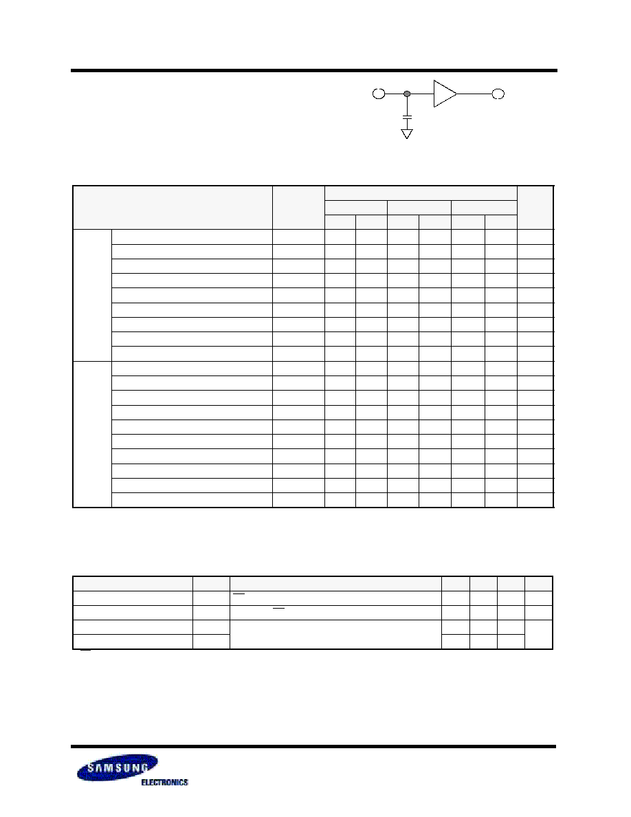
ABSOLUTE MAXIMUM RATINGS
1)
1. Stresses greater than those listed under "Absolute Maximum Ratings" may cause permanent damage to the device. Functional operation should be
restricted to recommended operating condition. Exposure to absolute maximum rating conditions for extended periods may affect reliability.
Item
Symbol
Ratings
Unit
Remark
Voltage on any pin relative to Vss
V
IN
,V
OUT
-0.5 to V
CC
+0.5
V
-
Voltage on Vcc supply relative to
V
CC
-0.3 to 4.6
V
-
Power Dissipation
P
D
1.0
W
-
Storage temperature
T
STG
-65 to 150
∞
C
-
Operating Temperature
T
A
0 to 70
∞
C
K6T1008V2C-B/K6T1008U2C-B
-25 to 85
∞
C
K6T1008V2C-D/K6T1008U2C-D
-40 to 85
∞
C
K6T1008V2C-F/K6T1008U2C-F
Soldering temperature and time
T
SOLDER
260
∞
C, 10sec (Lead Only)
-
-
K6T1008V2C, K6T1008U2C Family
CMOS SRAM
Revision 2.0
November 1997
4
CAPACITANCE
1)
(f=1MHz, TA=25
∞
C)
1
. Capacitance is sampled, not 100% tested
Item
Symbol
Test Condition
Min
Max
Unit
Input capacitance
C
IN
V
IN
=0V
-
6
pF
Input/Output capacitance
C
IO
V
IO
=0V
-
8
pF
RECOMMENDED DC OPERATING CONDITIONS
1)
1. Commercial Product: T
A
=0 to 70
∞
C, unless otherwise specified
Extended Product: T
A
=-25 to 85
∞
C, unless otherwise specified
Industrial Product: T
A
=-40 to 85
∞
C, unless otherwise specified
2. Overshoot: V
CC
+3.0V in case of pulse width
30ns
3. Undershoot: -3.0V in case of pulse width
30ns
4. Overshoot and undershoot is sampled, not 100% tested.
Item
Symbol
Product
Min
Typ
Max
Unit
Supply voltage
Vcc
K6T1008V2C Family
K6T1008U2C Family
3.0
2.7
3.3
3.0
3.6
3.3
V
Ground
Vss
All Family
0
0
0
V
Input high voltage
V
IH
K6T1008V2C, K6T1008U2C Family
2.2
-
Vcc+0.3
2)
V
Input low voltage
V
IL
K6T1008V2C, K6T1008U2C Family
-0.3
3)
-
0.6
V
DC AND OPERATING CHARACTERISTICS
Item
Symbol
Test Conditions
Min
Typ
Max
Unit
Input leakage current
I
LI
V
IN
=Vss to Vcc
-1
-
1
µ
A
Output leakage current
I
LO
CS
1
=V
IH
or CS
2
=V
IL
or OE=V
IH
or WE=V
IL,
V
IO
=Vss to Vcc
-1
-
1
µ
A
Operating power supply
I
CC
I
IO
=0mA, CS
1
=V
IL
, CS
2
=V
IH
, V
IN
=V
IL
or V
IH
, Read
-
2
5
mA
Average operating current
I
CC1
Cycle time=1
µ
s, 100% duty, I
IO
=0mA,
CS
1
0.2V, CS
2
V
CC
-0.2V, V
IN
0.2V or V
IN
V
CC
-0.2V
Read
-
1.5
5
mA
Write
10
15
I
CC2
Cycle time=Min, 100% duty, I
IO
=0mA, CS
1
=V
IL
, CS
2
=V
IH
, V
IN
=V
IL
or V
IH
-
25
35
mA
Output low voltage
V
OL
I
OL
=2.1mA
-
-
0.4
V
Output high voltage
V
OH
I
OH
=-1.0mA
2.2
-
-
V
Standby Current(TTL)
I
SB
CS
1
=V
IH,
CS
2
=V
IL
,
Other inputs=V
IL
or V
IH
-
-
0.3
mA
Standby Current(CMOS)
I
SB1
CS
1
Vcc-0.2V, CS
2
Vcc-0.2V or CS
2
0.2V, Other inputs=0~Vcc
-
0.3
10
µ
A
K6T1008V2C, K6T1008U2C Family
CMOS SRAM
Revision 2.0
November 1997
5
C
L
1)
1. Including scope and jig capacitance
AC OPERATING CONDITIONS
TEST CONDITIONS
(Test Load and Input/Output Reference)
Input pulse level: 0.4 to 2.2V
Input rising and falling time: 5ns
Input and output reference voltage:1.5V
Output load(see right): C
L
=100pF+1TTL
AC CHARACTERISTICS
(Commercial product:T
A
=0 to 70
∞
C, Extended product:T
A
=-25 to 85
∞
C, Industrial product: T
A
=-40 to 85
∞
C
K6T1008V2C Family: Vcc=3.0~3.6V, K6T1008U2C Family: Vcc=2.7~3.3V)
Parameter List
Symbol
Speed Bins
Units
70ns
85ns
100ns
Min
Max
Min
Max
Min
Max
Read
Read cycle time
t
RC
70
-
85
-
100
-
ns
Address access time
t
AA
-
70
-
85
-
100
ns
Chip select to output
t
CO1
, t
CO2
-
70
-
85
-
100
ns
Output enable to valid output
t
OE
-
35
-
40
-
50
ns
Chip select to low-Z output
t
LZ
10
-
10
-
10
-
ns
Output enable to low-Z output
t
OLZ
5
-
5
-
5
-
ns
Chip disable to high-Z output
t
HZ
0
25
0
25
0
30
ns
Output disable to high-Z output
t
OHZ
0
25
0
25
0
30
ns
Output hold from address change
t
OH
10
-
15
-
15
-
ns
Write
Write cycle time
t
WC
70
-
85
-
100
-
ns
Chip select to end of write
t
CW
60
-
70
-
80
-
ns
Address set-up time
t
AS
0
-
0
-
0
-
ns
Address valid to end of write
t
AW
60
-
70
-
80
-
ns
Write pulse width
t
WP
55
-
60
-
70
-
ns
Write recovery time
t
WR
0
-
0
-
0
-
ns
Write to output high-Z
t
WHZ
0
25
0
30
0
30
ns
Data to write time overlap
t
DW
30
-
35
-
40
-
ns
Data hold from write time
t
DH
0
-
0
-
0
-
ns
End write to output low-Z
t
OW
5
-
5
-
5
-
ns
DATA RETENTION CHARACTERISTICS
1. CS
1
Vcc-0.2V
,
CS
2
V
CC
-0.2V, or CS
2
0.2V
Item
Symbol
Test Condition
1)
Min
Typ
Max
Unit
Vcc for data retention
V
DR
CS
1
1)
Vcc-0.2V
2.0
-
3.6
V
Data retention current
I
DR
Vcc=3.0V, CS
1
Vcc-0.2V
,
CS
2
V
CC
-0.2V, or CS
2
0.2V
-
0.3
5
µ
A
Data retention set-up time
t
SDR
See data retention waveform
0
-
-
ms
Recovery time
t
RDR
5
-
-
K6T1008V2C, K6T1008U2C Family
CMOS SRAM
Revision 2.0
November 1997
6
Address
Data Out
Previous Data Valid
Data Valid
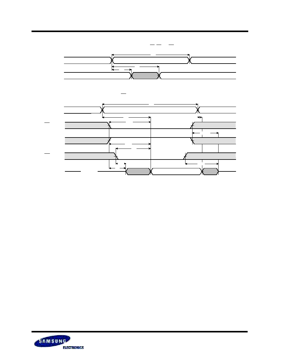
TIMMING DIAGRAMS
TIMING WAVEFORM OF READ CYCLE(1)
(Address Controlled
,
CS=OE=V
IL
, WE=V
IH
)
t
AA
t
RC
t
OH
TIMING WAVEFORM OF READ CYCLE(2)
(WE=V
IH
)
Data Valid
High-Z
CS
1
Address
OE
Data out
NOTES (READ CYCLE)
1.
t
HZ
and
t
OHZ
are defined as the time at which the outputs achieve the open circuit conditions and are not referenced to output voltage
levels.
2. At any given temperature and voltage condition,
t
HZ
(Max.) is less than
t
LZ
(Min.) both for a given device and from device to device
interconnection.
CS
2
t
OH
t
AA
t
OLZ
t
LZ
t
OHZ
t
HZ(1,2)
t
RC
t
CO2
t
OE
t
CO1
K6T1008V2C, K6T1008U2C Family
CMOS SRAM
Revision 2.0
November 1997
7
TIMING WAVEFORM OF WRITE CYCLE(1)
(WE Controlled)
Address
CS
1
t
CW(2)
t
WR(4)
TIMING WAVEFORM OF WRITE CYCLE(2)
(CS
1
Controlled)
Address
CS
1
t
WC
t
WR(4)
t
AS(3)
CS
2
t
CW(2)
t
WP(1)
t
DW
t
DH
t
OW
t
WHZ
Data Undefined
Data Valid
WE
Data in
Data out
t
DW
t
DH
Data Valid
WE
Data in
Data out
High-Z
High-Z
CS
2
t
WC
t
AW
t
AS(3)
t
CW(2)
t
WP(1)
t
AW

K6T1008V2C, K6T1008U2C Family
CMOS SRAM
Revision 2.0
November 1997
8
DATA RETENTION WAVE FORM
CS
1
controlled
V
CC
3.0/2.7V
1)
2.2V
V
DR
CS
1
GND
Data Retention Mode
CS
1
V
CC
-0.2V
t
SDR
t
RDR
TIMING WAVEFORM OF WRITE CYCLE(3)
(CS
2
Controlled)
Address
CS
1
t
AW
NOTES (WRITE CYCLE)
1. A write occurs during the overlap of a low CS
1
, a high CS
2
and a low WE. A write begins at the latest transition among CS
1
goes low,
CS
2
going high and WE going low: A write end at the earliest transition among CS
1
going high, CS
2
going low and WE going high,
t
WP
is measured from the beginning of write to the end of write.
2. t
CW
is measured from the CS
1
going low or CS
2
going high to the end of write.
3. t
AS
is measured from the address valid to the beginning of write.
4. t
WR
is measured from the end of write to the address change. t
WR(1)
applied in case a write ends as CS
1
or WE going high t
WR(2)
applied in case a write ends as CS
2
going to low.
CS
2
t
CW(2)
WE
Data in
Data Valid
Data out
High-Z
High-Z
t
CW(2)
t
WR(4)
t
WP(1)
t
DW
t
DH
t
AS(3)
t
WC
CS
2
controlled
V
CC
3.0/2.7V
1)
0.4V
V
DR
CS
2
GND
Data Retention Mode
t
SDR
t
RDR
1. 3.0V for K6T1008V2C Family, 2.7V for K6T1008U2C Family
CS
2
0.2V
K6T1008V2C, K6T1008U2C Family
CMOS SRAM
Revision 2.0
November 1997
9
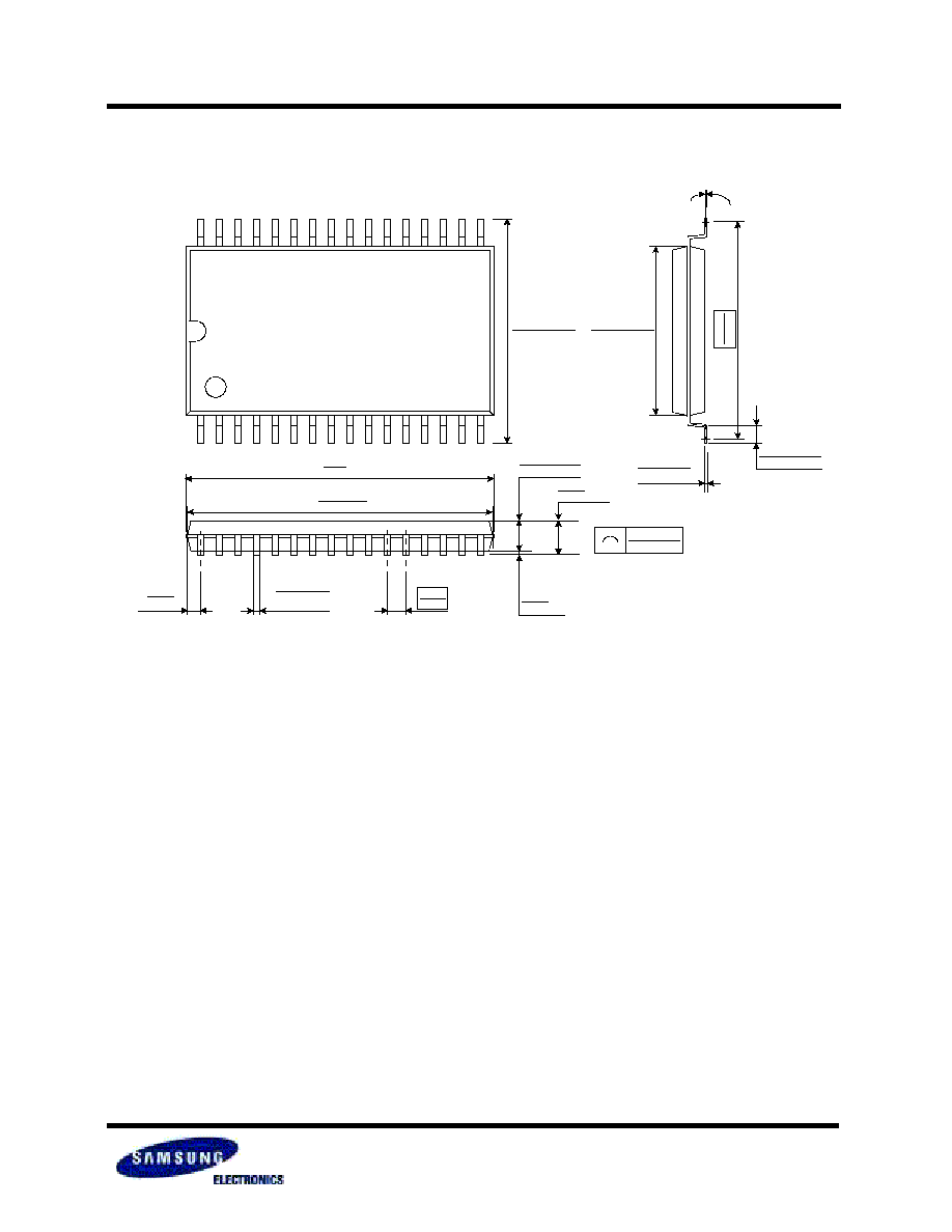
PACKAGE DIMENSIONS
Units: millimeter(inch)
32 PIN PLASTIC SMALL OUTLINE PACKAGE (525mil)
0~8
∞
#32
20.47
±
0.20
0.806
±
0.008
MAX
20.87
0.822
MAX
2.74
±
0.20
0.108
±
0.008
3.00
0.118
MIN
0.002
0.05
0.004 MAX
0.10 MAX
#1
0.71
( )
0.028
1
3
.
3
4
0
.
5
2
5
11.43
±
0.20
0.450
±
0.008
0.80
±
0.20
0.031
±
0.008
+0.10
0.20
-0.05
+0.004
0.008
-0.002
14.12
±
0.30
0.556
±
0.012
#17
#16
1.27
0.050
+0.100
0.41
-0.050
+0.004
0.016
-0.002
K6T1008V2C, K6T1008U2C Family
CMOS SRAM
Revision 2.0
November 1997
10
#32
1.00
±
0.10
0.039
±
0.004
M
A
X
8
.
4
0
0
.
3
3
1
0
.
0
0
4
0
.
1
0
#1
13.40
±
0.20
0.528
±
0.008
#17
#16
+0.10
0.20
-0.05
+0.004
0.008
-0.002
0.50
0.0197
0.25
( )
0.010
MIN
0.05
0.002
MAX
1.20
0.047
8
.
0
0
0
.
3
1
5
M
A
X
#32
1.00
±
0.10
0.039
±
0.004
M
A
X
8
.
4
0
0
.
3
3
1
#1
0.50
( )
0.020
11.80
±
0.10
0.465
±
0.004
0.45~0.75
0.018~0.030
13.40
±
0.20
0.528
±
0.008
#17
#16
+0.10
0.15
-0.05
+0.004
0.006
-0.002
0~8
∞
+0.10
0.20
-0.05
+0.004
0.008
-0.002
0.50
0.0197
0.25
( )
0.010
MIN
0.05
0.002
MAX
1.20
0.047
8
.
0
0
0
.
3
1
5
TYP
0.25
0.010
0
.
0
0
4
0
.
1
0
M
A
X
0.50
( )
0.020
11.80
±
0.10
0.465
±
0.004
0.45~0.75
0.018~0.030
+0.10
0.15
-0.05
+0.004
0.006
-0.002
0~8
∞
TYP
0.25
0.010
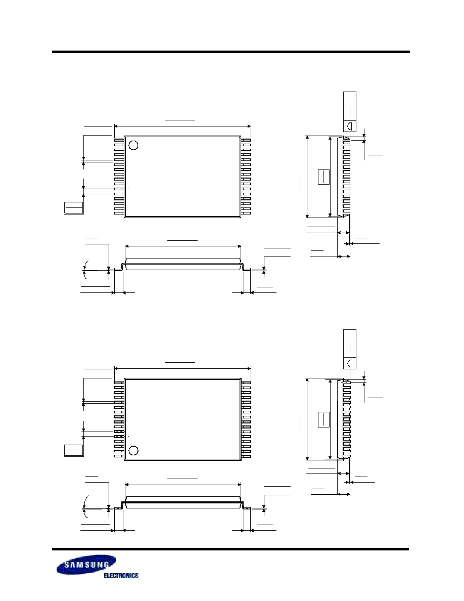
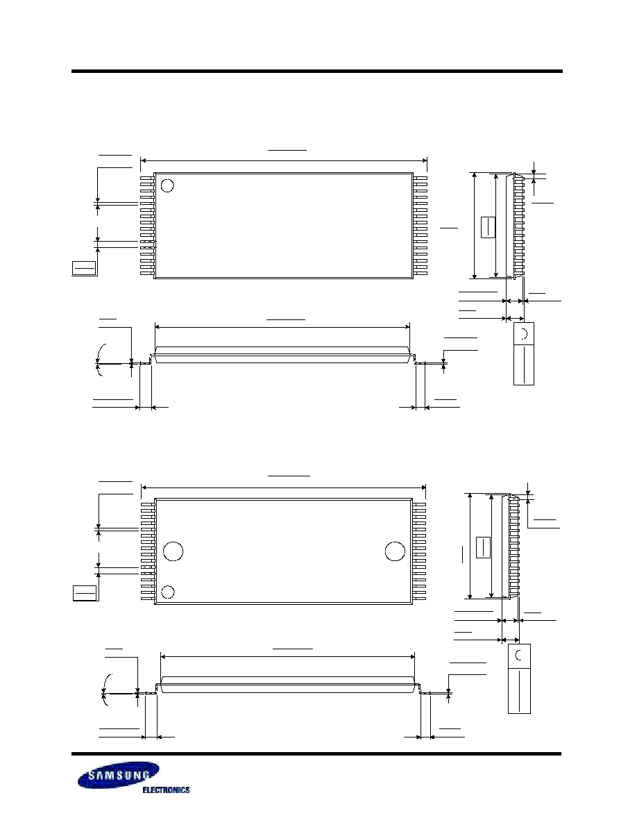
32 PIN THIN SMALL OUTLINE PACKAGE TYPE I (0813.4F)
PACKAGE DIMENSIONS
32 PIN THIN SMALL OUTLINE PACKAGE TYPE I (0813.4R)
Units: millimeter(inch)
K6T1008V2C, K6T1008U2C Family
CMOS SRAM
Revision 2.0
November 1997
11
32 PIN THIN SMALL OUTLINE PACKAGE TYPE I (0820F)
#32
1.00
±
0.10
0.039
±
0.004
MAX
8.40
0.331
0
.
1
0
M
A
X
0
.
0
0
4
M
A
X
#1
0.50
( )
0.020
18.40
±
0.10
0.724
±
0.004
0.45 ~0.75
0.018 ~0.030
20.00
±
0.20
0.787
±
0.008
#17
+0.10
0.15
-0.05
+0.004
0.006
-0.002
0~8
∞
+0.10
0.20
-0.05
+0.004
0.008
-0.002
0.50
0.0197
0.25
( )
0.010
MIN
0.05
0.002
MAX
1.20
0.047
8
.
0
0
0
.
3
1
5
TYP
0.25
0.010
#16
PACKAGE DIMENSIONS
32 PIN THIN SMALL OUTLINE PACKAGE TYPE I (0820R)
#32
1.00
±
0.10
0.039
±
0.004
M
A
X
8
.
4
0
0
.
3
3
1
0
.
0
0
4
M
A
X
0
.
1
0
M
A
X
#1
0.50
( )
0.020
18.40
±
0.10
0.724
±
0.004
0.45 ~0.75
0.018 ~0.030
20.00
±
0.20
0.787
±
0.008
#17
+0.10
0.15
-0.05
+0.004
0.006
-0.002
0~8
∞
+0.10
0.20
-0.05
+0.004
0.008
-0.002
0.50
0.0197
0.25
( )
0.010
MIN
0.05
0.002
MAX
1.20
0.047
8
.
0
0
0
.
3
1
5
TYP
0.25
0.010
#16
Units: millimeter(inch)