K6T4008V1C, K6T4008U1C Family
CMOS SRAM
Revision 1.0
January 1999
2
512K
◊
8 bit Low Power and Low Voltage CMOS Static RAM
GENERAL DESCRIPTION
The K6T4008V1C and K6T4008U1C families are fabricated by
SAMSUNG
s advanced CMOS process technology. The fami-
lies support various operating temperature range and have var-
ious package type for user flexibility of system design. The
families also support low data retention voltage for battery
back-up operation with low data retention current.
FEATURES
∑
Process Technology: TFT
∑
Organization: 512K
◊
8
∑
Power Supply Voltage
K6T4008V1C Family: 3.0~3.6V
K6T4008U1C Family: 2.7~3.3V
∑
Low Data Retention Voltage: 2V(Min)
∑
Three state output and TTL Compatible
∑
Package Type: 32-SOP-525, 32-TSOP2-400F/R
32-TSOP1-0820F, 32-TSOP1-0813.4F
PIN DESCRIPTION
Name
Function
Name
Function
A
0
~A
18
Address Inputs
Vcc
Power
WE
Write Enable Input
Vss
Ground
CS
Chip Select Input
I/O
1
~I/O
8
Data Inputs/Outputs
OE
Output Enable Input
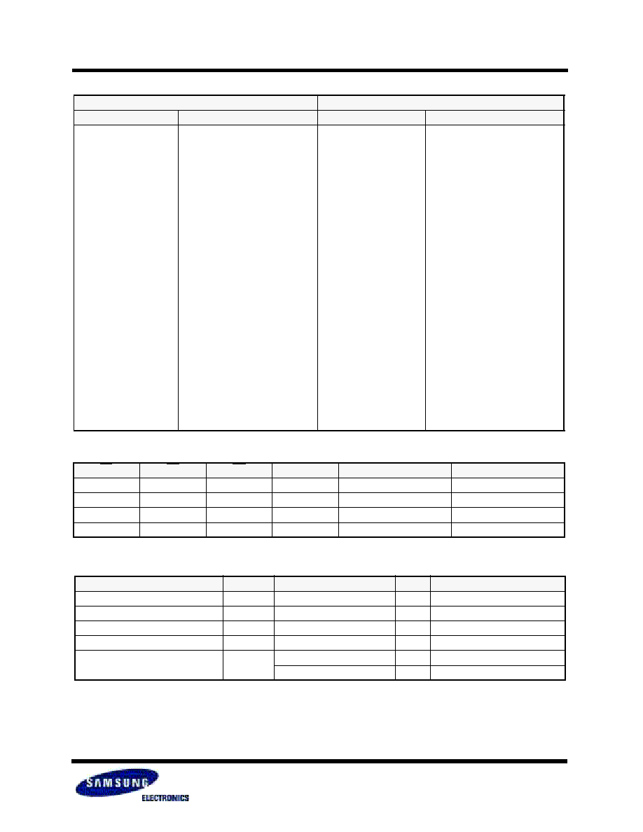
PRODUCT FAMILY
1. The paramerter is measured with 30pF test load.
Product Family
Operating Temperature
Vcc Range
Speed
Power Dissipation
PKG Type
Standby
(I
SB1
, Max)
Operating
(I
CC2
, Max)
K6T4008V1C-B
Commercial(0~70
∞
C)
3.0~3.6V
70
1)
/85ns
15
µ
A
30mA
32-SOP
32-TSOP2-F/R
32-TSOP1-F
32-sTSOP1-F
K6T4008U1C-B
2.7~3.3V
70
1)
/85/100ns
K6T4008V1C-F
Industrial(-40~85
∞
C)
3.0~3.6V
70
1)
/85ns
20
µ
A
K6T4008U1C-F
2.7~3.3V
70
1)
/85/100ns
FUNCTIONAL BLOCK DIAGRAM
32-SOP
(Forward)
32-TSOP2
A16
A14
A12
A7
A6
A5
A4
A3
A2
A1
A0
I/O1
I/O2
I/O3
VSS
VCC
A15
WE
A13
A8
A9
A11
OE
A10
CS
I/O8
I/O7
I/O6
I/O5
I/O4
32
31
30
29
28
27
26
25
24
23
22
21
20
19
18
17
1
2
3
4
5
6
7
8
9
10
11
12
13
14
15
16
32-TSOP2
A16
A14
A12
A7
A6
A5
A4
A3
A2
A1
A0
I/O1
I/O2
I/O3
VSS
VCC
A15
WE
A13
A8
A9
A11
OE
A10
CS
I/O8
I/O7
I/O6
I/O5
I/O4
32
31
30
29
28
27
26
25
24
23
22
21
20
19
18
17
1
2
3
4
5
6
7
8
9
10
11
12
13
14
15
16
(Reverse)
A18
A17
A17
A18
SAMSUNG ELECTRONICS CO., LTD. reserves the right to change products and specifications without notice.
A15
Precharge circuit.
Memory array
1024 rows
512
◊
8 columns
I/O Circuit
Column select
Clk gen.
Row
select
A2 A3 A8 A9 A10
A13
A11
A0
A1
A4
A5
A6
A7
A14
CS
WE
I/O
1
Data
cont
Data
cont
OE
I/O
8
A12
A16
A18
A11
A9
A8
A13
WE
A17
A15
VCC
A18
A16
A14
A12
A7
A6
A5
A4
OE
A10
CS
I/O8
I/O7
I/O6
I/O5
I/O4
VSS
I/O3
I/O2
I/O1
A0
A1
A2
A3
32-TSOP1
(Forward)
32
31
30
29
28
27
26
25
24
23
22
21
20
19
18
17
1
2
3
4
5
6
7
8
9
10
11
12
13
14
15
16
A17
Control
logic
32-
S
TSOP1
K6T4008V1C, K6T4008U1C Family
CMOS SRAM
Revision 1.0
January 1999
3
PRODUCT LIST
Commercial Temp Products(0~70
∞
C)
Industrial Temp Products(-40~85
∞
C)
Part Name
Function
Part Name
Function
K6T4008V1C-GB70
K6T4008V1C-GB85
K6T4008V1C-VB70
K6T4008V1C-VB85
K6T4008V1C-MB70
K6T4008V1C-MB85
K6T4008V1C-TB70
K6T4008V1C-TB85
K6T4008V1C-YB70
K6T4008V1C-YB85
K6T4008U1C-GB70
K6T4008U1C-GB85
K6T4008U1C-GB10
K6T4008U1C-VB70
K6T4008U1C-VB85
K6T4008U1C-VB10
K6T4008U1C-MB70
K6T4008U1C-MB85
K6T4008U1C-MB10
K6T4008U1C-TB70
K6T4008U1C-TB85
K6T4008U1C-TB10
K6T4008U1C-YB70
K6T4008U1C-YB85
K6T4008U1C-YB10
32-SOP, 70ns, 3.3V, LL
32-SOP, 85ns, 3.3V, LL
32-TSOP2-F, 70ns, 3.3V, LL
32-TSOP2-F, 85ns, 3.3V, LL
32-TSOP2-R, 70ns, 3.3V, LL
32-TSOP2-R, 85ns, 3.3V, LL
32-TSOP1-F, 70ns, 3.3V, LL
32-TSOP1-F, 85ns, 3.3V, LL
32-sTSOP1-F, 70ns, 3.3V, LL
32-sTSOP1-F, 85ns, 3.3V, LL
32-SOP, 70ns, 3.0V, LL
32-SOP, 85ns, 3.0V, LL
32-SOP, 100ns, 3.0V, LL
32-TSOP2-F, 70ns, 3.0V, LL
32-TSOP2-F, 85ns, 3.0V, LL
32-TSOP2-F, 100ns, 3.0V, LL
32-TSOP2-R, 70ns, 3.0V, LL
32-TSOP2-R, 85ns, 3.0V, LL
32-TSOP2-R, 100ns, 3.0V, LL
32-TSOP1-F, 70ns, 3.0V, LL
32-TSOP1-F, 85ns, 3.0V, LL
32-TSOP1-F, 100ns, 3.0V, LL
32-sTSOP1-F, 70ns, 3.0V, LL
32-sTSOP1-F, 85ns, 3.0V, LL
32-sTSOP1-F, 100ns, 3.0V, LL
K6T4008V1C-GF70
K6T4008V1C-GF85
K6T4008V1C-VF70
K6T4008V1C-VF85
K6T4008V1C-MF70
K6T4008V1C-MF85
K6T4008V1C-TF70
K6T4008V1C-TF85
K6T4008V1C-YF70
K6T4008V1C-YF85
K6T4008U1C-GF70
K6T4008U1C-GF85
K6T4008U1C-GF10
K6T4008U1C-VF70
K6T4008U1C-VF85
K6T4008U1C-VF10
K6T4008U1C-MF70
K6T4008U1C-MF85
K6T4008U1C-MF10
K6T4008U1C-TF70
K6T4008U1C-TF85
K6T4008U1C-TF10
K6T4008U1C-YF70
K6T4008U1C-YF85
K6T4008U1C-YF10
32-SOP, 70ns, 3.3V, LL
32-SOP, 85ns, 3.3V, LL
32-TSOP2-F, 70ns, 3.3V, LL
32-TSOP2-F, 85ns, 3.3V, LL
32-TSOP2-R, 70ns, 3.3V, LL
32-TSOP2-R, 85ns, 3.3V, LL
32-TSOP1-F, 70ns, 3.3V, LL
32-TSOP1-F, 85ns, 3.3V, LL
32-sTSOP1-F, 70ns, 3.3V, LL
32-sTSOP1-F, 85ns, 3.3V, LL
32-SOP, 70ns, 3.0V, LL
32-SOP, 85ns, 3.0V, LL
32-SOP, 100ns, 3.0V, LL
32-TSOP2-F, 70ns, 3.0V, LL
32-TSOP2-F, 85ns, 3.0V, LL
32-TSOP2-F, 100ns, 3.0V, LL
32-TSOP2-R, 70ns, 3.0V, LL
32-TSOP2-R, 85ns, 3.0V, LL
32-TSOP2-R, 100ns, 3.0V, LL
32-TSOP1-F, 70ns, 3.0V, LL
32-TSOP1-F, 85ns, 3.0V, LL
32-TSOP1-F, 100ns, 3.0V, LL
32-sTSOP1-F, 70ns, 3.0V, LL
32-sTSOP1-F, 85ns, 3.0V, LL
32-sTSOP1-F, 100ns, 3.0V, LL
FUNCTIONAL DESCRIPTION
1. X means don
t care (Must be in low or high state)
CS
OE
WE
I/O
Mode
Power
H
X
1)
X
1)
High-Z
Deselected
Standby
L
H
H
High-Z
Output Disabled
Active
L
L
H
Dout
Read
Active
L
X
1)
L
Din
Write
Active
ABSOLUTE MAXIMUM RATINGS
1)
1. Stresses greater than those listed under "Absolute Maximum Ratings" may cause permanent damage to the device. Functional operation should be
restricted to recommended operating condition. Exposure to absolute maximum rating conditions for extended periods may affect reliability.
Item
Symbol
Ratings
Unit
Remark
Voltage on any pin relative to Vss
V
IN
,V
OUT
-0.5 to V
CC
+0.5
V
-
Voltage on Vcc supply relative to Vss
V
CC
-0.3 to 4.6
V
-
Power Dissipation
P
D
1.0
W
-
Storage temperature
T
STG
-65 to 150
∞
C
-
Operating Temperature
T
A
0 to 70
∞
C
K6T4008V1C-L, K6T4008U1C-L
-40 to 85
∞
C
K6T4008V1C-P, K6T4008U1C-P
K6T4008V1C, K6T4008U1C Family
CMOS SRAM
Revision 1.0
January 1999
4
RECOMMENDED DC OPERATING CONDITIONS
1)
Note:
1. Commercial Product : T
A
=0 to 70
∞
C, otherwise specified
Industrial Product : T
A
=-40 to 85
∞
C, otherwise specified
2. Overshoot : V
CC
+2.0V in case of pulse width
30ns
3. Undershoot : -2.0V in case of pulse width
30ns
4. Overshoot and undershoot are sampled, not 100% tested.
Item
Symbol
Product
Min
Typ
Max
Unit
Supply voltage
Vcc
K6T4008V1C Family
K6T4008U1C Family
3.0
2.7
3.3
3.0
3.6
3.3
V
Ground
Vss
All Family
0
0
0
V
Input high voltage
V
IH
K6T4008V1C, K6T4008U1C Family
2.2
-
Vcc+0.3
2)
V
Input low voltage
V
IL
K6T4008V1C, K6T4008U1C Family
-0.3
3)
-
0.6
V
CAPACITANCE
1)
(f=1MHz, T
A
=25
∞
C)
1. Capacitance is sampled, not 100% tested
Item
Symbol
Test Condition
Min
Max
Unit
Input capacitance
C
IN
V
IN
=0V
-
8
pF
Input/Output capacitance
C
IO
V
IO
=0V
-
10
pF
DC AND OPERATING CHARACTERISTICS
1. Industrial product = 20
µ
A
Item
Symbol
Test Conditions
Min
Typ
Max
Unit
Input leakage current
I
LI
V
IN
=Vss to Vcc
-1
-
1
µ
A
Output leakage current
I
LO
CS=V
IH
or OE=V
IH
or WE=V
IL
V
IO
=Vss to Vcc
-1
-
1
µ
A
Operating power supply current
I
CC
I
IO
=0mA, CS=V
IL
, V
IN
=V
IL
or V
IH
, Read
-
-
4
mA
Average operating current
I
CC1
Cycle time=1
µ
s, 100% duty, I
IO
=0mA CS
0.2V,V
IN
0.2V or V
IN
Vcc-0.2V
-
-
4
mA
I
CC2
Cycle time=Min, 100% duty, I
IO
=0mA, CS=V
IL,
V
IN
=V
IH
or V
IL
-
-
30
mA
Output low voltage
V
OL
I
OL
=2.1mA
-
-
0.4
V
Output high voltage
V
OH
I
OH
=-1.0mA
2.2
-
-
V
Standby Current(TTL)
I
SB
CS=V
IH
, Other inputs = V
IL
or V
IH
-
-
0.3
mA
Standby Current (CMOS)
I
SB1
CS
Vcc-0.2V, Other inputs=0~Vcc
-
-
15
1)
µ
A
K6T4008V1C, K6T4008U1C Family
CMOS SRAM
Revision 1.0
January 1999
5
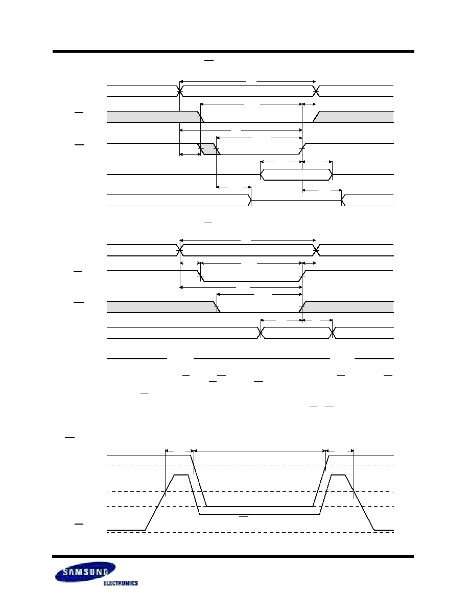
AC CHARACTERISTICS
(K6T4008V1C Family: Vcc=3.0~3.6V, K6T4008U1C Family: Vcc=2.7~3.3V
Commercial product:: T
A
=0 to 70
∞
C, Industrial product: T
A
=-40 to 85
∞
C)
Parameter List
Symbol
Speed Bins
Units
70ns
85ns
100ns
Min
Max
Min
Max
Min
Max
Read
Read cycle time
t
RC
70
-
85
-
100
-
ns
Address access time
t
AA
-
70
-
85
-
100
ns
Chip select to output
t
CO
-
70
-
85
-
100
ns
Output enable to valid output
t
OE
-
35
-
40
-
50
ns
Chip select to low-Z output
t
LZ
10
-
10
-
10
-
ns
Output enable to low-Z output
t
OLZ
5
-
5
-
5
-
ns
Chip disable to high-Z output
t
HZ
0
25
0
25
0
30
ns
Output disable to high-Z output
t
OHZ
0
25
0
25
0
30
ns
Output hold from address change
t
OH
10
-
10
-
15
-
ns
Write
Write cycle time
t
WC
70
-
85
-
100
-
ns
Chip select to end of write
t
CW
60
-
70
-
80
-
ns
Address set-up time
t
AS
0
-
0
-
0
-
ns
Address valid to end of write
t
AW
60
-
70
-
80
-
ns
Write pulse width
t
WP
55
-
55
-
70
-
ns
Write recovery time
t
WR
0
-
0
-
0
-
ns
Write to output high-Z
t
WHZ
0
25
0
25
0
30
ns
Data to write time overlap
t
DW
30
-
35
-
40
-
ns
Data hold from write time
t
DH
0
-
0
-
0
-
ns
End write to output low-Z
t
OW
5
-
5
-
5
-
ns
C
L
1)
1. Including scope and jig capacitance
AC OPERATING CONDITIONS
TEST CONDITIONS
(Test Load and Input/Output Reference)
Input pulse level: 0.4 to 2.2V
Input rising and falling time: 5ns
Input and output reference voltage:1.5V
Output load(see right): C
L
=100pF+1TTL
C
L
1)
=30pF+1TTL
1. 70ns product
DATA RETENTION CHARACTERISTICS
1. Industrial product = 20
µ
A
Item
Symbol
Test Condition
Min
Typ
Max
Unit
Vcc for data retention
V
DR
CS
Vcc-0.2V
2.0
-
3.6
V
Data retention current
I
DR
Vcc=3.0V, CS
Vcc-0.2V
-
0.5
15
1)
µ
A
Data retention set-up time
t
SDR
See data retention waveform
0
-
-
ms
Recovery time
t
RDR
5
-
-