þÿ
512Kx36 & 1Mx18 Synchronous SRAM
- 1 -
Rev 3.0
Nov. 2003
K7A161800A
K7A163600A
Document Title
512Kx36/x32 & 1Mx18-Bit Synchronous Pipelined Burst SRAM
Revision History
Rev. No.
0.0
0.1
0.2
0.3
1.0
2.0
2.1
3.0
Remark
Preliminary
Preliminary
Preliminary
Preliminary
Final
Final
Final
Final
History
Initial draft
1. Add JTAG Scan Order
1. Add x32 org and industrial temperature .
2. Add 165FBGA package
1. Speed Bin Merge
From K7A1636(32/18)09A to K7A1636(32/18)00A
2. AC parameter change
tOH(min)/tHZC(min) from 0.8 to 1.5 at -25
tOH(min)/tHZC(min) from 1.0 to 1.5 at -22
tOH(min)/tHZC(min) from 1.0 to 1.5 at -20
1. Final spec release
1. Release Icc.
1. Delete 119BGA package.
2. Correct the Ball Size of 165 FBGA.
1. Delete x32 Org.
2. Delete 165FBGA package.
3. Delelte the 225MHz and 200MHz speed bin.
part #
From
To
-25
440
470
-22
400
430
-20
370
400
-16
340
350
-14
280
290
Draft Date
Feb. 23. 2001
May. 10. 2001
Aug. 31. 2001
Dec. 26. 2001
May. 10. 2002
May. 22. 2002
April 04. 2003
Nov. 17, 2003
512Kx36 & 1Mx18 Synchronous SRAM
- 2 -
Rev 3.0
Nov. 2003
K7A161800A
K7A163600A
16Mb SB/SPB Synchronous SRAM Ordering Information
Org.
Part Number
Mode
VDD
Speed
SB ; Access Time(ns)
SPB ; Cycle Time(MHz)
PKG
Temp
1Mx18
K7B161825A-QC(I)75/85
SB
3.3
7.5/8.5ns
Q : 100TQFP
C
; Commercial
Temp.Range
I
; Industrial
Temp.Range
K7A161800A-QC(I)25/16/14
SPB(2E1D)
3.3
250/167/138MHz
K7A161801A-QC(I)20/16
SPB(2E2D)
3.3
200/167MHz
512Kx36
K7B163625A-QC(I)75/85
SB
3.3
7.5/8.5ns
K7A163600A-QC(I)25/16/14
SPB(2E1D)
3.3
250/167/138MHz
K7A163601A-QC(I)20/16
SPB(2E2D)
3.3
200/167MHz
512Kx36 & 1Mx18 Synchronous SRAM
- 3 -
Rev 3.0
Nov. 2003
K7A161800A
K7A163600A
512Kx36 & 1Mx18-Bit Synchronous Pipelined Burst SRAM
The K7A163600A and K7A161800A are 18,874,368-bit
Synchronous Static Random Access Memory designed for
high performance second level cache of Pentium and
Power PC based System.
It is organized as 512K(1M) words of 36(32/18) bits and
integrates address and control registers, a 2-bit burst
address counter and added some new functions for high
performance cache RAM applications; GW, BW, LBO , ZZ.
Write cycles are internally self-timed and synchronous.
Full bus-width write is done by G W, and each byte write is
performed by the combination of WEx and BW when GW is
high. And with CS
1
high, ADSP is blocked to control sig-
nals.
Burst cycle can be initiated with either the address status
processor (ADSP) or address status cache controller
(ADSC) inputs. Subsequent burst addresses are generated
internally in the system
s burst sequence and are con-
trolled by the burst address advance(ADV ) input.
LBO pin is DC operated and determines burst sequence
(linear or interleaved).
ZZ pin controls Power Down State and reduces Stand-by
current regardless of CLK.
The K7A163600A and K7A161800A are fabricated using
SAMSUNG
s high performance CMOS technology and is
available in a 100pin TQFP. Multiple power and ground
pins are utilized to minimize ground bounce.
GENERAL DESCRIPTION
FEATURES
LOGIC BLOCK DIAGRAM
·
Synchronous Operation.
·
2 Stage Pipelined operation with 4 Burst.
·
On-Chip Address Counter.
·
Self-Timed Write Cycle.
·
On-Chip Address and Control Registers.
·
V
DD
= 3.3V +0.165V/-0.165V Power Supply.
· I/O Supply Voltage 3.3V +0.165V/-0.165V for 3.3V I/O
or 2.5V+0.4V/-0.125V for 2.5V I/O.
·
5V Tolerant Inputs Except I/O Pins.
·
Byte Writable Function.
·
Global Write Enable Controls a full bus-width write.
·
Power Down State via ZZ Signal.
·
LBO Pin allows a choice of either a interleaved burst or a linear
burst.
·
Three Chip Enables for simple depth expansion with No Data Con-
tention only for TQFP ; 2cycle Enable, 1cycle Disable.
·
Asynchronous Output Enable Control.
·
ADSP, ADSC, ADV Burst Control Pins.
·
TTL-Level Three-State Output.
·
100-TQFP-1420A
· Operating in commeical and industrial temperature range.
CLK
LBO
ADV
ADSC
ADSP
CS
1
CS
2
CS
2
GW
BW
WEx
OE
ZZ
DQa
0
~ DQd
7
or DQa0 ~ DQb7
BURST CONTROL
LOGIC
BURST
512Kx36, 1Mx18
ADDRESS
CONTROL
OUTPUT
DATA-IN
ADDRESS
COUNTER
MEMORY
ARRAY
REGISTER
REGISTER
BUFFER
LOGIC
C
O
N
T
R
O
L
R
E
G
I
S
T
E
R
C
O
N
T
R
O
L
R
E
G
I
S
T
E
R
A
0
~A
1
A
0
~A
1
or A
2
~A
19
or A
0
~A
19
REGISTER
DQPa ~ DQPd
A
0
~A
18
A
2
~A
18
(x=a,b,c,d or a,b)
DQPa,DQPb
FAST ACCESS TIMES
PARAMETER
Symbol
-25
-16
-14
Unit
Cycle Time
t
CYC
4.0
6.0
7.2
ns
Clock Access Time
t
CD
2.6
3.5
4.0
ns
Output Enable Access Time
t
OE
2.6
3.5
4.0
ns
512Kx36 & 1Mx18 Synchronous SRAM
- 4 -
Rev 3.0
Nov. 2003
K7A161800A
K7A163600A
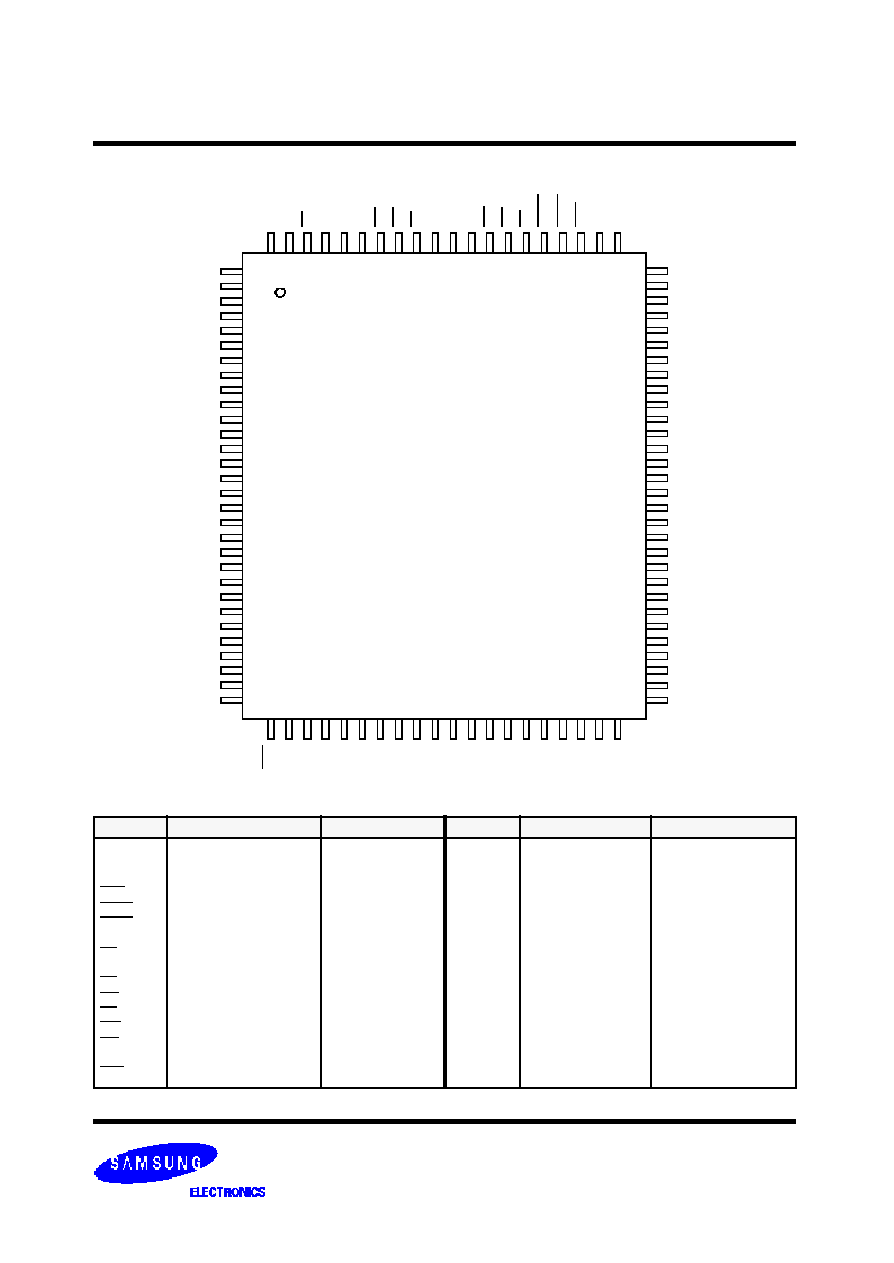
PIN CONFIGURATION
(TOP VIEW)
PIN NAME
Note :
1. A0 and A1 are the two least significant bits(LSB) of the address field and set the internal burst counter if burst is desired.
SYMBOL
PIN NAME
TQFP PIN NO.
SYMBOL
PIN NAME
TQFP PIN NO.
A
0
- A
18
ADV
ADSP
ADSC
CLK
CS
1
CS
2
CS
2
WE x(x=a,b,c,d)
OE
GW
BW
ZZ
LBO
Address Inputs
Burst Address Advance
Address Status Processor
Address Status Controller
Clock
Chip Select
Chip Select
Chip Select
Byte Write Inputs
Output Enable
Global Write Enable
Byte Write Enable
Power Down Input
Burst Mode Control
32,33,34,35,36,37,42
43,44,45,46,47,48,49
50,81,82,99,100
83
84
85
89
98
97
92
93,94,95,96
86
88
87
64
31
V
DD
V
SS
N.C.
DQa
0
~a
7
DQb
0
~b
7
DQc
0
~c
7
DQd
0
~d
7
DQPa~P
d
or N.C
V
DDQ
V
SSQ
Power Supply(+3.3V)
Ground
No Connect
Data Inputs/Outputs
Output Power Supply
(3.3V or 2.5V)
Output Ground
15,41,65,91
17,40,67,90
14,16,38,39,66
52,53,56,57,58,59,62,63
68,69,72,73,74,75,78,79
2,3,6,7,8,9,12,13
18,19,22,23,24,25,28,29
51,80,1,30
4,11,20,27,54,61,70,77
5,10,21,26,55,60,71,76
1
2
3
4
5
6
7
8
9
10
11
12
13
14
15
16
17
18
19
20
21
22
23
24
25
26
27
28
29
30
100 Pin TQFP
(20mm x 14mm)
NC/DQPc
DQc
0
DQc
1
V
DDQ
V
SSQ
DQc
2
DQc
3
DQc
4
DQc
5
V
SSQ
V
DDQ
DQc
6
DQc
7
N.C.
V
DD
N.C.
V
SS
DQd
0
DQd
1
V
DDQ
V
SSQ
DQd
2
DQd
3
DQd
4
DQd
5
V
SSQ
V
DDQ
DQd
6
DQd
7
NC/DQPd
80
79
78
77
76
75
74
73
72
71
70
69
68
67
66
65
64
63
62
61
60
59
58
57
56
55
54
53
52
51
DQPb/NC
DQb
7
DQb
6
V
DDQ
V
SSQ
DQb
5
DQb
4
DQb
3
DQb
2
V
SSQ
V
DDQ
DQb
1
DQb
0
V
SS
N.C.
V
DD
ZZ
DQa
7
DQa
6
V
DDQ
V
SSQ
DQa
5
DQa
4
DQa
3
DQa
2
V
SSQ
V
DDQ
DQa
1
DQa
0
DQPa/NC
1
0
0
9
9
9
8
9
7
9
6
9
5
9
4
9
3
9
2
9
1
9
0
8
9
8
8
8
7
8
6
8
5
8
4
8
3
8
2
A
6
A
7
C
S
1
C
S
2
W
E
d
W
E
c
W
E
b
W
E
a
C
S
2
V
D
D
V
S
S
C
L
K
G
W
B
W
O
E
A
D
S
C
A
D
S
P
A
D
V
A
8
8
1
A
9
5
0
4
9
4
8
4
7
4
6
4
5
4
4
4
3
4
2
4
1
4
0
3
9
3
8
3
7
3
6
3
5
3
4
3
3
3
2
A
1
5
A
1
4
A
1
3
A
1
2
A
1
1
A
1
0
A
1
7
A
1
8
V
D
D
V
S
S
N
.
C
.
N
.
C
.
A
0
A
1
A
2
A
3
A
4
A
5
3
1
L
B
O
A
1
6
K7A163600A(512Kx36)
512Kx36 & 1Mx18 Synchronous SRAM
- 5 -
Rev 3.0
Nov. 2003
K7A161800A
K7A163600A
PIN CONFIGURATION
(TOP VIEW)
PIN NAME
Note :
1. A
0
and A
1
are the two least significant bits(LSB) of the address field and set the internal burst counter if burst is desired.
SYMBOL
PIN NAME
TQFP PIN NO.
SYMBOL
PIN NAME
TQFP PIN NO.
A
0
- A
19
ADV
ADSP
ADSC
CLK
CS
1
CS
2
CS
2
W Ex(x=a,b)
OE
G W
B W
ZZ
LBO
Address Inputs
Burst Address Advance
Address Status Processor
Address Status Controller
Clock
Chip Select
Chip Select
Chip Select
Byte Write Inputs
Output Enable
Global Write Enable
Byte Write Enable
Power Down Input
Burst Mode Control
32,33,34,35,36,37,42
43,44,45,46,47,48,49
50 80,81,82,99,100
83
84
85
89
98
97
92
93,94
86
88
87
64
31
V
DD
V
SS
N.C.
DQa
0
~ a
7
DQb
0
~ b
7
DQPa, Pb
V
DDQ
V
SSQ
Power Supply(+3.3V)
Ground
No Connect
Data Inputs/Outputs
Output Power Supply
(3.3V or 2.5V)
Output Ground
15,41,65,91
17,40,67,90
1,2,3,6,7,14,16,25,28,29
30,38,39,51,52,53,56,57
66,75,78,79,95,96
58,59,62,63,68,69,72,73
8,9,12,13,18,19,22,23
74,24
4,11,20,27,54,61,70,77
5,10,21,26,55,60,71,76
1
2
3
4
5
6
7
8
9
10
11
12
13
14
15
16
17
18
19
20
21
22
23
24
25
26
27
28
29
30
100 Pin TQFP
(20mm x 14mm)
N.C.
N.C.
N.C.
V
DDQ
V
SSQ
N.C.
N.C.
DQb
0
DQb
1
V
SSQ
V
DDQ
DQb
2
DQb
3
N.C.
V
DD
N.C.
V
SS
DQb
4
DQb
5
V
DDQ
V
SSQ
DQb
6
DQb
7
DQPb
N.C.
V
SSQ
V
DDQ
N.C.
N.C.
N.C.
80
79
78
77
76
75
74
73
72
71
70
69
68
67
66
65
64
63
62
61
60
59
58
57
56
55
54
53
52
51
N.C.
N.C.
V
DDQ
V
SSQ
N.C.
DQPa
DQa
7
DQa
6
V
SSQ
V
DDQ
DQa
5
DQa
4
V
SS
N.C.
V
DD
ZZ
DQa
3
DQa
2
V
DDQ
V
SSQ
DQa
1
DQa
0
N.C.
N.C.
V
SSQ
V
DDQ
N.C.
N.C.
N.C.
1
0
0
9
9
9
8
9
7
9
6
9
5
9
4
9
3
9
2
9
1
9
0
8
9
8
8
8
7
8
6
8
5
8
4
8
3
8
2
A
6
A
7
C
S
1
C
S
2
N
.
C
.
N
.
C
.
W
E
b
W
E
a
C
S
2
V
D
D
V
S
S
C
L
K
G
W
B
W
O
E
A
D
S
C
A
D
S
P
A
D
V
A
8
8
1
A
9
5
0
4
9
4
8
4
7
4
6
4
5
4
4
4
3
4
2
4
1
4
0
3
9
3
8
3
7
3
6
3
5
3
4
3
3
3
2
A
1
5
A
1
4
A
1
3
A
1
2
A
1
1
A
1
8
A
1
9
V
D
D
V
S
S
N
.
C
.
N
.
C
.
A
0
A
1
A
2
A
3
A
4
A
5
3
1
L
B
O
A
1
6
A
1
7
A
10
K7A161800A(1Mx18)
512Kx36 & 1Mx18 Synchronous SRAM
- 6 -
Rev 3.0
Nov. 2003
K7A161800A
K7A163600A
FUNCTION DESCRIPTION
The K7A163600A and K7A161800A are synchronous SRAM designed to support the burst address accessing sequence of the
Power PC based microprocessor. All inputs (with the exception of OE, LBO and ZZ) are sampled on rising clock edges. The start and
duration of the burst access is controlled by ADSC, ADSP and ADV and chip select pins.
The accesses are enabled with the chip select signals and output enabled signals. Wait states are inserted into the access with
ADV.
When ZZ is pulled high, the SRAM will enter a Power Down State. At this time, internal state of the SRAM is preserved. When ZZ
returns to low, the SRAM normally operates after 2cycles of wake up time. ZZ pin is pulled down internally.
Read cycles are initiated with ADSP(regardless of WEx and ADSC)using the new external address clocked into the on-chip address
register whenever ADSP is sampled low, the chip selects are sampled active, and the output buffer is enabled with OE. In read oper-
ation the data of cell array accessed by the current address, registered in the Data-out registers by the positive edge of CLK, are car-
ried to the Data-out buffer by the next positive edge of CLK. The data, registered in the Data-out buffer, are projected to the output
pins. ADV is ignored on the clock edge that samples ADSP asserted, but is sampled on the subsequent clock edges. The address
increases internally for the next access of the burst when W Ex are sampled High and ADV is sampled low. And ADSP is blocked to
control signals by disabling CS
1
.
All byte write is done by GW(regaedless of BW and W Ex.), and each byte write is performed by the combination of B W and WEx
when GW is high.
Write cycles are performed by disabling the output buffers with OE and asserting WEx. WEx are ignored on the clock edge that sam-
ples ADSP low, but are sampled on the subsequent clock edges. The output buffers are disabled when WEx are sampled
Low(regaedless of OE). Data is clocked into the data input register when WE x sampled Low. The address increases internally to the
next address of burst, if both WEx and ADV are sampled Low. Individual byte write cycles are performed by any one or more byte
write enable signals(WEa, WE b, WE c or WEd) sampled low. The W Ea control DQa
0
~ DQa
7
and DQPa, WE b controls DQb
0
~ DQb
7
and DQPb,
WEc controls DQc
0
~ DQc
7
and DQPc,
and WEd control DQd
0
~ DQd
7
and DQPd. Read or write cycle may also be initi-
ated with ADSC, instead of ADSP. The differences between cycles initiated with ADSC and ADSP as are follows;
ADSP must be sampled high when ADSC is sampled low to initiate a cycle with ADSC.
WEx are sampled on the same clock edge that sampled ADSC low(and ADSP high).
Addresses are generated for the burst access as shown below, The starting point of the burst sequence is provided by the external
address. The burst address counter wraps around to its initial state upon completion. The burst sequence is determined by the state
of the LBO pin. When this pin is Low, linear burst sequence is selected. When this pin is High, Interleaved burst sequence is
selected.
BURST SEQUENCE TABLE
(Interleaved Burst)
LBO PIN
HIGH
Case 1
Case 2
Case 3
Case 4
A
1
A
0
A
1
A
0
A
1
A
0
A
1
A
0
First Address
Fourth Address
0
0
1
1
0
1
0
1
0
0
1
1
1
0
1
0
1
1
0
0
0
1
0
1
1
1
0
0
1
0
1
0
BQ TABLE
(Linear Burst)
Note :
1. LBO pin must be tied to High or Low, and Floating State must not be allowed
.
LBO PIN
LOW
Case 1
Case 2
Case 3
Case 4
A
1
A
0
A
1
A
0
A
1
A
0
A
1
A
0
First Address
Fourth Address
0
0
1
1
0
1
0
1
0
1
1
0
1
0
1
0
1
1
0
0
0
1
0
1
1
0
0
1
1
0
1
0
ASYNCHRONOUS TRUTH TABLE
Operation
ZZ
O E
I/O STATUS
Sleep Mode
H
X
High-Z
Read
L
L
DQ
L
H
High-Z
Write
L
X
Din, High-Z
Deselected
L
X
High-Z
Notes
1. X means "Don
t Care".
2. ZZ pin is pulled down internally
3. For write cycles that following read cycles, the output buffers must be
disabled with OE, otherwise data bus contention will occur.
4. Sleep Mode means power down state of which stand-by current does
not depend on cycle time.
5. Deselected means power down state of which stand-by current
depends on cycle time.
512Kx36 & 1Mx18 Synchronous SRAM
- 7 -
Rev 3.0
Nov. 2003
K7A161800A
K7A163600A
SYNCHRONOUS TRUTH TABLE
Notes
: 1. X means "Don
t Care". 2. The rising edge of clock is symbolized by
.
3. WRITE = L means Write operation in WRITE TRUTH TABLE.
WRITE = H means Read operation in WRITE TRUTH TABLE.
4. Operation finally depends on status of asynchronous input pins(ZZ and OE).
CS
1
CS
2
CS
2
ADSP ADSC
ADV WRITE
CLK
ADDRESS ACCESSED
OPERATION
H
X
X
X
L
X
X
N/A
Not Selected
L
L
X
L
X
X
X
N/A
Not Selected
L
X
H
L
X
X
X
N/A
Not Selected
L
L
X
X
L
X
X
N/A
Not Selected
L
X
H
X
L
X
X
N/A
Not Selected
L
H
L
L
X
X
X
External Address
Begin Burst Read Cycle
L
H
L
H
L
X
L
External Address
Begin Burst Write Cycle
L
H
L
H
L
X
H
External Address
Begin Burst Read Cycle
X
X
X
H
H
L
H
Next Address
Continue Burst Read Cycle
H
X
X
X
H
L
H
Next Address
Continue Burst Read Cycle
X
X
X
H
H
L
L
Next Address
Continue Burst Write Cycle
H
X
X
X
H
L
L
Next Address
Continue Burst Write Cycle
X
X
X
H
H
H
H
Current Address
Suspend Burst Read Cycle
H
X
X
X
H
H
H
Current Address
Suspend Burst Read Cycle
X
X
X
H
H
H
L
Current Address
Suspend Burst Write Cycle
H
X
X
X
H
H
L
Current Address
Suspend Burst Write Cycle
TRUTH TABLES
WRITE TRUTH TABLE
(x36)
Notes
: 1. X means "Don
t Care".
2. All inputs in this table must meet setup and hold time around the rising edge of CLK(
) .
GW
BW
WEa
WEb
WEc
WE d
OPERATION
H
H
X
X
X
X
READ
H
L
H
H
H
H
READ
H
L
L
H
H
H
WRITE BYTE a
H
L
H
L
H
H
WRITE BYTE b
H
L
H
H
L
L
WRITE BYTE c and d
H
L
L
L
L
L
WRITE ALL BYTEs
L
X
X
X
X
X
WRITE ALL BYTEs
WRITE TRUTH TABLE
(x18)
Notes
: 1. X means "Don
t Care".
2. All inputs in this table must meet setup and hold time around the rising edge of CLK(
).
GW
BW
WEa
WEb
OPERATION
H
H
X
X
READ
H
L
H
H
READ
H
L
L
H
WRITE BYTE a
H
L
H
L
WRITE BYTE b
H
L
L
L
WRITE ALL BYTEs
L
X
X
X
WRITE ALL BYTEs
512Kx36 & 1Mx18 Synchronous SRAM
- 8 -
Rev 3.0
Nov. 2003
K7A161800A
K7A163600A
CAPACITANCE*
(T
A
=25
°
C, f=1MHz)
*Note
: Sampled not 100% tested.
PARAMETER
SYMBOL
TEST CONDITION
MIN
MAX
UNIT
Input Capacitance
C
IN
V
IN
=0V
-
5
pF
Output Capacitance
C
OUT
V
OUT
=0V
-
7
pF
OPERATING CONDITIONS at 3.3V I/O
(0
°
C
T
A
70
°
C)
* The above parameters are also guaranteed at industrial temperature range.
PARAMETER
SYMBOL
MIN
Typ.
MAX
UNIT
Supply Voltage
V
DD
3.135
3.3
3.465
V
V
DDQ
3.135
3.3
3.465
V
Ground
V
SS
0
0
0
V
OPERATING CONDITIONS at 2.5V I/O
(0
°
C
T
A
70
°
C)
* The above parameters are also guaranteed at industrial temperature range.
PARAMETER
SYMBOL
MIN
Typ.
MAX
UNIT
Supply Voltage
V
DD
3.135
3.3
3.465
V
V
DDQ
2.375
2.5
2.9
V
Ground
V
SS
0
0
0
V
ABSOLUTE MAXIMUM RATINGS*
*Note :
Stresses greater than those listed under "Absolute Maximum Ratings" may cause permanent damage to the device. This is a stress rating only
and functional operation of the device at these or any other conditions above those indicated in the operating sections of this specification is not
implied. Exposure to absolute maximum rating conditions for extended periods may affect reliability.
PARAMETER
SYMBOL
RATING
UNIT
Voltage on V
DD
Supply Relative to V
SS
V
DD
-0.3 to 4.6
V
Voltage on V
DDQ
Supply Relative to V
SS
V
DDQ
V
DD
V
Voltage on Input Pin Relative to V
SS
V
IN
-0.3 to V
DD
+0.3
V
Voltage on I/O Pin Relative to V
SS
V
IO
-0.3 to V
DDQ
+0.3
V
Power Dissipation
P
D
1.6
W
Storage Temperature
T
STG
-65 to 150
°
C
Operating Temperature
Commercial
T
OPR
0 to 70
°
C
Industrial
T
OPR
-40 to 85
°
C
Storage Temperature Range Under Bias
T
BIAS
-10 to 85
°
C
V
SS
V
IH
V
SS-
1.0V
20% t
CYC
(MIN)
512Kx36 & 1Mx18 Synchronous SRAM
- 9 -
Rev 3.0
Nov. 2003
K7A161800A
K7A163600A
V
SS
V
IH
V
SS-
1.0V
20% t
CYC
(MIN)
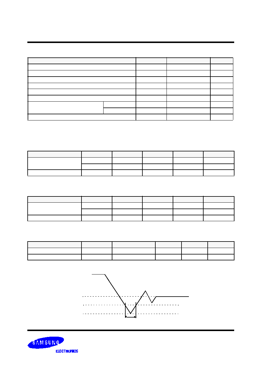
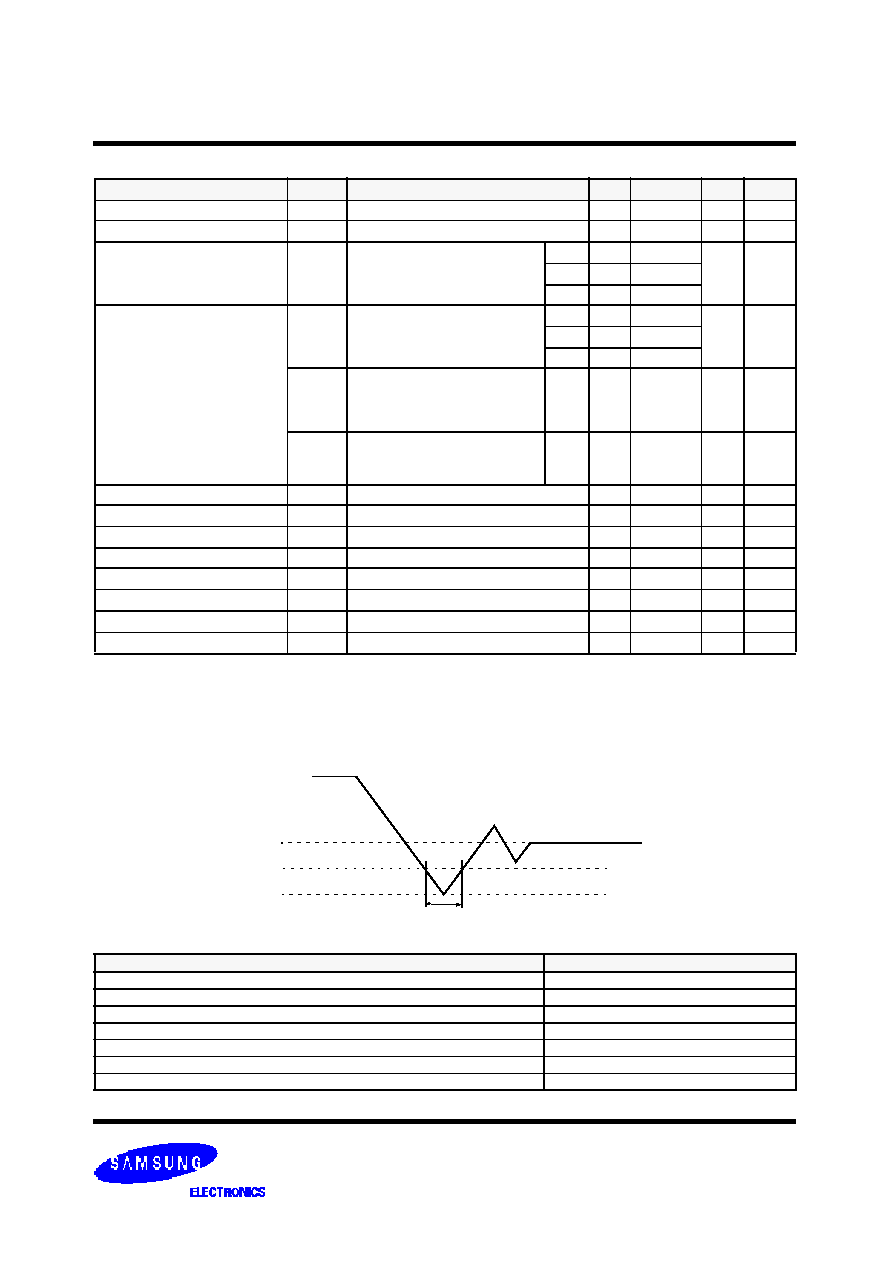
TEST CONDITIONS
* The above parameters are also guaranteed at industrial temperature range.
PARAMETER
VALUE
Input Pulse Level(for 3.3V I/O)
0 to 3.0V
Input Pulse Level(for 2.5V I/O)
0 to 2.5V
Input Rise and Fall Time(Measured at 20% to 80% for 3.3V I/O)
1.0V/ns
Input Rise and Fall Time(Measured at 20% to 80% for 2.5V I/O)
1.0V/ns
Input and Output Timing Reference Levels for 3.3V I/O
1.5V
Input and Output Timing Reference Levels for 2.5V I/O
V
DDQ
/2
Output Load
See Fig. 1
(V
DD
=3.3V+0.165V/-0.165V,V
DDQ
=3.3V+0.165/-0.165V or V
DD
=3.3V+0.165V/-0.165V,V
DDQ
=2.5V+0.4V/-0.125V, T
A
=0to70
°
C)
DC ELECTRICAL CHARACTERISTICS
(V
DD
=3.3V+0.165V/-0.165V , T
A
=0
°
C to +70
°
C)
Notes :
1. The above parameters are also guaranteed at industrial temperature range.
2. Reference AC Operating Conditions and Characteristics for input and timing.
3. Data states are all zero.
4. In Case of I/O Pins, the Max. V
IH
=V
DDQ
+0.3V.
PARAMETER
SYMBOL
TEST CONDITIONS
MIN
MAX
UNIT NOTES
Input Leakage Current(except ZZ)
I
IL
V
DD
= Max ; V
IN
=V
SS
to V
DD
-2
+2
µ
A
Output Leakage Current
I
OL
Output Disabled, V
OUT
=V
SS
to V
DDQ
-2
+2
µ
A
Operating Current
I
CC
Device Selected, I
OUT
=0mA,
ZZ
V
IL ,
Cycle Time
t
CYC
Min
-25
-
470
mA
1,2
-16
-
350
-14
-
290
Standby Current
I
SB
Device deselected, I
OUT
=0mA,
ZZ
V
IL
, f=Max,
All Inputs
0.2V or
V
DD
-0.2V
-25
-
120
mA
-16
-
90
-14
-
90
I
SB1
Device deselected, I
OUT
=0mA,
ZZ
0.2V,
f = 0, All Inputs=fixed (V
DD
-0.2V or
0.2V)
-
70
mA
I
SB2
Device deselected, I
OUT
=0mA,
ZZ
V
DD
-0.2V, f=Max, All Inputs
V
IL
or
V
IH
-
60
mA
Output Low Voltage(3.3V I/O)
V
OL
I
OL
=8.0mA
-
0.4
V
Output High Voltage(3.3V I/O)
V
OH
I
OH
=-4.0mA
2.4
-
V
Output Low Voltage(2.5V I/O)
V
OL
I
OL
=1.0mA
-
0.4
V
Output High Voltage(2.5V I/O)
V
OH
I
OH
=-1.0mA
2.0
-
V
Input Low Voltage(3.3V I/O)
V
IL
-0.3*
0.8
V
nput High Voltage(3.3V I/O)
V
IH
2.0
V
DD
+0.3**
V
3
Input Low Voltage(2.5V I/O)
V
IL
-0.3*
0.7
V
Input High Voltage(2.5V I/O)
V
IH
1.7
V
DD
+0.3**
V
3
512Kx36 & 1Mx18 Synchronous SRAM
- 10 -
Rev 3.0
Nov. 2003
K7A161800A
K7A163600A
Output Load(B),
(for t
LZC
, t
LZOE
, t
HZOE
& t
HZC
)
Dout
353
/
1538
5pF*
+3.3V for 3.3V I/O
319
/
1667
Fig. 1
* Including Scope and Jig Capacitance
Output Load(A)
Dout
Zo=50
RL=50
VL=1.5V for 3.3V I/O
V
DDQ
/2 for 2.5V I/O
/+2.5V for 2.5V I/O
30pF*
AC TIING CHARACTERISTICS
(V
DD
=3.3V+0.165V/-0.165V, T
A
=0
°
C to +70
°
C)
Notes
: 1. The above parameters are also guaranteed at industrial temperature range.
2. All address inputs must meet the specified setup and hold times for all rising clock edges whenever ADSC and/or ADSP is sampled low and CS
is sampled low. All other synchronous inputs must meet the specified setup and hold times whenever this device is chip selected.
3. Both chip selects must be active whenever ADSC or ADSP is sampled low in order for the this device to remain enabled.
4. ADSC or ADSP must not be asserted for at least 2 Clock after leaving ZZ state.
Parameter
Symbol
-25
-16
-14
Unit
MIN
MAX
Min
Max
Min
Max
Cycle Time
t
CYC
4.0
-
6.0
-
7.2
-
ns
Clock Access Time
t
CD
-
2.6
-
3.5
-
4.0
ns
Output Enable to Data Valid
t
OE
-
2.6
-
3.5
-
4.0
ns
Clock High to Output Low-Z
t
LZC
0
-
0
-
0
-
ns
Output Hold from Clock High
t
OH
1.5
-
1.5
-
1.5
-
ns
Output Enable Low to Output Low-Z
t
LZOE
0
-
0
-
0
-
ns
Output Enable High to Output High-Z
t
HZOE
-
2.6
-
3.0
-
3.5
ns
Clock High to Output High-Z
t
HZC
1.5
2.6
1.5
3.0
1.5
3.5
ns
Clock High Pulse Width
t
CH
1.7
-
2.1
-
2.5
-
ns
Clock Low Pulse Width
t
CL
1.7
-
2.1
-
2.5
-
ns
Address Setup to Clock High
t
AS
1.2
-
1.5
-
1.5
-
ns
Address Status Setup to Clock High
t
SS
1.2
-
1.5
-
1.5
-
ns
Data Setup to Clock High
t
DS
1.2
-
1.5
-
1.5
-
ns
Write Setup to Clock High (GW, BW , WE
X
)
t
WS
1.2
-
1.5
-
1.5
-
ns
Address Advance Setup to Clock High
t
ADVS
1.2
-
1.5
-
1.5
-
ns
Chip Select Setup to Clock High
t
CSS
1.2
-
1.5
-
1.5
-
ns
Address Hold from Clock High
t
AH
0.3
-
0.5
-
0.5
-
ns
Address Status Hold from Clock High
t
SH
0.3
-
0.5
-
0.5
-
ns
Data Hold from Clock High
t
DH
0.3
-
0.5
-
0.5
-
ns
Write Hold from Clock High (GW, BW, WE
X
)
t
WH
0.3
-
0.5
-
0.5
-
ns
Address Advance Hold from Clock High
t
ADVH
0.3
-
0.5
-
0.5
-
ns
Chip Select Hold from Clock High
t
CSH
0.3
-
0.5
-
0.5
-
ns
ZZ High to Power Down
t
PDS
2
-
2
-
2
-
cycle
ZZ Low to Power Up
t
PUS
2
-
2
-
2
-
cycle
512Kx36 & 1Mx18 Synchronous SRAM
- 11 -
Rev 3.0
Nov. 2003
K7A161800A
K7A163600A
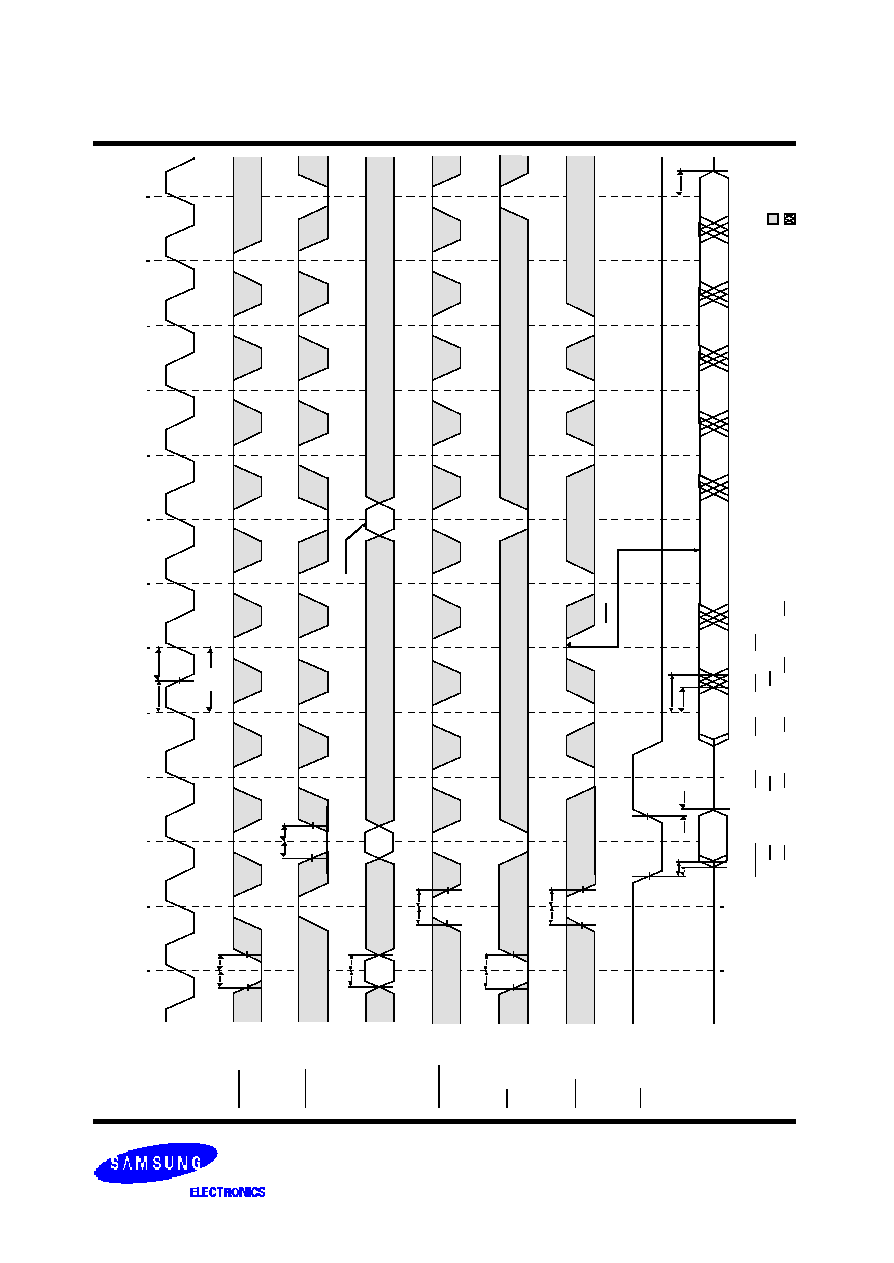
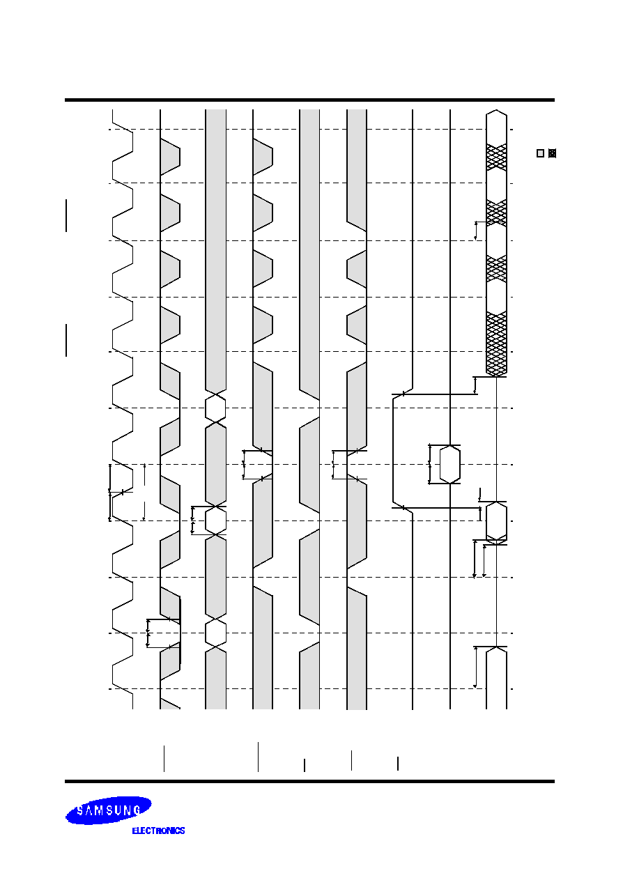
C
L
O
C
K
A
D
S
P
A
D
S
C
A
D
D
R
E
S
S
W
R
I
T
E
C
S
A
D
V
O
E
D
a
t
a
O
u
t
T
I
M
I
N
G
W
A
V
E
F
O
R
M
O
F
R
E
A
D
C
Y
C
L
E
N
O
T
E
S
:
W
R
I
T
E
=
L
m
e
a
n
s
G
W
=
L
,
o
r
G
W
=
H
,
B
W
=
L
,
W
E
x
=
L
C
S
=
L
m
e
a
n
s
C
S
1
=
L
,
C
S
2
=
H
a
n
d
C
S
2
=
L
C
S
=
H
m
e
a
n
s
C
S
1
=
H
,
o
r
C
S
1
=
L
a
n
d
C
S
2
=
H
,
o
r
C
S
1
=
L
,
a
n
d
C
S
2
=
L
t
C
H
t
C
L
t
S
S
t
S
H
t
S
S
t
S
H
t
A
S
t
A
H
A
1
A
2
A
3
B
U
R
S
T
C
O
N
T
I
N
U
E
D
W
I
T
H
N
E
W
B
A
S
E
A
D
D
R
E
S
S
t
W
S
t
W
H
t
C
S
S
t
C
S
H
t
A
D
V
S
t
A
D
V
H
t
O
E
t
H
Z
O
E
t
L
Z
O
E
t
C
D
t
O
H
(
A
D
V
I
N
S
E
R
T
S
W
A
I
T
S
T
A
T
E
)
t
H
Z
C
Q
3
-
4
Q
3
-
3
Q
3
-
2
Q
3
-
1
Q
2
-
4
Q
2
-
3
Q
2
-
2
Q
2
-
1
Q
1
-
1
D
o
n
t
C
a
r
e
U
n
d
e
f
i
n
e
d
t
C
Y
C
512Kx36 & 1Mx18 Synchronous SRAM
- 12 -
Rev 3.0
Nov. 2003
K7A161800A
K7A163600A
T
I
M
I
N
G
W
A
V
E
F
O
R
M
O
F
W
R
T
E
C
Y
C
L
E
C
L
O
C
K
A
D
S
P
A
D
S
C
A
D
D
R
E
S
S
W
R
I
T
E
C
S
A
D
V
D
a
t
a
I
n
t
C
H
t
C
L
t
S
S
t
S
H
t
A
S
t
A
H
A
1
A
2
A
3
(
A
D
S
C
E
X
T
E
N
D
E
D
B
U
R
S
T
)
D
2
-
1
D
1
-
1
t
C
S
S
t
C
S
H
(
A
D
V
S
U
S
P
E
N
D
S
B
U
R
S
T
)
D
2
-
2
D
2
-
3
D
2
-
4
D
3
-
1
D
3
-
2
D
3
-
3
D
2
-
2
D
3
-
4
Q
0
-
3
Q
0
-
4
O
E
D
a
t
a
O
u
t
t
S
S
t
S
H
t
W
S
t
W
H
t
A
D
V
S
t
A
D
V
H
t
D
S
t
D
H
t
H
Z
O
E
D
o
n
t
C
a
r
e
U
n
d
e
f
i
n
e
d
t
C
Y
C
512Kx36 & 1Mx18 Synchronous SRAM
- 13 -
Rev 3.0
Nov. 2003
K7A161800A
K7A163600A
T
I
M
I
N
G
W
A
V
E
F
O
R
M
O
F
C
O
M
B
I
N
A
T
I
O
N
R
E
A
D
/
W
R
T
E
C
Y
C
L
E
(
A
D
S
P
C
O
N
T
R
O
L
L
E
D
,
A
D
S
C
=
H
I
G
H
)
C
L
O
C
K
A
D
S
P
A
D
D
R
E
S
S
W
R
I
T
E
C
S
A
D
V
O
E
D
a
t
a
O
u
t
t
C
H
t
C
L
t
D
S
t
D
H
Q
3
-
2
D
a
t
a
I
n
t
O
H
A
1
A
2
A
3
D
2
-
1
Q
3
-
1
Q
3
-
3
t
S
S
t
S
H
t
A
S
t
A
H
t
W
S
t
W
H
t
A
D
V
S
t
A
D
V
H
t
L
Z
O
E
t
H
Z
O
E
t
C
D
t
H
Z
C
Q
3
-
4
t
L
Z
C
Q
1
-
1
D
o
n
t
C
a
r
e
U
n
d
e
f
i
n
e
d
t
C
Y
C
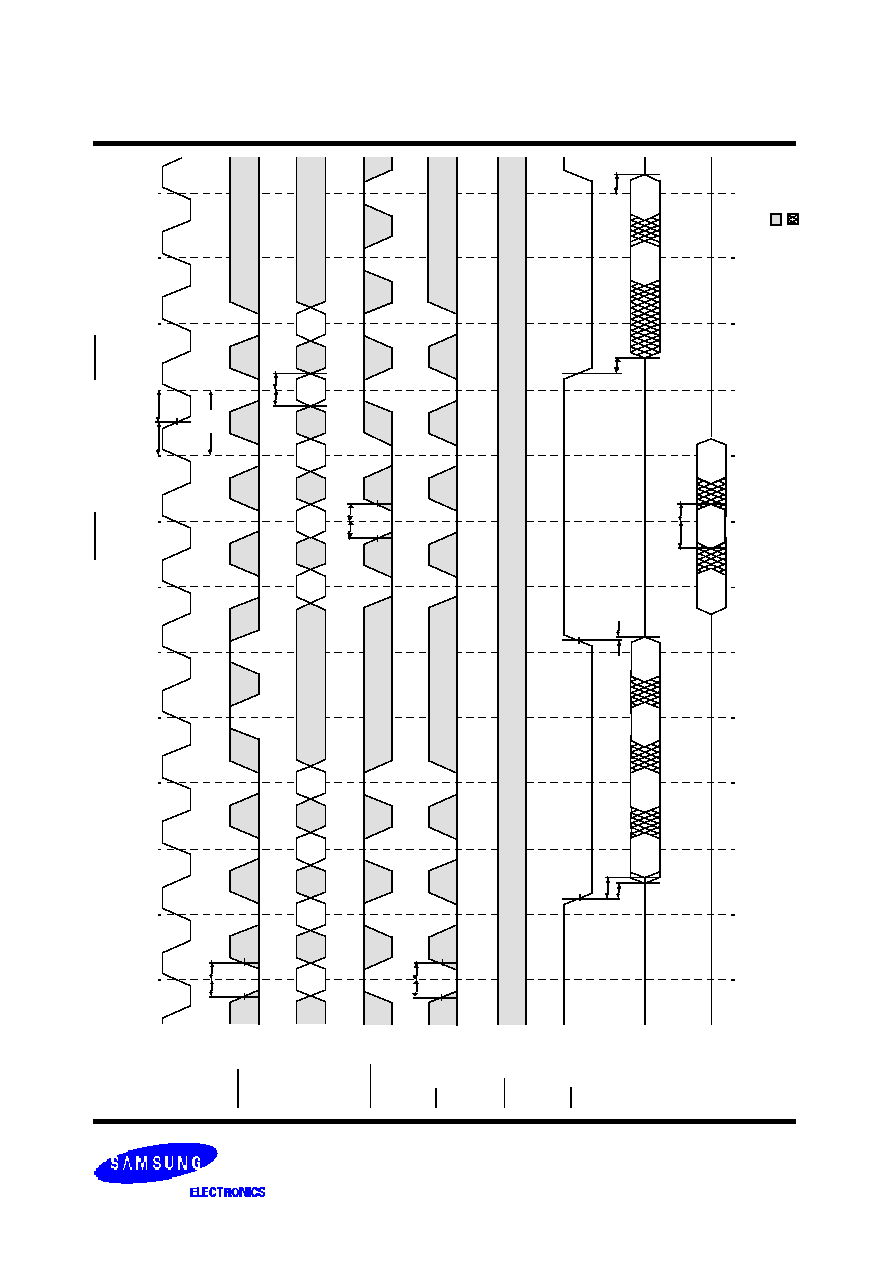
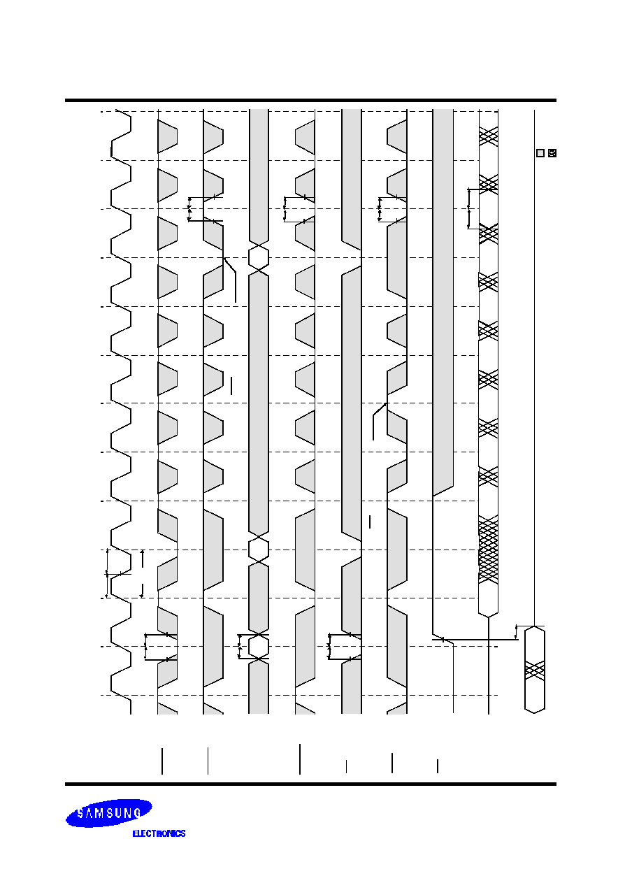
512Kx36 & 1Mx18 Synchronous SRAM
- 14 -
Rev 3.0
Nov. 2003
K7A161800A
K7A163600A
T
I
M
I
N
G
W
A
V
E
F
O
R
M
O
F
S
I
N
G
L
E
R
E
A
D
/
W
R
I
T
E
C
Y
C
L
E
(
A
D
S
C
C
O
N
T
R
O
L
L
E
D
,
A
D
S
P
=
H
I
G
H
)
C
L
O
C
K
A
D
S
C
A
D
D
R
E
S
S
W
R
I
T
E
C
S
A
D
V
O
E
D
a
t
a
I
n
t
C
H
t
C
L
t
H
Z
O
E
D
6
-
1
D
a
t
a
O
u
t
t
W
S
t
W
H
t
L
Z
O
E
t
O
H
t
O
E
D
5
-
1
D
7
-
1
t
W
S
t
W
H
t
L
Z
O
E
t
D
H
t
D
S
A
1
A
2
A
3
A
4
A
5
A
6
A
7
A
8
A
9
Q
3
-
1
Q
1
-
1
Q
2
-
1
Q
4
-
1
Q
8
-
1
t
C
S
S
t
C
S
H
t
S
S
t
S
H
Q
9
-
1
D
o
n
t
C
a
r
e
U
n
d
e
f
i
n
e
d
t
C
Y
C
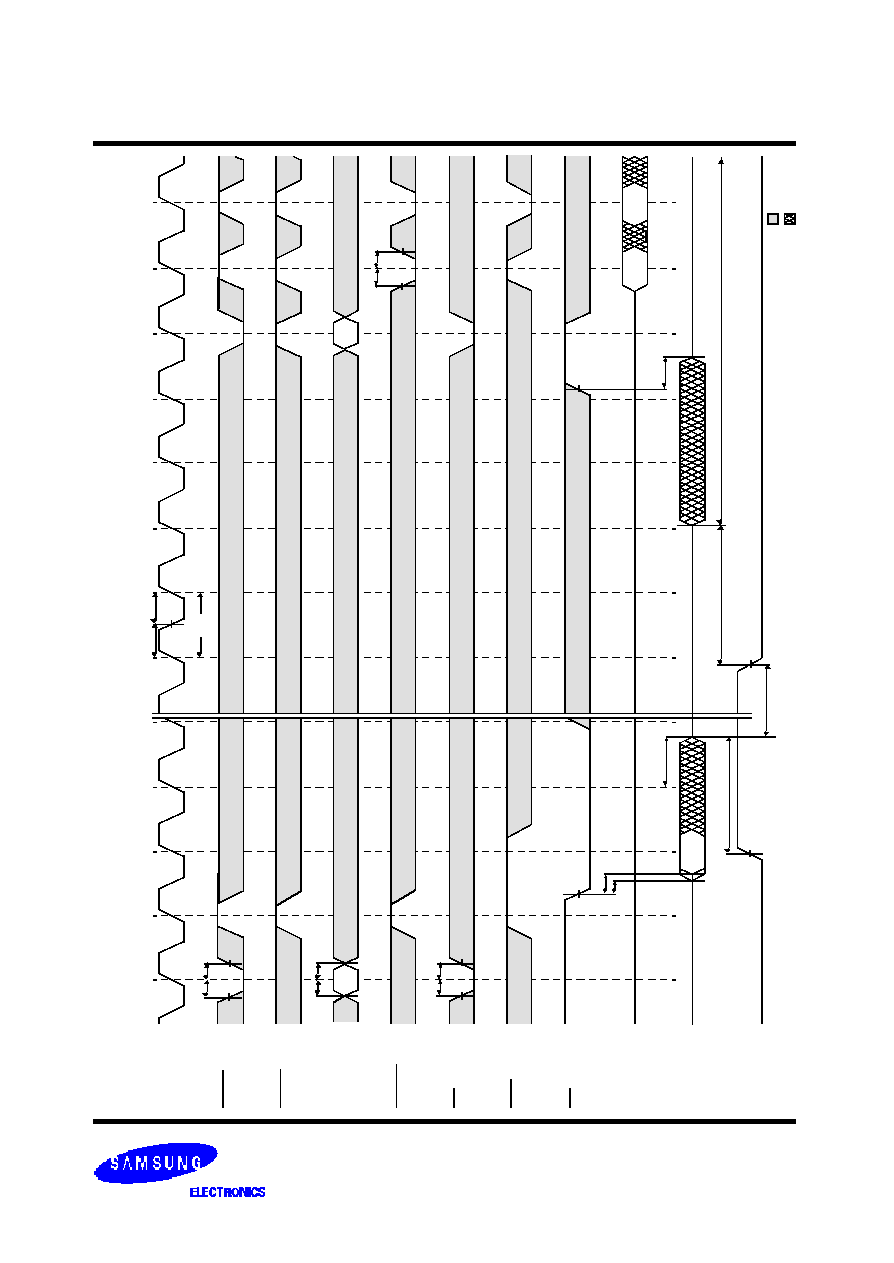
512Kx36 & 1Mx18 Synchronous SRAM
- 15 -
Rev 3.0
Nov. 2003
K7A161800A
K7A163600A
T
I
M
I
N
G
W
A
V
E
F
O
R
M
O
F
P
O
W
E
R
D
O
W
N
C
Y
C
L
E
C
L
O
C
K
A
D
S
P
A
D
D
R
E
S
S
W
R
I
T
E
C
S
A
D
V
D
a
t
a
I
n
t
C
H
t
C
L
D
2
-
2
O
E
t
H
Z
O
E
D
2
-
1
A
1
t
S
S
t
S
H
D
a
t
a
O
u
t
t
P
U
S
A
D
S
C
Z
Z
t
A
S
t
A
H
t
C
S
S
t
C
S
H
S
l
e
e
p
S
t
a
t
e
N
o
r
m
a
l
O
p
e
r
a
t
i
o
n
M
o
d
e
Z
Z
R
e
c
o
v
e
r
y
C
y
c
l
e
A
2
t
W
S
t
W
H
t
L
Z
O
E
Q
1
-
1
t
O
E
t
H
Z
C
t
P
D
S
Z
Z
S
e
t
u
p
C
y
c
l
e
D
o
n
t
C
a
r
e
U
n
d
e
f
i
n
e
d
t
C
Y
C
512Kx36 & 1Mx18 Synchronous SRAM
- 16 -
Rev 3.0
Nov. 2003
K7A161800A
K7A163600A
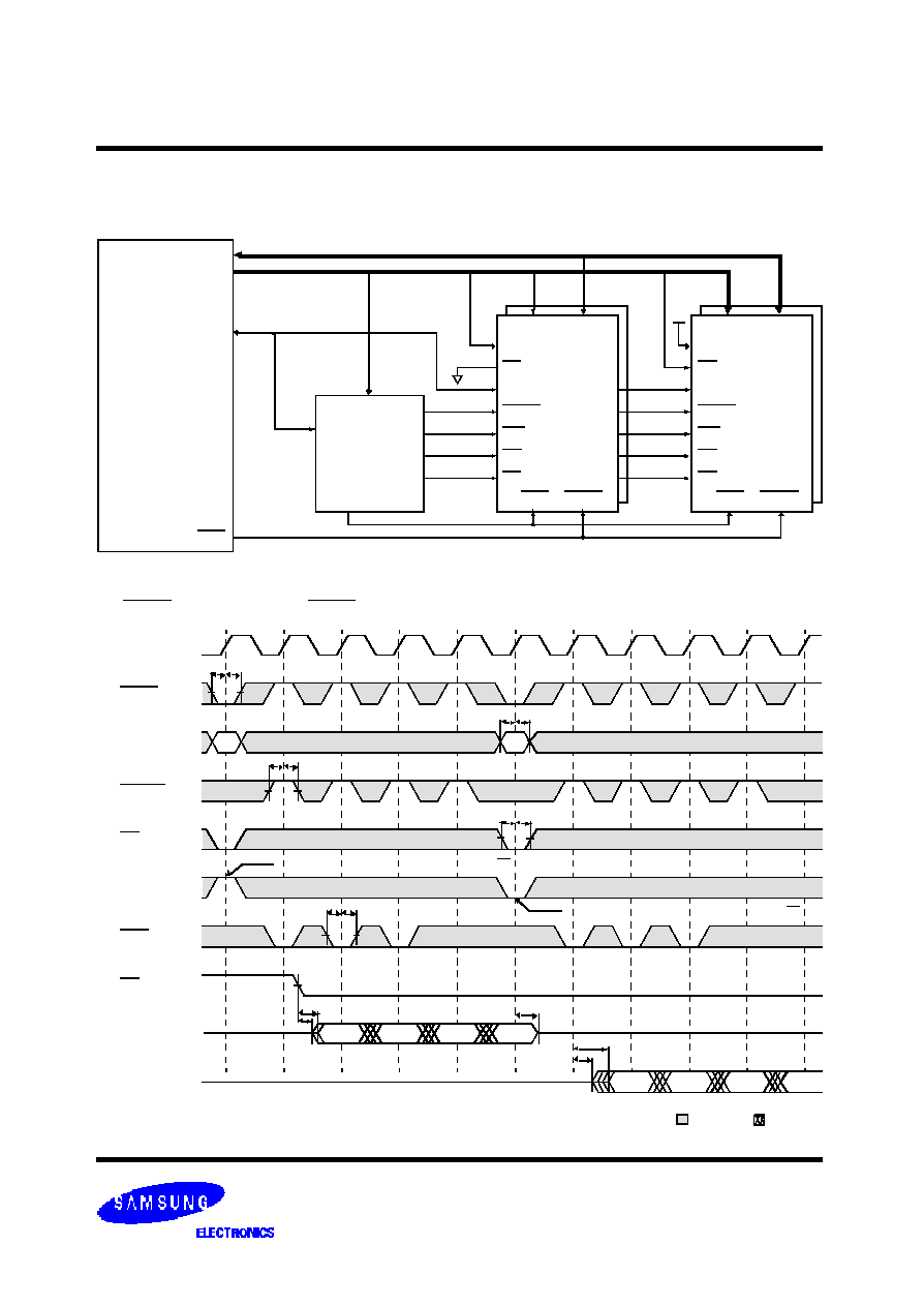
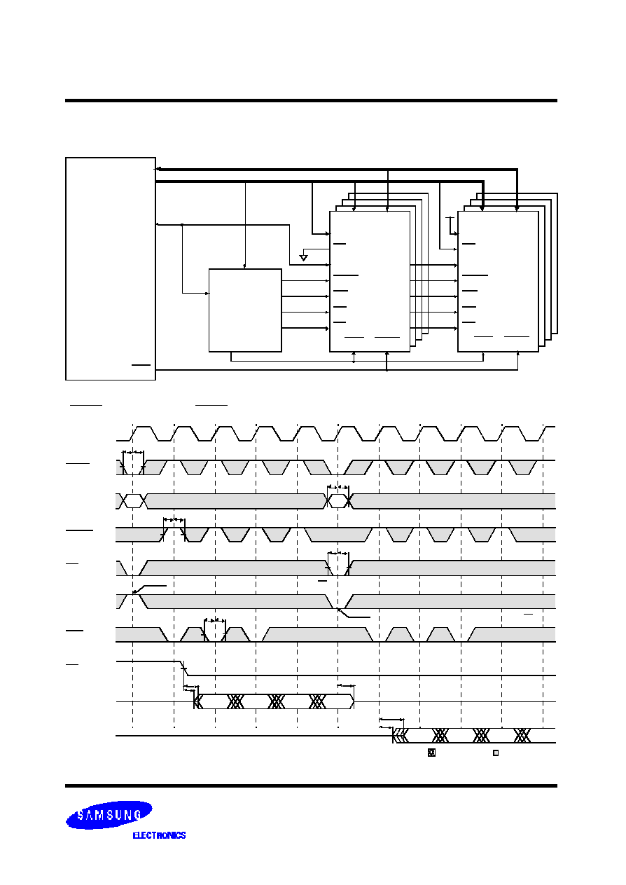
APPLICATION INFORMATION
The Samsung 512Kx36 Synchronous Pipelined Burst SRAM has two additional chip selects for simple depth expansion.
DEPTH EXPANSION
This permits easy secondary cache upgrades from 512K depth to 1M depth without extra logic.
Data
Address
CLK
ADS
CS
2
CS
2
CLK
ADSC
WEx
OE
CS
1
Address Data
ADV ADSP
512Kx36
SPB
SRAM
(Bank 0)
CS
2
CS
2
CLK
ADSC
WEx
OE
CS
1
Address Data
ADV ADSP
512Kx36
SPB
SRAM
(Bank 1)
CLK
Address
Cache
Controller
A
[0:19]
A
[19]
A
[0:18]
A
[19]
A
[0:18]
I/O
[0:71]
Microprocessor
Clock
ADSP
ADDRESS
Data Out
Bank 0 is selected by CS
2
, and Bank 1 deselected by CS
2
Q1-1
Q1-2
Q1-4
Q1-3
OE
Data Out
t
SS
t
SH
A1
A2
WRITE
CS
1
A
n+1
ADV
(Bank 0)
(Bank 1)
Q2-2
Q2-4
Q2-3
t
AS
t
AH
t
WS
t
WH
t
ADVS
t
ADVH
t
OE
t
LZOE
t
HZC
Bank 0 is deselected by CS
2
, and Bank 1 selected by CS
2
t
CSS
t
CSH
t
CD
t
LZC
[0:n]
Q2-1
INTERLEAVE READ TIMING
(Refer to non-interleave write timing for interleave write timing)
Don
t Care
Undefined
(ADSP CONTROLLED , ADSC=HIGH)
*Notes :
n = 14 32K depth , 15 64K depth
16 128K depth , 17 256K depth
18 512K depth , 19 1M depth
512Kx36 & 1Mx18 Synchronous SRAM
- 17 -
Rev 3.0
Nov. 2003
K7A161800A
K7A163600A
APPLICATION INFORMATION
DEPTH EXPANSION
Data
Address
CLK
ADS
Microprocessor
CS
2
CS
2
CLK
ADSC
WEx
OE
CS
1
Address Data
ADV ADSP
1Mx18
SPB
SRAM
(Bank 0)
CS
2
CS
2
CLK
ADSC
WEx
OE
CS
1
Address Data
ADV ADSP
1Mx18
SPB
SRAM
(Bank 1)
CLK
Address
Cache
Controller
A
[0:20]
A
[20]
A
[0:19]
A
[20]
A
[0:19]
I/O
[0:71]
Clock
ADSP
ADDRESS
Data Out
Bank 0 is selected by CS
2
, and Bank 1 deselected by CS
2
Q1-1
Q1-2
Q1-4
Q1-3
OE
Data Out
t
SS
tSH
Don
t Care
A1
A2
WRITE
CS
1
A
n+1
ADV
(Bank 0)
(Bank 1)
Q2-2
Q2-4
Q2-3
t
AS
t
AH
t
WS
t
WH
t
ADVS
t
ADVH
t
OE
t
LZOE
tHZC
Bank 0 is deselected by CS
2
, and Bank 1 selected by CS
2
t
CSS
tCSH
t
CD
t
LZC
[0:n]
Undefined
Q2-1
INTERLEAVE READ TIMING
(Refer to non-interleave write timing for interleave write timing)
(ADSP CONTROLLED , ADSC=HIGH)
The Samsung 1Mx18 Synchronous Pipelined Burst SRAM has two additional chip selects for simple depth expansion.
This permits easy secondary cache upgrades from 1M depth to 2M depth without extra logic.
*Notes :
n = 14 32K depth , 15 64K depth
16 128K depth , 17 256K depth
18 512K depth , 19 1M depth
20 2M depth
512Kx36 & 1Mx18 Synchronous SRAM
- 18 -
Rev 3.0
Nov. 2003
K7A161800A
K7A163600A
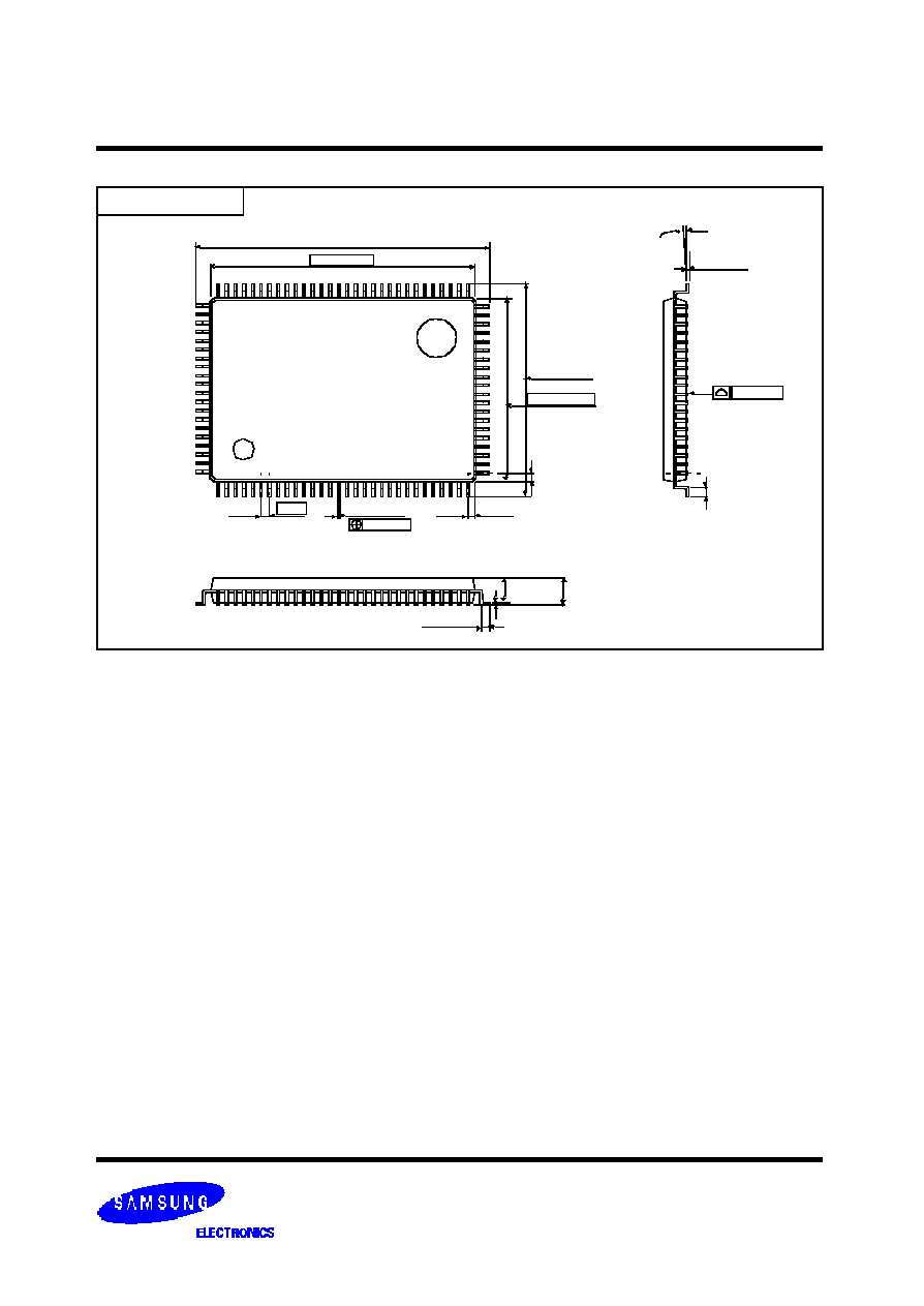
PACKAGE DIMENSIONS
0.10 MAX
0~8
°
22.00
±
0.30
20.00
±
0.20
16.00
±
0.30
14.00
±
0.20
1.40
±
0.10
1.60 MAX
0.05 MIN
(0.58)
0.50
±
0.10
#1
(0.83)
0.50
±
0.10
100-TQFP-1420A
0.65
0.30
±
0.10
0.10 MAX
+ 0.10
- 0.05
0.127
Units ; millimeters/Inches