
K7B321825M
1Mx36 & 2Mx18 Synchronous SRAM
- 1 -
Rev 1.1
Oct. 2003
K7B323625M
Document Title
1Mx36 & 2Mx18-Bit Synchronous Burst SRAM
The attached data sheets are prepared and approved by SAMSUNG Electronics. SAMSUNG Electronics CO., LTD. reserve the right to change the
specifications. SAMSUNG Electronics will evaluate and reply to your requests and questions on the parameters of this device. If you have any ques-
tions, please contact the SAMSUNG branch office near your office, call or contact Headquarters.
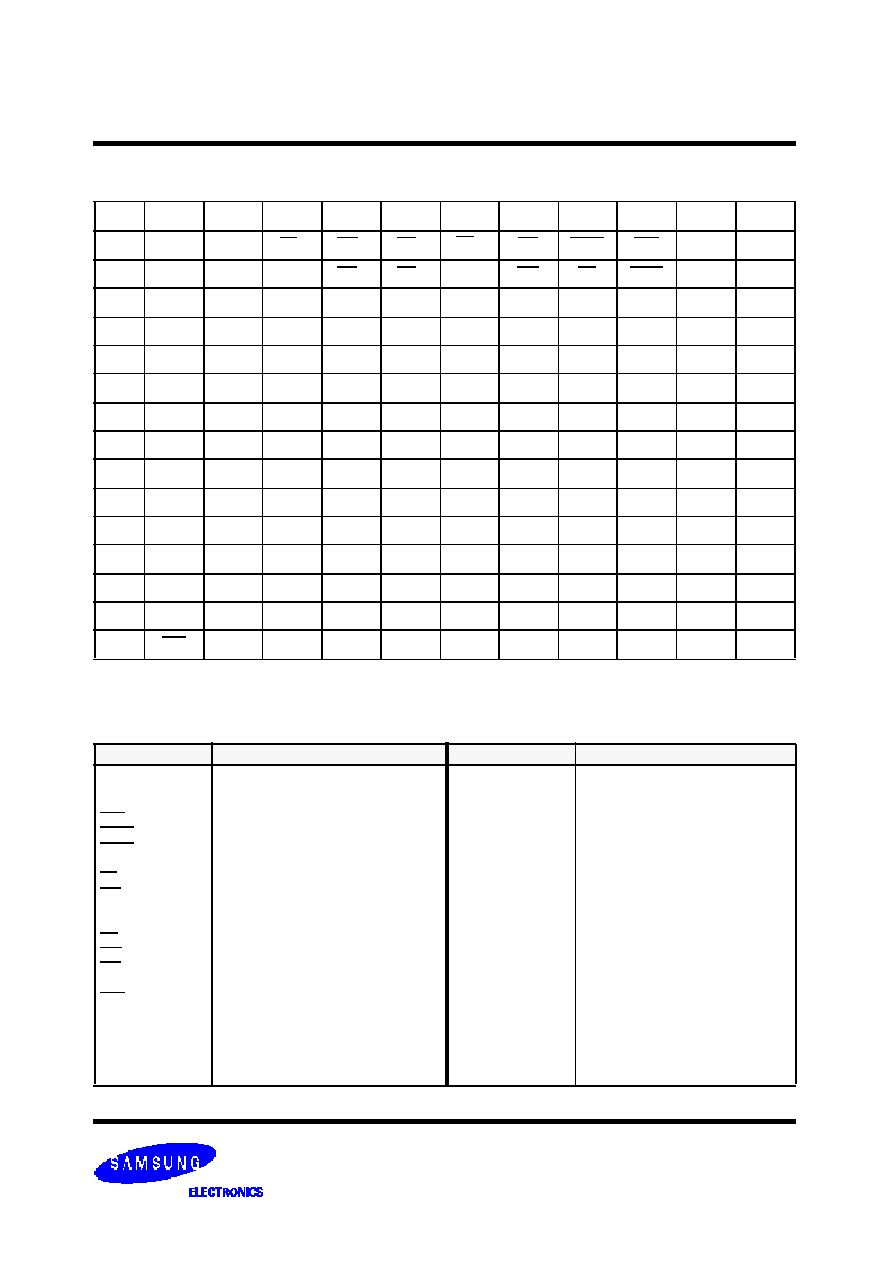
Revision History
Rev. No.
0.0
0.1
0.2
0.3
0.4
0.5
1.0
1.1
Remark
Advance
Preliminary
Preliminary
Preliminary
Preliminary
Preliminary
Final
Final
History
1. Initial draft
1. Add 165FBGA package
1. Update JTAG scan order
1. Change pin out for 165FBGA
- x18/x36 ; 11B => from A to NC , 2R ==> from NC to A .
1. Insert pin at JTAG scan order of 165FBGA in connection with
pin out change
- x18/x36 ; insert Pin ID of 2R to BIT number of 69
1. Add Icc, Isb, Isb1 and Isb2 values.
1. Correct the pin name of 100TQFP.
1. Change the Stand-by current (Isb)
Before After
Isb - 65 : 100 140
- 75 : 90 130
- 85 : 80 130
Isb1 : 90 110
Isb2 : 80 100
Draft Date
May. 10. 2001
Aug. 29. 2001
Dec. 03. 2001
Feb. 14 . 2002
Apr. 20. 2002
May. 10. 2002
Oct. 15. 2002
Oct. 17, 2003
K7B321825M
1Mx36 & 2Mx18 Synchronous SRAM
- 2 -
Rev 1.1
Oct. 2003
K7B323625M
32Mb SB/SPB Synchronous SRAM
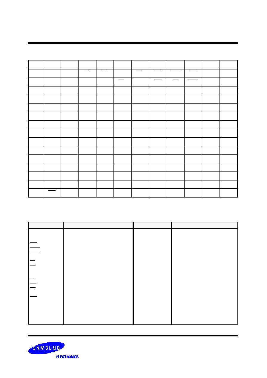
Ordering Information
Org.
Part Number
Mode
VDD
Speed
SB ; Access Time(ns)
SPB ; Cycle Time(MHz)
PKG
Temp
2Mx18
K7B321825M-Q(H/F)C65/75/85
SB
3.3
6.5/7.5/8.5ns
Q: 100TQFP
H: 119BGA
F: 165FBGA
C
(Commercial
Temperature
Range)
K7A321800M-Q(H/F)C25/22/20/16/15/14 SPB(2E1D)
3.3
250/225/200/167/150/138MHz
K7A321801M-QC25/22/20/16/15/14
SPB(2E2D)
3.3
250/225/200/167/150/138MHz
1Mx36
K7B323625M-Q(H/F)C65/75/85
SB
3.3
6.5/7.5/8.5ns
K7A323600M-Q(H/F)C25/22/20/16/15/14 SPB(2E1D)
3.3
250/225/200/167/150/138MHz
K7A323601M-QC25/22/20/16/15/14
SPB(2E2D)
3.3
250/225/200/167/150/138MHz
K7B321825M
1Mx36 & 2Mx18 Synchronous SRAM
- 3 -
Rev 1.1
Oct. 2003
K7B323625M
1Mx36 & 2Mx18-Bit Synchronous Burst SRAM
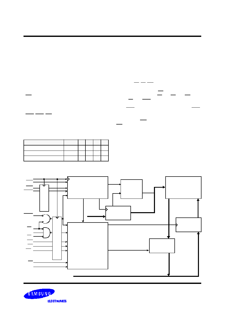
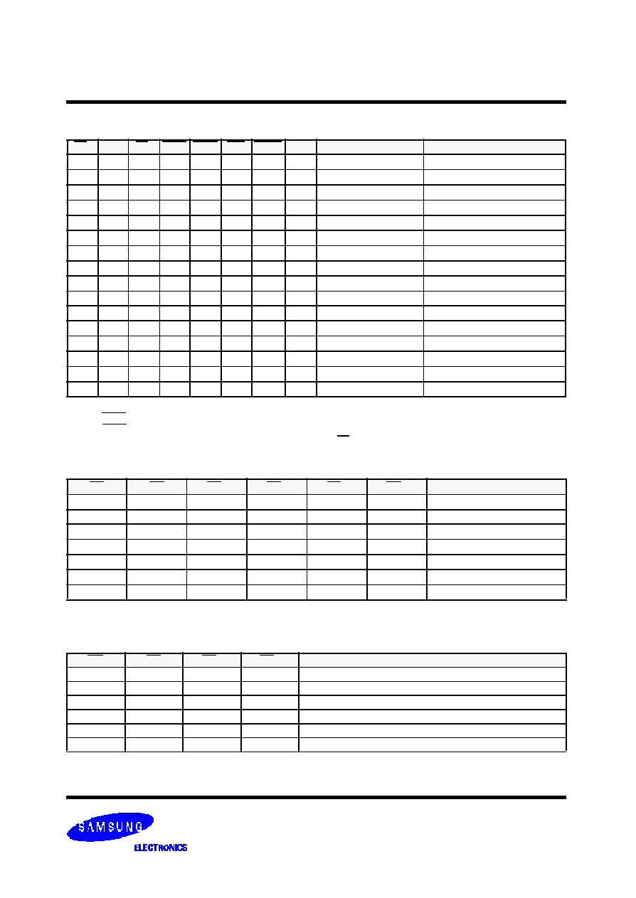
The K7B323625M and K7B321825M are 37,748,736-bit Syn-
chronous Static Random Access Memory designed for high
performance second level cache of Pentium and Power PC
based System.
It is organized as 1M(2M) words of 36(18) bits and integrates
address and control registers, a 2-bit burst address counter and
added some new functions for high performance cache RAM
applications; G W, B W, LBO, ZZ. Write cycles are internally self-
timed and synchronous.
Full bus-width write is done by GW, and each byte write is per-
formed by the combination of W Ex and BW when G W is high.
And with CS
1
high, ADSP is blocked to control signals.
Burst cycle can be initiated with either the address status pro-
cessor(ADSP) or address status cache controller(ADSC)
inputs. Subsequent burst addresses are generated internally in
the system
s burst sequence and are controlled by the burst
address advance(ADV) input.
LBO pin is DC operated and determines burst sequence(linear
or interleaved).
ZZ pin controls Power Down State and reduces Stand-by cur-
rent regardless of CLK.
The K7B323625M and K7B321825M are fabricated using SAM-
SUNG
s high performance CMOS technology and is available
in a 100pin TQFP, 119BGA and 165FBGA package. Multiple
power and ground pins are utilized to minimize ground bounce.
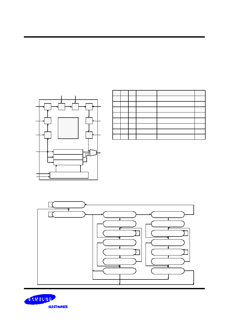
GENERAL DESCRIPTION
FEATURES
LOGIC BLOCK DIAGRAM
∑
Synchronous Operation.
∑
On-Chip Address Counter.
∑
Self-Timed Write Cycle.
∑
On-Chip Address and Control Registers.
∑
3.3V+0.165V/-0.165V Power Supply.
∑ I/O Supply Voltage 3.3V+0.165V/-0.165V for 3.3V I/O
or 2.5V+0.4V/-0.125V for 2.5V I/O
∑
5V Tolerant Inputs Except I/O Pins.
∑
Byte Writable Function.
∑
Global Write Enable Controls a full bus-width write.
∑
Power Down State via ZZ Signal.
∑
LBO Pin allows a choice of either a interleaved burst or a lin-
ear burst.
∑
Three Chip Enables for simple depth expansion with No Data
Contention only for TQFP.
∑
Asynchronous Output Enable Control.
∑
ADSP, ADSC, ADV Burst Control Pins.
∑
TTL-Level Three-State Output.
∑
100-TQFP-1420A /119BGA(7x17 Ball Grid Array Package)
∑ 165FBGA(11x15 ball aray) with body size of 15mmx17mm.
CLK
LBO
ADV
ADSC
ADSP
CS
1
CS
2
CS
2
GW
BW
WEx
OE
ZZ
DQa
0
~ DQd
7
or DQa0 ~ DQb7
BURST CONTROL
LOGIC
BURST
1Mx36 , 2Mx18
ADDRESS
CONTROL
DATA-IN
ADDRESS
COUNTER
MEMORY
ARRAY
REGISTER
REGISTER
LOGIC
C
O
N
T
R
O
L
R
E
G
I
S
T
E
R
C
O
N
T
R
O
L
R
E
G
I
S
T
E
R
A
0
~A
1
A
0
~A
1
or A
2
~A
20
or A
0
~A
20
DQPa ~ DQPd
A
0
~A
19
A
2
~A
19
(x=a,b,c,d or a,b)
DQPa,DQPb
OUTPUT
BUFFER
FAST ACCESS TIMES
PARAMETER
Symbol
-65 -75 -85 Unit
Cycle Time
t
CYC
7.5 8.5
10
ns
Clock Access Time
t
CD
6.5 7.5 8.5
ns
Output Enable Access Time
t
OE
3.5 3.5 4.0
ns

K7B321825M
1Mx36 & 2Mx18 Synchronous SRAM
- 4 -
Rev 1.1
Oct. 2003
K7B323625M
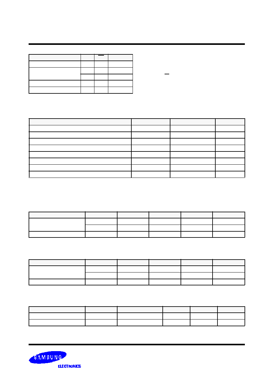
PIN CONFIGURATION
(TOP VIEW)
PIN NAME
Notes :
1. A
0
and A
1
are the two least significant bits(LSB) of the address field and set the internal burst counter if burst is desired.
SYMBOL
PIN NAME
TQFP PIN NO.
SYMBOL
PIN NAME
TQFP PIN NO.
A
0
- A
19
ADV
ADSP
ADSC
CLK
CS
1
CS
2
CS
2
WE x(x=a,b,c,d)
OE
G W
BW
ZZ
LBO
Address Inputs
Burst Address Advance
Address Status Processor
Address Status Controller
Clock
Chip Select
Chip Select
Chip Select
Byte Write Inputs
Output Enable
Global Write Enable
Byte Write Enable
Power Down Input
Burst Mode Control
32,33,34,35,36,37,39
42,43,44,45,46,47,48,
49,50,81,82,99,100
83
84
85
89
98
97
92
93,94,95,96
86
88
87
64
31
V
DD
V
SS
N.C.
DQa
0
~a
7
DQb
0
~b
7
DQc
0
~c
7
DQd
0
~d
7
DQPa~P
d
V
DDQ
V
SSQ
Power Supply(+3.3V)
Ground
No Connect
Data Inputs/Outputs
Output Power Supply
(2.5V or 3.3V)
Output Ground
15,41,65,91
17,40,67,90
14,16,38,66
52,53,56,57,58,59,62,63
68,69,72,73,74,75,78,79
2,3,6,7,8,9,12,13
18,19,22,23,24,25,28,29
51,80,1,30
4,11,20,27,54,61,70,77
5,10,21,26,55,60,71,76
1
2
3
4
5
6
7
8
9
10
11
12
13
14
15
16
17
18
19
20
21
22
23
24
25
26
27
28
29
30
100 Pin TQFP
(20mm x 14mm)
DQPc
DQc
0
DQc
1
V
DDQ
V
SSQ
DQc
2
DQc
3
DQc
4
DQc
5
V
SSQ
V
DDQ
DQc
6
DQc
7
N.C.
V
DD
N.C.
V
SS
DQd
0
DQd
1
V
DDQ
V
SSQ
DQd
2
DQd
3
DQd
4
DQd
5
V
SSQ
V
DDQ
DQd
6
DQd
7
DQPd
80
79
78
77
76
75
74
73
72
71
70
69
68
67
66
65
64
63
62
61
60
59
58
57
56
55
54
53
52
51
DQPb
DQb
7
DQb
6
V
DDQ
V
SSQ
DQb
5
DQb
4
DQb
3
DQb
2
V
SSQ
V
DDQ
DQb
1
DQb
0
V
SS
N.C.
V
DD
ZZ
DQa
7
DQa
6
V
DDQ
V
SSQ
DQa
5
DQa
4
DQa
3
DQa
2
V
SSQ
V
DDQ
DQa
1
DQa
0
DQPa
1
0
0
9
9
9
8
9
7
9
6
9
5
9
4
9
3
9
2
9
1
9
0
8
9
8
8
8
7
8
6
8
5
8
4
8
3
8
2
A
6
A
7
C
S
1
C
S
2
W
E
d
W
E
c
W
E
b
W
E
a
C
S
2
V
D
D
V
S
S
C
L
K
G
W
B
W
O
E
A
D
S
C
A
D
S
P
A
D
V
A
8
8
1
A
9
5
0
4
9
4
8
4
7
4
6
4
5
4
4
4
3
4
2
4
1
4
0
3
9
3
8
3
7
3
6
3
5
3
4
3
3
3
2
A
1
5
A
1
4
A
1
3
A
1
2
A
1
1
A
1
0
A
1
7
A
1
8
V
D
D
V
S
S
A
1
9
N
.
C
.
A
0
A
1
A
2
A
3
A
4
A
5
3
1
L
B
O
A
1
6
K7B323625M(1Mx36)

K7B321825M
1Mx36 & 2Mx18 Synchronous SRAM
- 5 -
Rev 1.1
Oct. 2003
K7B323625M
PIN CONFIGURATION
(TOP VIEW)
PIN NAME
Notes :
1. A
0
and A
1
are the two least significant bits(LSB) of the address field and set the internal burst counter if burst is desired.
SYMBOL
PIN NAME
TQFP PIN NO.
SYMBOL
PIN NAME
TQFP PIN NO.
A
0
- A
20
ADV
ADSP
ADSC
CLK
CS
1
CS
2
CS
2
W Ex(x=a,b)
OE
G W
B W
ZZ
LBO
Address Inputs
Burst Address Advance
Address Status Processor
Address Status Controller
Clock
Chip Select
Chip Select
Chip Select
Byte Write Inputs
Output Enable
Global Write Enable
Byte Write Enable
Power Down Input
Burst Mode Control
32,33,34,35,36,37,39
42,43,44,45,46,47,48,
49,50 80,81,82,99,100
83
84
85
89
98
97
92
93,94
86
88
87
64
31
V
DD
V
SS
N.C.
DQa
0
~ a
7
DQb
0
~ b
7
DQPa, Pb
V
DDQ
V
SSQ
Power Supply(+3.3V)
Ground
No Connect
Data Inputs/Outputs
Output Power Supply
(2.5V or 3.3V)
Output Ground
15,41,65,91
17,40,67,90
1,2,3,6,7,14,16,25,28,29,
30,38,51,52,53,56,57,66,
75,78,79,95,96
58,59,62,63,68,69,72,73
8,9,12,13,18,19,22,23
74,24
4,11,20,27,54,61,70,77
5,10,21,26,55,60,71,76
1
2
3
4
5
6
7
8
9
10
11
12
13
14
15
16
17
18
19
20
21
22
23
24
25
26
27
28
29
30
100 Pin TQFP
(20mm x 14mm)
N.C.
N.C.
N.C.
V
DDQ
V
SSQ
N.C.
N.C.
DQb
0
DQb
1
V
SSQ
V
DDQ
DQb
2
DQb
3
N.C.
V
DD
N.C.
V
SS
DQb
4
DQb
5
V
DDQ
V
SSQ
DQb
6
DQb
7
DQPb
N.C.
V
SSQ
V
DDQ
N.C.
N.C.
N.C.
80
79
78
77
76
75
74
73
72
71
70
69
68
67
66
65
64
63
62
61
60
59
58
57
56
55
54
53
52
51
N.C.
N.C.
V
DDQ
V
SSQ
N.C.
DQPa
DQa
7
DQa
6
V
SSQ
V
DDQ
DQa
5
DQa
4
V
SS
N.C.
V
DD
ZZ
DQa
3
DQa
2
V
DDQ
V
SSQ
DQa
1
DQa
0
N.C.
N.C.
V
SSQ
V
DDQ
N.C.
N.C.
N.C.
1
0
0
9
9
9
8
9
7
9
6
9
5
9
4
9
3
9
2
9
1
9
0
8
9
8
8
8
7
8
6
8
5
8
4
8
3
8
2
A
6
A
7
C
S
1
C
S
2
N
.
C
.
N
.
C
.
W
E
b
W
E
a
C
S
2
V
D
D
V
S
S
C
L
K
G
W
B
W
O
E
A
D
S
C
A
D
S
P
A
D
V
A
8
8
1
A
9
5
0
4
9
4
8
4
7
4
6
4
5
4
4
4
3
4
2
4
1
4
0
3
9
3
8
3
7
3
6
3
5
3
4
3
3
3
2
A
1
5
A
1
4
A
1
3
A
1
2
A
1
1
A
1
8
A
1
9
V
D
D
V
S
S
A
2
0
N
.
C
.
A
0
A
1
A
2
A
3
A
4
A
5
3
1
L
B
O
A
1
6
K7B321825M(2Mx18)
A
1
7
A
10
K7B321825M
1Mx36 & 2Mx18 Synchronous SRAM
- 6 -
Rev 1.1
Oct. 2003
K7B323625M
119BGA PACKAGE PIN CONFIGURATIONS
(TOP VIEW)
K7B323625M(1Mx36)
Note :
* A
0
and A
1
are the two least significant bits(LSB) of the address field and set the internal burst counter if burst is desired.
1
2
3
4
5
6
7
A
V
DDQ
A
A
ADSP
A
A
V
DDQ
B
NC
A
A
ADSC
A
A
NC
C
NC
A
A
V
DD
A
A
NC
D
DQc
DQPc
V
SS
NC
V
SS
DQPb
DQb
E
DQc
DQc
V
SS
CS
1
V
SS
DQb
DQb
F
V
DDQ
DQc
V
SS
OE
V
SS
DQb
V
DDQ
G
DQc
DQc
WEc
ADV
WEb
DQb
DQb
H
DQc
DQc
V
SS
GW
V
SS
DQb
DQb
J
V
DDQ
V
DD
NC
V
DD
NC
V
DD
V
DDQ
K
DQd
DQd
V
SS
CLK
V
SS
DQa
DQa
L
DQd
DQd
WEd
NC
WEa
DQa
DQa
M
V
DDQ
DQd
V
SS
BW
V
SS
DQa
V
DDQ
N
DQd
DQd
V
SS
A
1
*
V
SS
DQa
DQa
P
DQd
DQPd
V
SS
A
0
*
V
SS
DQPa
DQa
R
NC
A
LBO
V
DD
NC
A
NC
T
NC
NC
A
A
A
A
ZZ
U
V
DDQ
TMS
TDI
TCK
TDO
NC
V
DDQ
PIN NAME
SYMBOL
PIN NAME
SYMBOL
PIN NAME
A
A
0
, A
1
ADV
ADSP
ADSC
CLK
CS
1
WE x
(x=a,b,c,d)
OE
G W
BW
ZZ
LBO
TCK
TMS
TDI
TDO
Address Inputs
Burst Count Address
Burst Address Advance
Address Status Processor
Address Status Controller
Clock
Chip Select
Byte Write Inputs
Output Enable
Global Write Enable
Byte Write Enable
Power Down Input
Burst Mode Control
JTAG Test Clock
JTAG Test Mode Select
JTAG Test Data Input
JTAG Test Data Output
V
DD
V
SS
N.C.
DQa
DQb
DQc
DQd
DQPa~Pd
V
DDQ
Power Supply(+3.3V)
Ground
No Connect
Data Inputs/Outputs
Data Inputs/Outputs
Data Inputs/Outputs
Data Inputs/Outputs
Data Inputs/Outpus
Output Power Supply
(2.5V or 3.3V)
K7B321825M
1Mx36 & 2Mx18 Synchronous SRAM
- 7 -
Rev 1.1
Oct. 2003
K7B323625M
K7B321825M(2Mx18)
Note :
* A
0
and A
1
are the two least significant bits(LSB) of the address field and set the internal burst counter if burst is desired.
1
2
3
4
5
6
7
A
V
DDQ
A
A
ADSP
A
A
V
DDQ
B
NC
A
A
ADSC
A
A
NC
C
NC
A
A
V
DD
A
A
NC
D
DQb
NC
V
SS
NC
V
SS
DQPa
NC
E
NC
DQb
V
SS
CS
1
V
SS
NC
DQa
F
V
DDQ
NC
V
SS
OE
V
SS
DQa
V
DDQ
G
NC
DQb
WE b
ADV
V
SS
NC
DQa
H
DQb
NC
V
SS
GW
V
SS
DQa
NC
J
V
DDQ
V
DD
NC
V
DD
NC
V
DD
V
DDQ
K
NC
DQb
V
SS
CLK
V
SS
NC
DQa
L
DQb
NC
V
SS
NC
W Ea
DQa
NC
M
V
DDQ
DQb
V
SS
BW
V
SS
NC
V
DDQ
N
DQb
NC
V
SS
A
1
*
V
SS
DQa
NC
P
NC
DQPb
V
SS
A
0
*
V
SS
NC
DQa
R
NC
A
LBO
V
DD
NC
A
NC
T
NC
A
A
A
A
A
ZZ
U
V
DDQ
TMS
TDI
TCK
TDO
NC
V
DDQ
119BGA PACKAGE PIN CONFIGURATIONS
(TOP VIEW)
PIN NAME
SYMBOL
PIN NAME
SYMBOL
PIN NAME
A
A
0
,A
1
ADV
ADSP
ADSC
CLK
CS
1
WEx
(x=a,b)
OE
GW
BW
ZZ
LBO
TCK
TMS
TDI
TDO
Address Inputs
Burst Count Address
Burst Address Advance
Address Status Processor
Address Status Controller
Clock
Chip Select
Byte Write Inputs
Output Enable
Global Write Enable
Byte Write Enable
Power Down Input
Burst Mode Control
JTAG Test Clock
JTAG Test Mode Select
JTAG Test Data Input
JTAG Test Data Output
V
DD
V
SS
N.C.
DQa
DQb
DQPa~Pb
V
DDQ
Power Supply(+3.3V)
Ground
No Connect
Data Inputs/Outputs
Data Inputs/Outputs
Data Inputs/Outpus
Output Power Supply
(2.5V or 3.3V)
K7B321825M
1Mx36 & 2Mx18 Synchronous SRAM
- 8 -
Rev 1.1
Oct. 2003
K7B323625M
165-PIN FBGA PACKAGE CONFIGURATIONS
(TOP VIEW)
K7B323625M(1Mx36)
Note :
* A
0
and A
1
are the two least significant bits(LSB) of the address field and set the internal burst counter if burst is desired.
1
2
3
4
5
6
7
8
9
10
11
A
NC
A
CS 1
WE c
WEb
CS2
BW
ADSC
ADV
A
NC
B
NC
A
CS2
WEd
WEa
CLK
GW
OE
ADSP
A
NC
C
DQPc
NC
V
DDQ
V
SS
V
SS
V
SS
V
SS
V
SS
V
DDQ
NC
DQPb
D
DQc
DQc
V
DDQ
V
DD
V
SS
V
SS
V
SS
V
DD
V
DDQ
DQb
DQb
E
DQc
DQc
V
DDQ
V
DD
V
SS
V
SS
V
SS
V
DD
V
DDQ
DQb
DQb
F
DQc
DQc
V
DDQ
V
DD
V
SS
V
SS
V
SS
V
DD
V
DDQ
DQb
DQb
G
DQc
DQc
V
DDQ
V
DD
V
SS
V
SS
V
SS
V
DD
V
DDQ
DQb
DQb
H
NC
V
SS
NC
V
DD
V
SS
V
SS
V
SS
V
DD
NC
NC
ZZ
J
DQd
DQd
V
DDQ
V
DD
V
SS
V
SS
V
SS
V
DD
V
DDQ
DQa
DQa
K
DQd
DQd
V
DDQ
V
DD
V
SS
V
SS
V
SS
V
DD
V
DDQ
DQa
DQa
L
DQd
DQd
V
DDQ
V
DD
V
SS
V
SS
V
SS
V
DD
V
DDQ
DQa
DQa
M
DQd
DQd
V
DDQ
V
DD
V
SS
V
SS
V
SS
V
DD
V
DDQ
DQa
DQa
N
DQPd
NC
V
DDQ
V
SS
NC
A
V
SS
V
SS
V
DDQ
NC
DQPa
P
NC
NC
A
A
TDI
A
1
*
TDO
A
A
A
A
R
LBO
A
A
A
TMS
A
0
*
TCK
A
A
A
A
PIN NAME
SYMBOL
PIN NAME
SYMBOL
PIN NAME
A
A
0
, A
1
ADV
ADSP
ADSC
CLK
CS
1
WE x
(x=a,b,c,d)
OE
G W
BW
ZZ
LBO
TCK
TMS
TDI
TDO
Address Inputs
Burst Count Address
Burst Address Advance
Address Status Processor
Address Status Controller
Clock
Chip Select
Byte Write Inputs
Output Enable
Global Write Enable
Byte Write Enable
Power Down Input
Burst Mode Control
JTAG Test Clock
JTAG Test Mode Select
JTAG Test Data Input
JTAG Test Data Output
V
DD
V
SS
N.C.
DQa
DQb
DQc
DQd
DQPa~Pd
V
DDQ
Power Supply(+3.3V)
Ground
No Connect
Data Inputs/Outputs
Data Inputs/Outputs
Data Inputs/Outputs
Data Inputs/Outputs
Data Inputs/Outpus
Output Power Supply
(2.5V or 3.3V)
K7B321825M
1Mx36 & 2Mx18 Synchronous SRAM
- 9 -
Rev 1.1
Oct. 2003
K7B323625M
PIN NAME
SYMBOL
PIN NAME
SYMBOL
PIN NAME
A
A
0
,A
1
ADV
ADSP
ADSC
CLK
CS
1
WEx
(x=a,b)
OE
GW
BW
ZZ
LBO
TCK
TMS
TDI
TDO
Address Inputs
Burst Count Address
Burst Address Advance
Address Status Processor
Address Status Controller
Clock
Chip Select
Byte Write Inputs
Output Enable
Global Write Enable
Byte Write Enable
Power Down Input
Burst Mode Control
JTAG Test Clock
JTAG Test Mode Select
JTAG Test Data Input
JTAG Test Data Output
V
DD
V
SS
N.C.
DQa
DQb
DQPa~Pb
V
DDQ
Power Supply(+3.3V)
Ground
No Connect
Data Inputs/Outputs
Data Inputs/Outputs
Data Inputs/Outpus
Output Power Supply
(2.5V or 3.3V)
165-PIN FBGA PACKAGE CONFIGURATIONS
(TOP VIEW)
K7B321825M(2Mx18)
Note :
* A
0
and A
1
are the two least significant bits(LSB) of the address field and set the internal burst counter if burst is desired.
1
2
3
4
5
6
7
8
9
10
11
A
NC
A
CS 1
WEb
NC
CS2
BW
ADSC
ADV
A
A
B
NC
A
CS2
NC
WEa
CLK
GW
OE
ADSP
A
NC
C
NC
NC
V
DDQ
V
SS
V
SS
V
SS
V
SS
V
SS
V
DDQ
NC
DQPa
D
NC
DQb
V
DDQ
V
DD
V
SS
V
SS
V
SS
V
DD
V
DDQ
NC
DQa
E
NC
DQb
V
DDQ
V
DD
V
SS
V
SS
V
SS
V
DD
V
DDQ
NC
DQa
F
NC
DQb
V
DDQ
V
DD
V
SS
V
SS
V
SS
V
DD
V
DDQ
NC
DQa
G
NC
DQb
V
DDQ
V
DD
V
SS
V
SS
V
SS
V
DD
V
DDQ
NC
DQa
H
NC
V
SS
NC
V
DD
V
SS
V
SS
V
SS
V
DD
NC
NC
ZZ
J
DQb
NC
V
DDQ
V
DD
V
SS
V
SS
V
SS
V
DD
V
DDQ
DQa
NC
K
DQb
NC
V
DDQ
V
DD
V
SS
V
SS
V
SS
V
DD
V
DDQ
DQa
NC
L
DQb
NC
V
DDQ
V
DD
V
SS
V
SS
V
SS
V
DD
V
DDQ
DQa
NC
M
DQb
NC
V
DDQ
V
DD
V
SS
V
SS
V
SS
V
DD
V
DDQ
DQa
NC
N
DQPb
NC
V
DDQ
V
SS
NC
A
V
SS
V
SS
V
DDQ
NC
NC
P
NC
NC
A
A
TDI
A
1
*
TDO
A
A
A
A
R
LBO
A
A
A
TMS
A
0
*
TCK
A
A
A
A

K7B321825M
1Mx36 & 2Mx18 Synchronous SRAM
- 10 -
Rev 1.1
Oct. 2003
K7B323625M
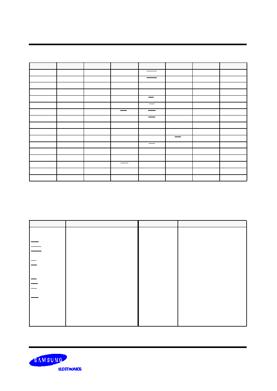
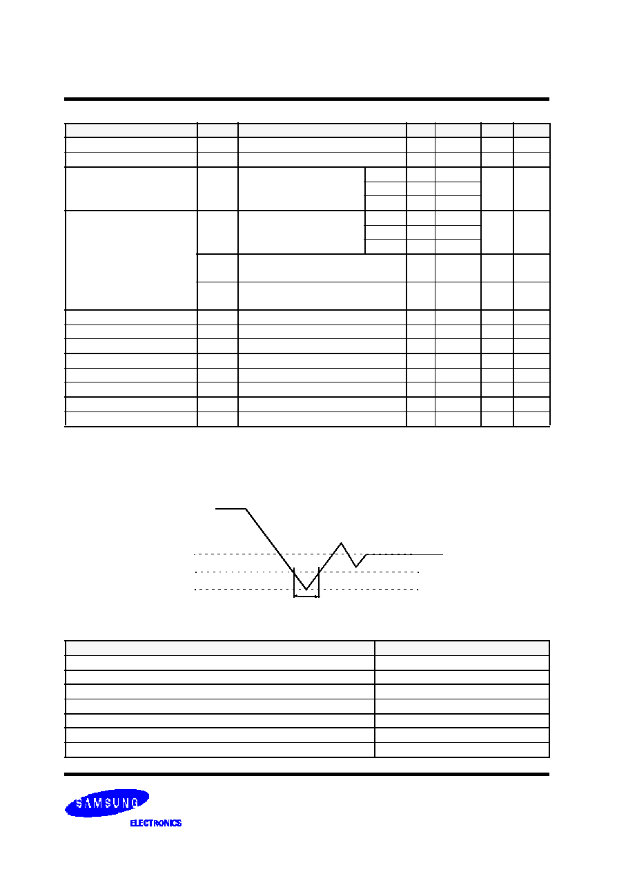
FUNCTION DESCRIPTION
The K7B323625M and K7B321825M are synchronous SRAM designed to support the burst address accessing sequence of the
Power PC based microprocessor. All inputs (with the exception of OE, LBO and ZZ) are sampled on rising clock edges. The start and
duration of the burst access is controlled by ADSC, ADSP and ADV and chip select pins.
The accesses are enabled with the chip select signals and output enabled signals. Wait states are inserted into the access with
ADV.
When ZZ is pulled high, the SRAM will enter a Power Down State. At this time, internal state of the SRAM is preserved. When ZZ
returns to low, the SRAM normally operates after 2cycles of wake up time. ZZ pin is pulled down internally.
Read cycles are initiated with ADSP(or ADSC) using the new external address clocked into the on-chip address register when both
G W and BW are high or when BW is low and WEa, WEb, WEc, and WE d are high. When ADSP is sampled low, the chip selects are
sampled active, and the output buffer is enabled with OE. the data of cell array accessed by the current address are projected to the
output pins.
Write cycles are also initiated with ADSP(or ADSC) and are differentiated into two kinds of operations; All byte write operation and
individual byte write operation.
All byte write occurs by enabling G W(independent of BW and WEx.), and individual byte write is performed only when GW is high
and BW is low. In K7B163625M, a 512Kx36 organization, W Ea controls DQa0 ~ DQa7 and DQPa, WEb controls DQb0 ~ DQb7 and
DQPb, WEc controls DQc0 ~ DQc7 and DQPc and WEd controls DQd0 ~ DQd7 and DQPd.
CS
1
is used to enable the device and conditions internal use of ADSP and is sampled only when a new external address is loaded.
ADV is ignored at the clock edge when ADSP is asserted, but can be sampled on the subsequent clock edges. The address
increases internally for the next access of the burst when ADV is sampled low.
Addresses are generated for the burst access as shown below, The starting point of the burst sequence is provided by the external
address. The burst address counter wraps around to its initial state upon completion. The burst sequence is determined by the state
of the LBO pin. When this pin is Low, linear burst sequence is selected. And this pin is High, Interleaved burst sequence is selected.
BURST SEQUENCE TABLE
(Interleaved Burst)
LBO PIN
HIGH
Case 1
Case 2
Case 3
Case 4
A
1
A
0
A
1
A
0
A
1
A
0
A
1
A
0
First Address
Fourth Address
0
0
1
1
0
1
0
1
0
0
1
1
1
0
1
0
1
1
0
0
0
1
0
1
1
1
0
0
1
0
1
0
BQ TABLE
(Linear Burst)
Note :
1. LBO pin must be tied to High or Low, and Floating State must not be allowed
.
LBO PIN
LOW
Case 1
Case 2
Case 3
Case 4
A
1
A
0
A
1
A
0
A
1
A
0
A
1
A
0
First Address
Fourth Address
0
0
1
1
0
1
0
1
0
1
1
0
1
0
1
0
1
1
0
0
0
1
0
1
1
0
0
1
1
0
1
0
K7B321825M
1Mx36 & 2Mx18 Synchronous SRAM
- 11 -
Rev 1.1
Oct. 2003
K7B323625M
SYNCHRONOUS TRUTH TABLE
Notes :
1. X means "Don
t Care". 2. The rising edge of clock is symbolized by
.
3. WRITE = L means Write operation in WRITE TRUTH TABLE.
WRITE = H means Read operation in WRITE TRUTH TABLE.
4. Operation finally depends on status of asynchronous input pins(ZZ and OE).
CS
1
CS
2
CS
2
ADSP ADSC ADV WRITE
CLK
ADDRESS ACCESSED
OPERATION
H
X
X
X
L
X
X
N/A
Not Selected
L
L
X
L
X
X
X
N/A
Not Selected
L
X
H
L
X
X
X
N/A
Not Selected
L
L
X
X
L
X
X
N/A
Not Selected
L
X
H
X
L
X
X
N/A
Not Selected
L
H
L
L
X
X
X
External Address
Begin Burst Read Cycle
L
H
L
H
L
X
L
External Address
Begin Burst Write Cycle
L
H
L
H
L
X
H
External Address
Begin Burst Read Cycle
X
X
X
H
H
L
H
Next Address
Continue Burst Read Cycle
H
X
X
X
H
L
H
Next Address
Continue Burst Read Cycle
X
X
X
H
H
L
L
Next Address
Continue Burst Write Cycle
H
X
X
X
H
L
L
Next Address
Continue Burst Write Cycle
X
X
X
H
H
H
H
Current Address
Suspend Burst Read Cycle
H
X
X
X
H
H
H
Current Address
Suspend Burst Read Cycle
X
X
X
H
H
H
L
Current Address
Suspend Burst Write Cycle
H
X
X
X
H
H
L
Current Address
Suspend Burst Write Cycle
WRITE TRUTH TABLE
( x36)
Notes :
1. X means "Don
t Care".
2. All inputs in this table must meet setup and hold time around the rising edge of CLK(
).
GW
BW
WEa
WEb
WEc
WE d
OPERATION
H
H
X
X
X
X
READ
H
L
H
H
H
H
READ
H
L
L
H
H
H
WRITE BYTE a
H
L
H
L
H
H
WRITE BYTE b
H
L
H
H
L
L
WRITE BYTE c and d
H
L
L
L
L
L
WRITE ALL BYTEs
L
X
X
X
X
X
WRITE ALL BYTEs
TRUTH TABLES
WRITE TRUTH TABLE
(x18)
Notes :
1. X means "Don
t Care".
2. All inputs in this table must meet setup and hold time around the rising edge of CLK(
).
GW
BW
WEa
WEb
OPERATION
H
H
X
X
READ
H
L
H
H
READ
H
L
L
H
WRITE BYTE a
H
L
H
L
WRITE BYTE b
H
L
L
L
WRITE ALL BYTEs
L
X
X
X
WRITE ALL BYTEs
K7B321825M
1Mx36 & 2Mx18 Synchronous SRAM
- 12 -
Rev 1.1
Oct. 2003
K7B323625M
ABSOLUTE MAXIMUM RATINGS*
*Notes :
Stresses greater than those listed under "Absolute Maximum Ratings" may cause permanent damage to the device. This is a stress rating only
and functional operation of the device at these or any other conditions above those indicated in the operating sections of this specification is not
implied. Exposure to absolute maximum rating conditions for extended periods may affect reliability.
PARAMETER
SYMBOL
RATING
UNIT
Voltage on V
DD
Supply Relative to V
SS
V
DD
-0.3 to 4.6
V
Voltage on V
DDQ
Supply Relative to V
SS
V
DDQ
V
DD
V
Voltage on Input Pin Relative to V
SS
V
IN
-0.3 to V
DD
+0.3
V
Voltage on I/O Pin Relative to V
SS
V
IO
-0.3 to V
DDQ
+0.3
V
Power Dissipation
P
D
1.6
W
Storage Temperature
T
STG
-65 to 150
∞
C
Operating Temperature
T
OPR
0 to 70
∞
C
Storage Temperature Range Under Bias
T
BIAS
-10 to 85
∞
C
CAPACITANCE*
(T
A
=25
∞
C, f=1MHz)
*Note :
Sampled not 100% tested.
PARAMETER
SYMBOL
TEST CONDITION
MIN
MAX
UNIT
Input Capacitance
C
IN
V
IN
=0V
-
5
pF
Output Capacitance
C
OUT
V
OUT
=0V
-
7
pF
ASYNCHRONOUS TRUTH TABLE
Operation
ZZ
OE
I/O STATUS
Sleep Mode
H
X
High-Z
Read
L
L
DQ
L
H
High-Z
Write
L
X
Din, High-Z
Deselected
L
X
High-Z
Notes
1. X means "Don
t Care".
2. ZZ pin is pulled down internally
3. For write cycles that following read cycles, the output buffers must be
disabled with OE, otherwise data bus contention will occur.
4. Sleep Mode means power down state of which stand-by current does
not depend on cycle time.
5. Deselected means power down state of which stand-by current
depends on cycle time.
OPERATING CONDITIONS at 3.3V I/O
(0
∞
C
T
A
70
∞
C)
PARAMETER
SYMBOL
MIN
Typ.
MAX
UNIT
Supply Voltage
V
DD
3.135
3.3
3.465
V
V
DDQ
3.135
3.3
3.465
V
Ground
V
SS
0
0
0
V
OPERATING CONDITIONS at 2.5V I/O
(0
∞
C
T
A
70
∞
C)
PARAMETER
SYMBOL
MIN
Typ.
MAX
UNIT
Supply Voltage
V
DD
3.135
3.3
3.465
V
V
DDQ
2.375
2.5
2.9
V
Ground
V
SS
0
0
0
V
K7B321825M
1Mx36 & 2Mx18 Synchronous SRAM
- 13 -
Rev 1.1
Oct. 2003
K7B323625M
V
SS
V
IH
V
SS-
1.0V
20% t
CYC
(MIN)
(V
DD
=3.3V+0.165V/-0.165V,V
DDQ
=3.3V+0.165/-0.165V or V
DD
=3.3V+0.165V/-0.165V,V
DDQ
=2.5V+0.4V/-0.125V, T
A
=0to70
∞
C)
TEST CONDITIONS
PARAMETER
VALUE
Input Pulse Level(for 3.3V I/O)
0 to 3.0V
Input Pulse Level(for 2.5V I/O)
0 to 2.5V
Input Rise and Fall Time(Measured at 20% to 80% for 3.3V I/O)
1.0V/ns
Input Rise and Fall Time(Measured at 20% to 80% for 2.5V I/O)
1.0V/ns
Input and Output Timing Reference Levels for 3.3V I/O
1.5V
Input and Output Timing Reference Levels for 2.5V I/O
V
DDQ
/2
Output Load
See Fig. 1
DC ELECTRICAL CHARACTERISTICS
(V
DD
=3.3V+0.165V/-0.165V, T
A
=0
∞
C to +70
∞
C)
Notes :
1. Reference AC Operating Conditions and Characteristics for input and timing.
2. Data states are all zero.
3. In Case of I/O Pins, the Max. V
IH
=V
DDQ
+0.3V
Parameter
Symbol
Test Conditions
Min
Max
Unit
Notes
Input Leakage Current(except ZZ)
I
IL
V
DD
=Max ; V
IN
=V
SS
to V
DD
-2
+2
µ
A
Output Leakage Current
I
OL
Output Disabled, V
out
=V
SS
to V
DDQ
-2
+2
µ
A
Operating Current
I
CC
Device Selected, I
OUT
=0mA,
ZZ
V
IL ,
Cycle Time
t
CYC
Min
-65
-
310
mA
1,2
-75
-
290
-85
-
270
Standby Current
I
SB
Device deselected, I
OUT
=0mA,
ZZ
V
IL
, f=Max, All Inputs
0.2V or
V
DD
-0.2V
-65
-
140
mA
-75
-
130
-85
-
130
I
SB1
Device deselected, I
OUT
=0mA, ZZ
0.2V, f=0,
All Inputs=fixed (V
DD
-0.2V or 0.2V)
-
110
mA
I
SB2
Device deselected, I
OUT
=0mA, ZZ
V
DD
-0.2V,
f=Max, All Inputs
V
IL
or
V
IH
-
100
mA
Output Low Voltage(3.3V I/O)
V
OL
I
OL
=8.0mA
-
0.4
V
Output High Voltage(3.3V I/O)
V
OH
I
OH
=-4.0mA
2.4
-
V
Output Low Voltage(2.5V I/O)
V
OL
I
OL
=1.0mA
-
0.4
V
Output High Voltage(2.5V I/O)
V
OH
I
OH
=-1.0mA
2.0
-
V
Input Low Voltage(3.3V I/O)
V
IL
-0.3*
0.8
V
Input High Voltage(3.3V I/O)
V
IH
2.0
V
DD
+0.3**
V
3
Input Low Voltage(2.5V I/O)
V
IL
-0.3*
0.7
V
Input High Voltage(2.5V I/O)
V
IH
1.7
V
DD
+0.3**
V
3

K7B321825M
1Mx36 & 2Mx18 Synchronous SRAM
- 14 -
Rev 1.1
Oct. 2003
K7B323625M
Output Load(B),
(for t
LZC
, t
LZOE
, t
HZOE
& t
HZC
)
Dout
353
/
1538
5pF*
+3.3V for 3.3V I/O
319
/
1667
Fig. 1
* Including Scope and Jig Capacitance
Output Load(A)
Dout
Zo=50
RL=50
VL=1.5V for 3.3V I/O
V
DDQ
/2 for 2.5V I/O
/+2.5V for 2.5V I/O
30pF*
AC TIMING CHARACTERISTICS
(V
DD
=3.3V+0.165V/-0.165V, T
A
=0
∞
C to +70
∞
C)
Notes
: 1. All address inputs must meet the specified setup and hold times for all rising clock edges whenever ADSC and/or ADSP is sampled low and
CS is sampled low. All other synchronous inputs must meet the specified setup and hold times whenever this device is chip selected.
2. Both chip selects must be active whenever ADSC or ADSP is sampled low in order for the this device to remain enabled.
3. ADSC or ADSP must not be asserted for at least 2 Clock after leaving ZZ state.
PARAMETER
SYMBOL
-65
-75
-85
UNIT
MIN
MAX
MIN
MAX
MIN
MAX
Cycle Time
t
CYC
7.5
-
8.5
-
10
-
ns
Clock Access Time
t
CD
-
6.5
-
7.5
-
8.5
ns
Output Enable to Data Valid
t
OE
-
3.5
-
3.5
-
4.0
ns
Clock High to Output Low-Z
t
LZC
2.5
-
2.5
-
2.5
-
ns
Output Hold from Clock High
t
OH
2.5
-
2.5
-
2.5
-
ns
Output Enable Low to Output Low-Z
t
LZOE
0
-
0
-
0
-
ns
Output Enable High to Output High-Z
t
HZOE
-
3.5
-
3.5
-
4.0
ns
Clock High to Output High-Z
t
HZC
-
3.8
-
4.0
-
5.0
ns
Clock High Pulse Width
t
CH
2.2
-
2.5
-
3.0
-
ns
Clock Low Pulse Width
t
CL
2.2
-
2.5
-
3.0
-
ns
Address Setup to Clock High
t
AS
1.5
-
2.0
-
2.0
-
ns
Address Status Setup to Clock High
t
SS
1.5
-
2.0
-
2.0
-
ns
Data Setup to Clock High
t
DS
1.5
-
2.0
-
2.0
-
ns
Write Setup to Clock High (GW , BW , WE
X
)
t
WS
1.5
-
2.0
-
2.0
-
ns
Address Advance Setup to Clock High
t
ADVS
1.5
-
2.0
-
2.0
-
ns
Chip Select Setup to Clock High
t
CSS
1.5
-
2.0
-
2.0
-
ns
Address Hold from Clock High
t
AH
0.5
-
0.5
-
0.5
-
ns
Address Status Hold from Clock High
t
SH
0.5
-
0.5
-
0.5
-
ns
Data Hold from Clock High
t
DH
0.5
-
0.5
-
0.5
-
ns
Write Hold from Clock High (G W, BW, WE
X
)
t
WH
0.5
-
0.5
-
0.5
-
ns
Address Advance Hold from Clock High
t
ADVH
0.5
-
0.5
-
0.5
-
ns
Chip Select Hold from Clock High
t
CSH
0.5
-
0.5
-
0.5
-
ns
ZZ High to Power Down
t
PDS
2
-
2
-
2
-
cycle
ZZ Low to Power Up
t
PUS
2
-
2
-
2
-
cycle
K7B321825M
1Mx36 & 2Mx18 Synchronous SRAM
- 15 -
Rev 1.1
Oct. 2003
K7B323625M
IEEE 1149.1 TEST ACCESS PORT AND BOUNDARY SCAN-JTAG
This part contains an IEEE standard 1149.1 Compatible Test Access Port(TAP). The package pads are monitored by the Serial Scan
circuitry when in test mode. This is to support connectivity testing during manufacturing and system diagnostics. Internal data is not
driven out of the SRAM under JTAG control. In conformance with IEEE 1149.1, the SRAM contains a TAP controller, Instruction Reg-
ister, Bypass Register and ID register. The TAP controller has a standard 16-state machine that resets internally upon power-up,
therefore, TRST signal is not required. It is possible to use this device without utilizing the TAP. To disable the TAP controller without
interfacing with normal operation of the SRAM, TCK must be tied to V
SS
to preclude mid level input. TMS and TDI are designed so an
undriven input will produce a response identical to the application of a logic 1, and may be left unconnected. But they may also be
tied to V
DD
through a resistor. TDO should be left unconnected.
TAP Controller State Diagram
JTAG Block Diagram
SRAM
CORE
BYPASS Reg.
Identification Reg.
Instruction Reg.
Control Signals
TAP Controller
TDO
TDI
TMS
TCK
Test Logic Reset
Run Test Idle
0
1
1
1
1
0
0
0
1
0
1
1
0
0
0
1
0
1
1
1
0
0
0
0
0
0
0
Select DR
Capture DR
Shift DR
Exit1 DR
Pause DR
Exit2 DR
Update DR
Select IR
Capture IR
Shift IR
Exit1 IR
Pause IR
Exit2 IR
Update IR
1
1
1
1
1
JTAG Instruction Coding
NOTE
:
1. Places DQs in Hi-Z in order to sample all input data regardless of other
SRAM inputs. This instruction is not IEEE 1149.1 compliant.
2. Places DQs in Hi-Z in order to sample all input data regardless of other
SRAM inputs.
3. TDI is sampled as an input to the first ID register to allow for the serial shift
of the external TDI data.
4. Bypass register is initiated to V
SS
when BYPASS instruction is invoked. The
Bypass Register also holds serially loaded TDI when exiting the Shift DR
states.
5. SAMPLE instruction dose not places DQs in Hi-Z.
6. This instruction is reserved for future use.
IR2 IR1 IR0
Instruction
TDO Output
Notes
0
0
0 EXTEST
Boundary Scan Register
1
0
0
1 IDCODE
Identification Register
3
0
1
0 SAMPLE-Z
Boundary Scan Register
2
0
1
1 BYPASS
Bypass Register
4
1
0
0 SAMPLE
Boundary Scan Register
5
1
0
1 RESERVED Do Not Use
6
1
1
0 BYPASS
Bypass Register
4
1
1
1 BYPASS
Bypass Register
4
K7B321825M
1Mx36 & 2Mx18 Synchronous SRAM
- 16 -
Rev 1.1
Oct. 2003
K7B323625M
Note
: 1. NC and Vss pins included in the scan exit order are read as "X" ( i.e. don
t care).
BIT
PIN ID(x18)
PIN ID(x36)
40
4B
4B
41
4E
4E
42
4G
4G
43
4A
4A
44
3G
3G
45
3C
3C
46
2B
2B
47
3B
3B
48
3A
3A
49
2C
2C
50
2A
2A
51
1B
1B
52
2D
2D
53
1E
1E
54
2F
2F
55
1G
1G
56
2H
2H
57
1D
1D
58
2E
2E
59
2G
2G
60
1H
1H
61
2K
2K
62
1L
1L
63
2M
2M
64
1N
1N
65
2P
1P
66
1K
1K
67
2L
2L
68
2N
2N
69
1P
2P
70
1T
2T
71
3R
3R
72
2T
1T
73
3L
3L
74
2R
2R
75
3T
3T
76
4N
4N
77
4P
4P
BIT
PIN ID(x18)
PIN ID(x36)
1
4H
4H
2
4T
4T
3
5T
5T
4
6T
6T
5
5L
5L
6
6R
6R
7
5R
5R
8
7R
7R
9
5J
5J
10
7T
7T
11
6P
6P
12
7N
7N
13
6M
6M
14
7L
7L
15
6K
6K
16
7P
7P
17
6N
6N
18
6L
6L
19
7K
7K
20
6H
6H
21
7G
7G
22
6F
6F
23
7E
7E
24
6D
7D
25
7H
7H
26
6G
6G
27
6E
6E
28
7D
6D
29
7B
7B
30
6C
6C
31
6A
6A
32
5C
5C
33
5B
5B
34
5G
5G
35
6B
6B
36
4F
4F
37
4M
4M
38
5A
5A
39
4K
4K
BOUNDARY SCAN EXIT ORDER
ID REGISTER DEFINITION
Part
Revision Number
(31:28)
Part Configuration
(27:18)
Vendor Definition
(17:12)
Samsung JEDEC Code
(11: 1)
Start Bit(0)
1Mx36
0000
01000 00100
XXXXXX
00001001110
1
2Mx18
0000
01001 00011
XXXXXX
00001001110
1
SCAN REGISTER DEFINITION
Part
Instruction Register
Bypass Register
ID Register
Boundary Scan
1Mx36
3 bits
1 bits
32 bits
77 bits
2Mx18
3 bits
1 bits
32 bits
77 bits
SCAN INFORMATION ( 119 BGA )
K7B321825M
1Mx36 & 2Mx18 Synchronous SRAM
- 17 -
Rev 1.1
Oct. 2003
K7B323625M
Note
: 1. NC and Vss pins included in the scan exit order are read as "X" ( i.e. don
t care).
BIT
PIN ID(x18)
PIN ID(x36)
40
6A
6A
41
5B
5B
42
5A
5A
43
4A
4A
44
4B
4B
45
3B
3B
46
3A
3A
47
2A
2A
48
2B
2B
49
1B
1B
50
1A
1A
51
1C
1C
52
1D
1D
53
1E
1E
54
1F
1F
55
1G
1G
56
2D
2D
57
2E
2E
58
2F
2F
59
2G
2G
60
1J
1J
61
1K
1K
62
1L
1L
63
1M
1M
64
1N
2J
65
2K
2K
66
2L
2L
67
2M
2M
68
2J
1N
69
2R
2R
70
1R
1R
71
3P
3P
72
3R
3R
73
4R
4R
74
4P
4P
75
6P
6P
76
6R
6R
BIT
PIN ID(x18)
PIN ID(x36)
1
6N
6N
2
8P
8P
3
8R
8R
4
9R
9R
5
9P
9P
6
10P
10P
7
10R
10R
8
11R
11R
9
11P
11P
10
11H
11H
11
11N
11N
12
11M
11M
13
11L
11L
14
11K
11K
15
11J
11J
16
10M
10M
17
10L
10L
18
10K
10K
19
10J
10J
20
11G
11G
21
11F
11F
22
11E
11E
23
11D
11D
24
11C
10G
25
10F
10F
26
10E
10E
27
10D
10D
28
10G
11C
29
11A
11A
30
11B
11B
31
10A
10A
32
10B
10B
33
9A
9A
34
9B
9B
35
8A
8A
36
8B
8B
37
7A
7A
38
7B
7B
39
6B
6B
BOUNDARY SCAN EXIT ORDER
ID REGISTER DEFINITION
Part
Revision Number
(31:28)
Part Configuration
(27:18)
Vendor Definition
(17:12)
Samsung JEDEC Code
(11: 1)
Start Bit(0)
1Mx36
0000
01000 00100
XXXXXX
00001001110
1
2Mx18
0000
01001 00011
XXXXXX
00001001110
1
SCAN REGISTER DEFINITION
Part
Instruction Register
Bypass Register
ID Register
Boundary Scan
1Mx36
3 bits
1 bits
32 bits
75 bits
2Mx18
3 bits
1 bits
32 bits
75 bits
SCAN INFORMATION (165 FBGA )

K7B321825M
1Mx36 & 2Mx18 Synchronous SRAM
- 18 -
Rev 1.1
Oct. 2003
K7B323625M
JTAG TIMING DIAGRAM
JTAG AC Characteristics
Parameter
Symbol
Min
Max
Unit
Note
TCK Cycle Time
t
CHCH
50
-
ns
TCK High Pulse Width
t
CHCL
20
-
ns
TCK Low Pulse Width
t
CLCH
20
-
ns
TMS Input Setup Time
t
MVCH
5
-
ns
TMS Input Hold Time
t
CHMX
5
-
ns
TDI Input Setup Time
t
DVCH
5
-
ns
TDI Input Hold Time
t
CHDX
5
-
ns
SRAM Input Setup Time
t
SVCH
5
-
ns
SRAM Input Hold Time
t
CHSX
5
-
ns
Clock Low to Output Valid
t
CLQV
0
10
ns
TCK
TMS
TDI
PI
t
CHCH
t
MVCH
t
CHMX
t
CHCL
t
CLCH
t
DVCH
t
CHDX
t
CLQV
TDO
(SRAM)
t
SVCH
t
CHSX
JTAG DC OPERATING CONDITIONS
NOTE
: The input level of SRAM pin is to follow the SRAM DC specification
.
Parameter
Symbol
Min
Typ
Max
Unit
Note
Power Supply Voltage
V
DD
3.135
3.3
3.465
V
Input High Level ( 3.3V I/O / 2.5V I/O )
V
IH
2.0 / 1.7
-
V
DD
+0.3
V
Input Low Level ( 3.3V I/O / 2.5V I/O )
V
IL
-0.3
-
0.8 / 0.7
V
Output High Voltage( 3.3V I/O / 2.5V I/O )
V
OH
2.4 / 2.0
-
-
V
Output Low Voltage( 3.3V I/O / 2.5V I/O )
V
OL
-
-
0.4 / 0.4
V
JTAG AC TEST CONDITIONS
Parameter
Symbol
Min
Unit
Note
Input High/Low Level( 3.3V I/O , 2.5V I/O )
V
IH
/V
IL
3.0/0 , 2.5/0
V
Input Rise/Fall Time( 3.3V I/O , 2.5V I/O )
TR/TF
1.0/1.0 , 1.0/1.0
ns
Input and Output Timing Reference Level
V
DDQ
/2
V
K7B321825M
1Mx36 & 2Mx18 Synchronous SRAM
- 19 -
Rev 1.1
Oct. 2003
K7B323625M
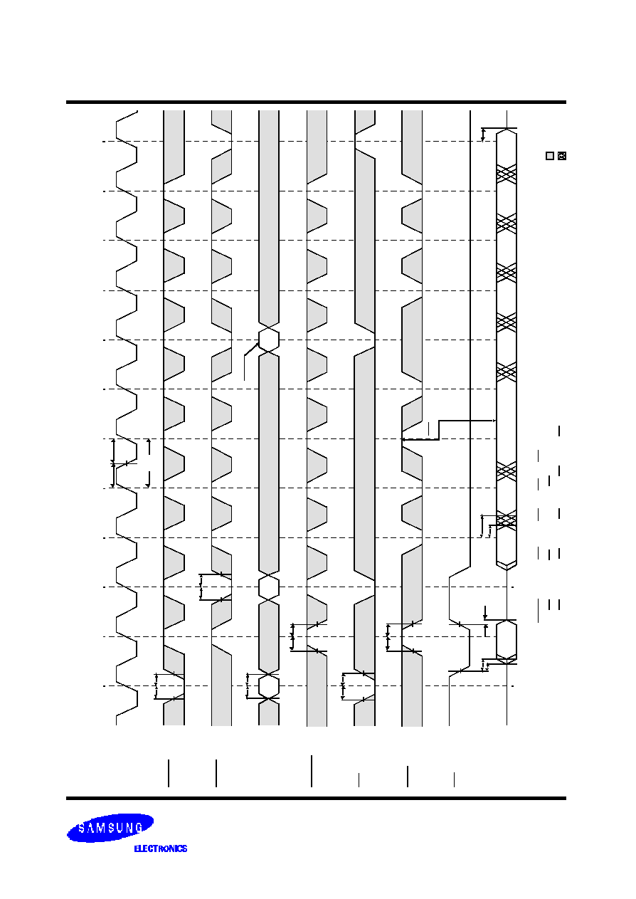
C
L
O
C
K
A
D
S
P
A
D
S
C
A
D
D
R
E
S
S
W
R
I
T
E
C
S
A
D
V
O
E
D
a
t
a
O
u
t
T
I
M
I
N
G
W
A
V
E
F
O
R
M
O
F
R
E
A
D
C
Y
C
L
E
N
O
T
E
S
:
W
R
I
T
E
=
L
m
e
a
n
s
G
W
=
L
,
o
r
G
W
=
H
,
B
W
=
L
,
W
E
x
.
=
L
C
S
=
L
m
e
a
n
s
C
S
1
=
L
,
C
S
2
=
H
a
n
d
C
S
2
=
L
C
S
=
H
m
e
a
n
s
C
S
1
=
H
,
o
r
C
S
1
=
L
a
n
d
C
S
2
=
H
,
o
r
C
S
1
=
L
,
a
n
d
C
S
2
=
L
t
C
H
t
C
L
t
S
S
t
S
H
t
S
S
t
S
H
t
A
S
t
A
H
A
1
A
2
A
3
B
U
R
S
T
C
O
N
T
I
N
U
E
D
W
I
T
H
N
E
W
B
A
S
E
A
D
D
R
E
S
S
t
W
S
t
W
H
t
C
S
S
t
C
S
H
t
A
D
V
S
t
A
D
V
H
t
O
E
t
H
Z
O
E
t
L
Z
O
E
t
C
D
t
O
H
(
A
D
V
I
N
S
E
R
T
S
W
A
I
T
S
T
A
T
E
)
t
H
Z
C
Q
3
-
4
Q
3
-
3
Q
3
-
2
Q
3
-
1
Q
2
-
4
Q
2
-
3
Q
2
-
2
Q
2
-
1
Q
1
-
1
D
o
n
t
C
a
r
e
U
n
d
e
f
i
n
e
d
t
C
Y
C
K7B321825M
1Mx36 & 2Mx18 Synchronous SRAM
- 20 -
Rev 1.1
Oct. 2003
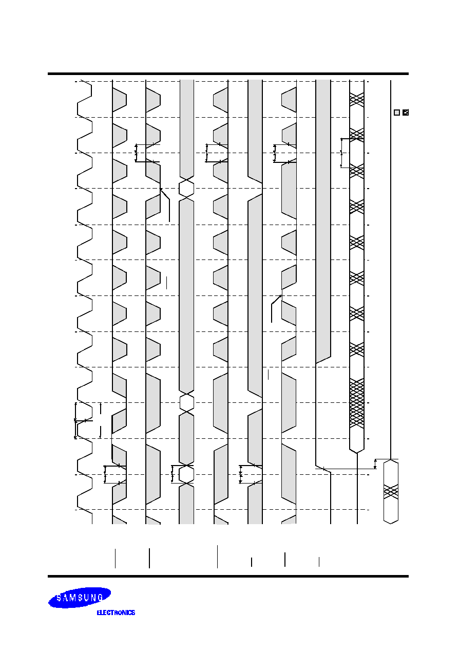
K7B323625M
C
L
O
C
K
A
D
S
P
A
D
S
C
A
D
D
R
E
S
S
W
R
I
T
E
C
S
A
D
V
D
a
t
a
I
n
O
E
D
a
t
a
O
u
t
t
C
H
t
C
L
t
S
S
t
S
H
t
A
S
t
A
H
A
1
A
2
A
3
(
A
D
S
C
E
X
T
E
N
D
E
D
B
U
R
S
T
)
t
L
Z
O
E
D
2
-
1
D
1
-
1
t
C
S
S
t
C
S
H
(
A
D
V
S
U
S
P
E
N
D
S
B
U
R
S
T
)
D
2
-
2
D
2
-
3
D
2
-
4
D
3
-
1
D
3
-
2
D
3
-
3
D
2
-
2
D
3
-
4
Q
0
-
3
Q
0
-
4
t
S
S
t
S
H
t
W
S
t
W
H
t
A
D
V
S
t
A
D
V
H
t
D
S
t
D
H
T
I
M
I
N
G
W
A
V
E
F
O
R
M
O
F
W
R
T
E
C
Y
C
L
E
D
o
n
t
C
a
r
e
U
n
d
e
f
i
n
e
d
t
C
Y
C
K7B321825M
1Mx36 & 2Mx18 Synchronous SRAM
- 21 -
Rev 1.1
Oct. 2003
K7B323625M
T
I
M
I
N
G
W
A
V
E
F
O
R
M
O
F
C
O
M
B
I
N
A
T
I
O
N
R
E
A
D
/
W
R
T
E
C
Y
C
L
E
(
A
D
S
P
C
O
N
T
R
O
L
L
E
D
,
A
D
S
C
=
H
I
G
H
)
C
L
O
C
K
A
D
S
P
A
D
D
R
E
S
S
W
R
I
T
E
C
S
A
D
V
O
E
D
a
t
a
O
u
t
t
C
H
t
C
L
t
D
S
t
D
H
Q
3
-
3
D
a
t
a
I
n
t
O
E
t
O
H
A
1
A
2
A
3
D
2
-
1
Q
3
-
1
Q
3
-
2
Q
3
-
4
t
S
S
t
S
H
t
A
S
t
A
H
t
W
S
t
W
H
t
A
D
V
S
t
A
D
V
H
t
L
Z
O
E
t
H
Z
O
E
t
C
D
t
H
Z
C
t
L
Z
C
D
o
n
t
C
a
r
e
U
n
d
e
f
i
n
e
d
t
C
Y
C
Q
1
-
1
K7B321825M
1Mx36 & 2Mx18 Synchronous SRAM
- 22 -
Rev 1.1
Oct. 2003
K7B323625M
T
I
M
I
N
G
W
A
V
E
F
O
R
M
O
F
S
I
N
G
L
E
R
E
A
D
/
W
R
I
T
E
C
Y
C
L
E
(
A
D
S
C
C
O
N
T
R
O
L
L
E
D
,
A
D
S
P
=
H
I
G
H
)
C
L
O
C
K
A
D
S
C
A
D
D
R
E
S
S
W
R
I
T
E
C
S
A
D
V
O
E
D
a
t
a
I
n
t
C
H
t
C
L
t
H
Z
O
E
D
6
-
1
D
a
t
a
O
u
t
t
W
S
t
W
H
t
C
D
t
O
H
t
O
E
D
5
-
1
D
7
-
1
t
W
S
t
W
H
t
L
Z
O
E
t
D
H
t
D
S
A
1
A
2
A
3
A
4
A
5
A
6
A
7
A
8
A
9
Q
3
-
1
Q
1
-
1
Q
2
-
1
Q
4
-
1
Q
8
-
1
Q
9
-
1
t
C
S
S
t
C
S
H
t
S
S
t
S
H
D
o
n
t
C
a
r
e
U
n
d
e
f
i
n
e
d
t
C
Y
C
K7B321825M
1Mx36 & 2Mx18 Synchronous SRAM
- 23 -
Rev 1.1
Oct. 2003
K7B323625M
D
7
-
1
T
I
M
I
N
G
W
A
V
E
F
O
R
M
O
F
S
I
N
G
L
E
R
E
A
D
/
W
R
I
T
E
C
Y
C
L
E
(
A
D
S
P
C
O
N
T
R
O
L
L
E
D
,
A
D
S
C
=
H
I
G
H
)
C
L
O
C
K
A
D
S
P
A
D
D
R
E
S
S
W
R
I
T
E
C
S
A
D
V
O
E
D
a
t
a
I
n
t
C
H
t
C
L
t
H
Z
O
E
D
a
t
a
O
u
t
t
A
S
t
A
H
t
C
D
t
O
H
t
O
E
D
5
-
1
t
L
Z
O
E
t
D
H
t
D
S
A
1
A
2
A
3
A
4
A
5
A
6
A
9
Q
3
-
1
Q
1
-
1
Q
2
-
1
Q
4
-
1
Q
8
-
1
Q
9
-
1
t
C
S
S
t
C
S
H
t
S
S
t
S
H
A
7
A
8
D
6
-
1
D
o
n
t
C
a
r
e
U
n
d
e
f
i
n
e
d
t
C
Y
C
K7B321825M
1Mx36 & 2Mx18 Synchronous SRAM
- 24 -
Rev 1.1
Oct. 2003
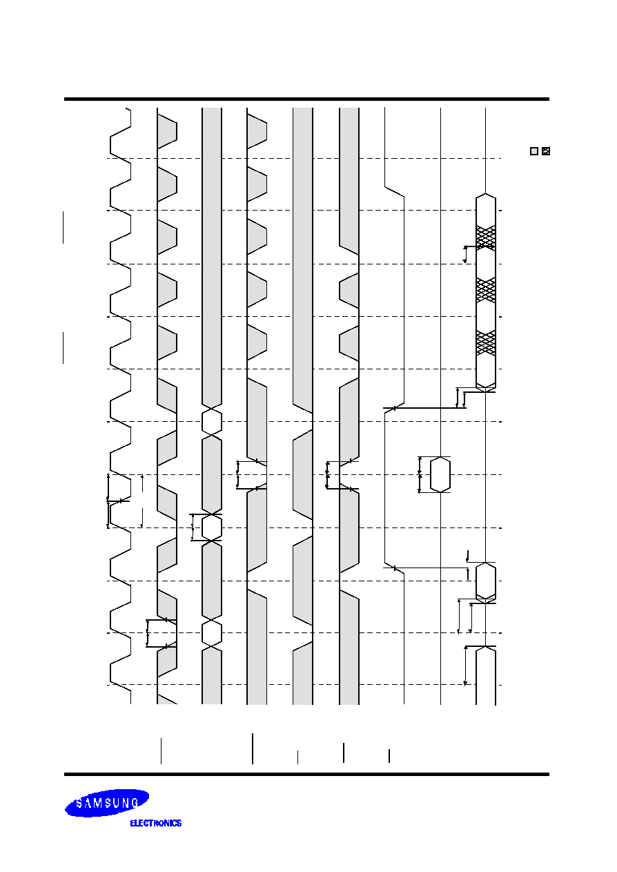
K7B323625M
T
I
M
I
N
G
W
A
V
E
F
O
R
M
O
F
P
O
W
E
R
D
O
W
N
C
Y
C
L
E
C
L
O
C
K
A
D
S
P
A
D
D
R
E
S
S
W
R
I
T
E
C
S
A
D
V
D
a
t
a
I
n
t
C
H
t
C
L
D
2
-
2
O
E
t
W
H
t
H
Z
O
E
t
L
Z
O
E
D
2
-
1
A
1
t
S
S
t
S
H
D
a
t
a
O
u
t
t
P
U
S
A
2
A
D
S
C
Q
1
-
1
Z
Z
t
A
S
t
A
H
t
C
S
S
t
C
S
H
t
O
E
t
H
Z
C
t
P
D
S
S
l
e
e
p
S
t
a
t
e
Z
Z
S
e
t
u
p
C
y
c
l
e
N
o
r
m
a
l
O
p
e
r
a
t
i
o
n
M
o
d
e
Z
Z
R
e
c
o
v
e
r
y
C
y
c
l
e
t
W
S
D
o
n
t
C
a
r
e
U
n
d
e
f
i
n
e
d
t
C
Y
C
K7B321825M
1Mx36 & 2Mx18 Synchronous SRAM
- 25 -
Rev 1.1
Oct. 2003
K7B323625M
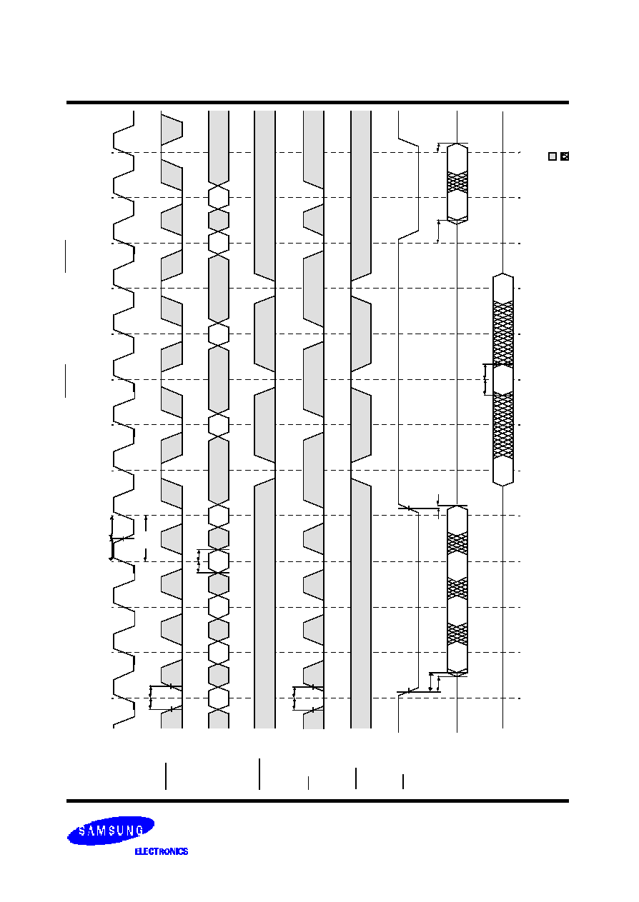
APPLICATION INFORMATION
DEPTH EXPANSION
Data
Address
CLK
ADS
CS
2
CS
2
CLK
ADSC
WEx
OE
CS
1
Address Data
ADV
ADSP
1Mx36
SB
SRAM
(Bank 0)
CS
2
CS
2
CLK
ADSC
WEx
OE
CS
1
Address Data
ADV
ADSP
1Mx36
SB
SRAM
(Bank 1)
CLK
Address
Cache
Controller
A
[0:20]
A
[20]
A
[0:19]
A
[20]
A
[0:19]
I/O
[0:71]
Microprocessor
*Notes :
n = 14 32K depth , 15 64K depth
16 128K depth , 17 256K depth
18 512K depth , 19 1M depth
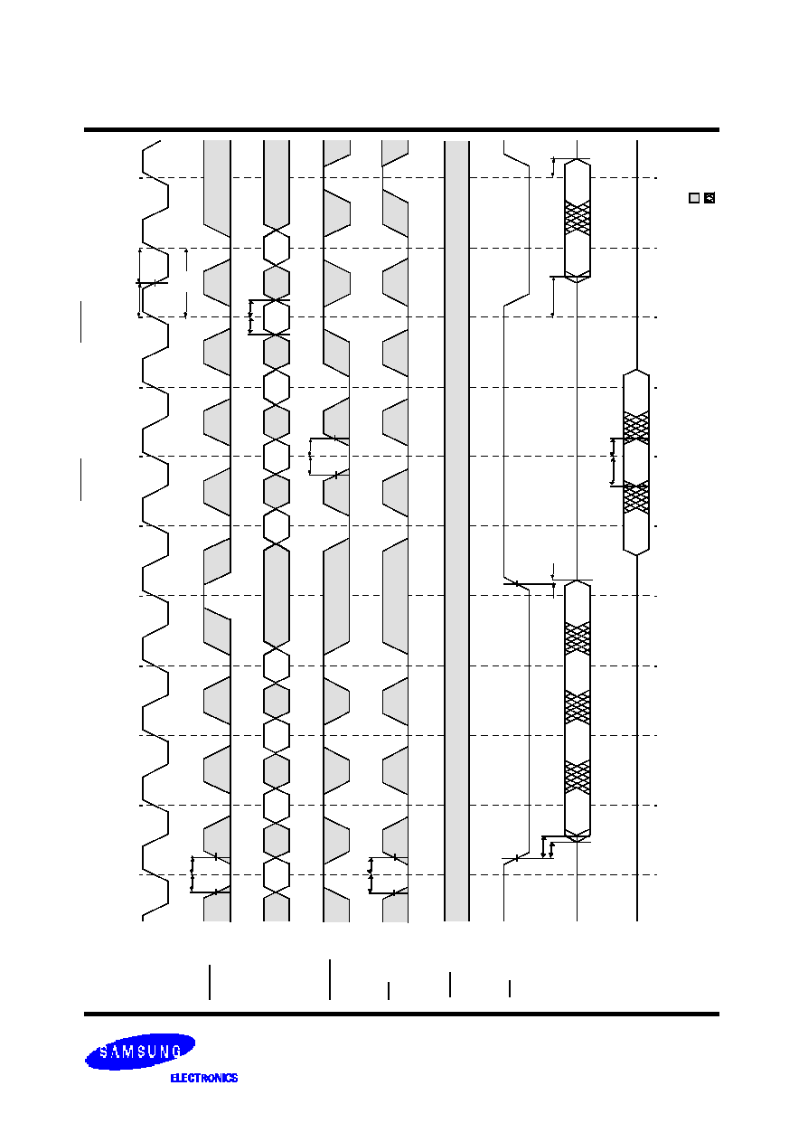
CLOCK
ADSP
ADDRESS
Data Out
INTERLEAVE READ TIMING
(Refer to non-interleave write timing for interleave write timing)
Bank 0 is selected by CS
2
, and Bank 1 deselected by CS
2
Q1-1
Q1-2
Q1-4
Q1-3
OE
Data Out
t
SS
t
SH
A1
A2
WRITE
CS
1
A
n+1
ADV
(Bank 0)
(Bank 1)
Q2-1
Q2-2
Q2-4
Q2-3
t
AS
t
AH
t
CSS
t
CSH
t
WS
t
WH
t
ADVS
t
ADVH
t
OE
t
LZOE
t
HZC
Bank 0 is deselected by CS
2
, and Bank 1 selected by CS
2
[0:n]
Don
t Care
Undefined
t
CD
t
LZC
The Samsung 1Mx36 Synchronous Burst SRAM has two additional chip selects for simple depth expansion.
This permits easy secondary cache upgrades from 1M depth to 2M depth without extra logic.
(ADSP CONTROLLED , ADSC=HIGH)
K7B321825M
1Mx36 & 2Mx18 Synchronous SRAM
- 26 -
Rev 1.1
Oct. 2003
K7B323625M
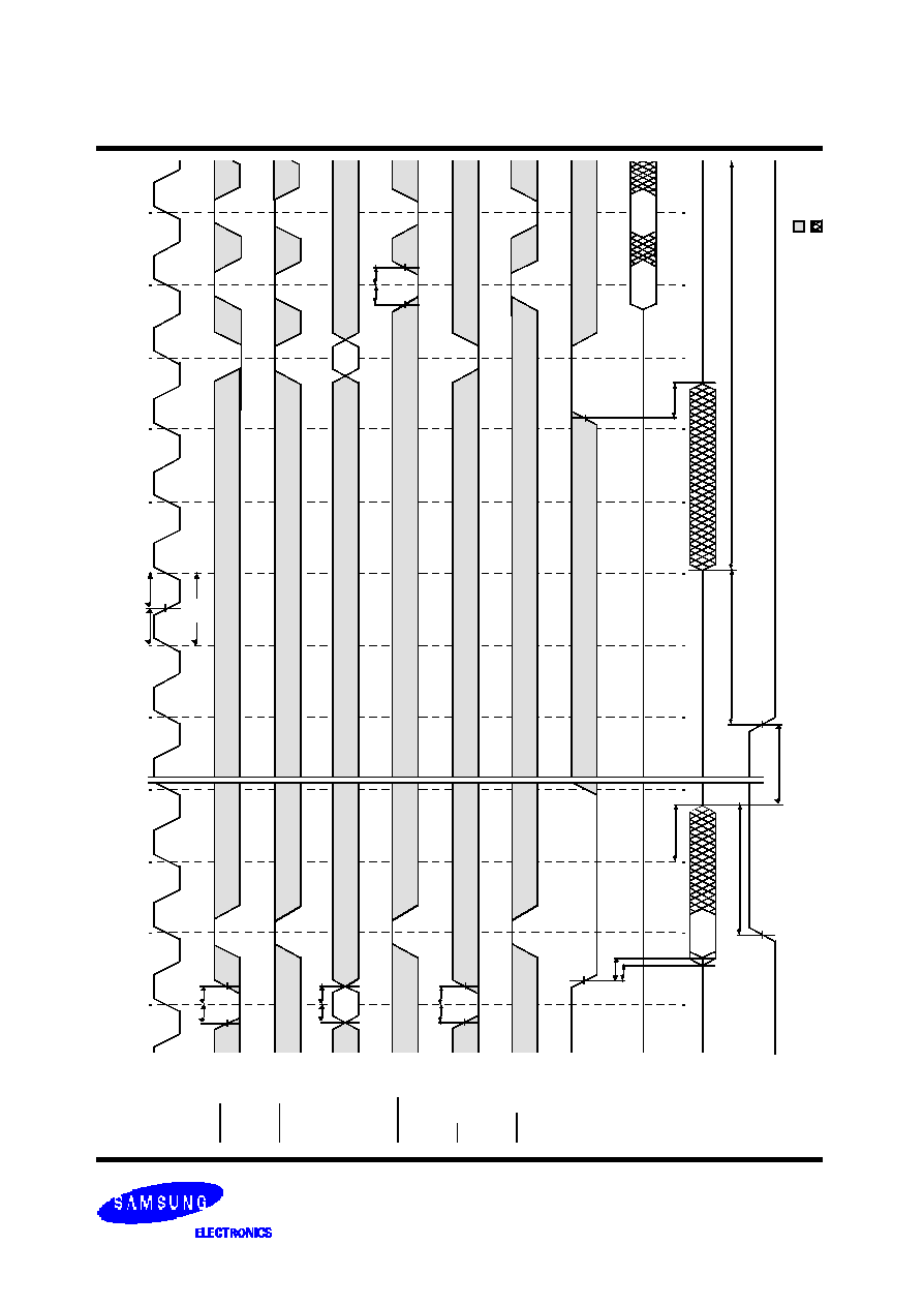
APPLICATION INFORMATION
The Samsung 2Mx18 Synchronous Burst SRAM has two additional chip selects for simple depth expansion.
DEPTH EXPANSION
This permits easy secondary cache upgrades from 2M depth to 4M depth without extra logic.
Data
Address
CLK
ADS
Microprocessor
CS
2
CS
2
CLK
ADSC
WEx
OE
CS
1
Address Data
ADV ADSP
2Mx18
SB
SRAM
(Bank 0)
CS
2
CS
2
CLK
ADSC
WEx
OE
CS
1
Address Data
ADV ADSP
2Mx18
SB
SRAM
(Bank 1)
CLK
Address
Cache
Controller
A
[0:21]
A
[21]
A
[0:20]
A
[21]
A
[0:20]
I/O
[0:71]
CLOCK
ADSP
ADDRESS
Data Out
INTERLEAVE READ TIMING
(Refer to non-interleave write timing for interleave write timing)
Bank 0 is selected by CS
2
, and Bank 1 deselected by CS
2
Q1-1
Q1-2
Q1-4
Q1-3
OE
Data Out
t
SS
t
SH
A1
A2
WRITE
CS
1
A
n+1
ADV
(Bank 0)
(Bank 1)
Q2-1
Q2-2
Q2-4
Q2-3
t
AS
t
AH
t
CSS
t
CSH
t
WS
t
WH
t
ADVS
t
ADVH
t
OE
t
LZOE
t
HZC
Bank 0 is deselected by CS
2
, and Bank 1 selected by CS
2
[0:n]
Don
t Care
Undefined
t
CD
t
LZC
(ADSP CONTROLLED , ADSC=HIGH)
*Notes :
n = 14 32K depth , 15 64K depth
16 128K depth , 17 256K depth
18 512K depth , 19 1M depth
20 2M depth
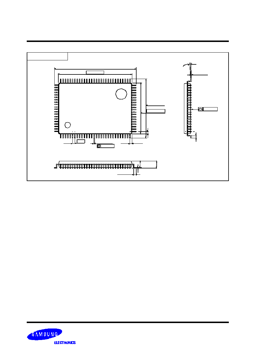
K7B321825M
1Mx36 & 2Mx18 Synchronous SRAM
- 27 -
Rev 1.1
Oct. 2003
K7B323625M
PACKAGE DIMENSIONS
0.10 MAX
0~8
∞
22.00
±
0.30
20.00
±
0.20
16.00
±
0.30
14.00
±
0.20
1.40
±
0.10
1.60 MAX
0.05 MIN
(0.58)
0.50
±
0.10
#1
(0.83)
0.50
±
0.10
100-TQFP-1420A
0.65
0.30
±
0.10
0.10 MAX
+ 0.10
- 0.05
0.127
Units ; millimeters/Inches
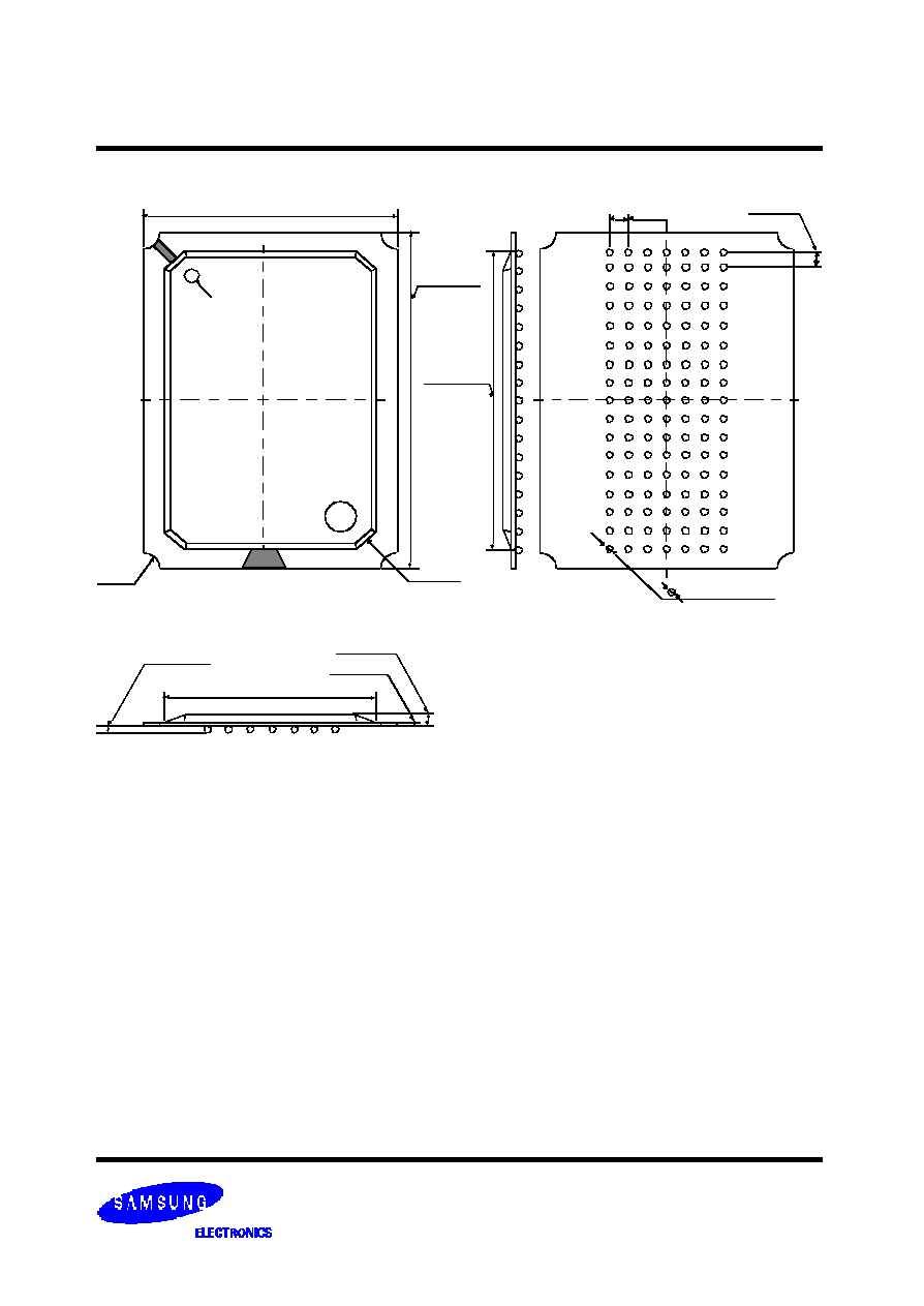
K7B321825M
1Mx36 & 2Mx18 Synchronous SRAM
- 28 -
Rev 1.1
Oct. 2003
K7B323625M
119BGA PACKAGE DIMENSIONS
0.750
±
0.15
1.27
1.27
12.50
±
0.10
0.60
±
0.10
0.60
±
0.10
1.50REF
C1.00
C0.70
14.00
±
0.10
22.00
±
0.10
20.50
±
0.10
NOTE
:
1. All Dimensions are in Millimeters.
2. Solder Ball to PCB Offset : 0.10 MAX.
3. PCB to Cavity Offset : 0.10 MAX.
Indicator of
Ball(1A) Location
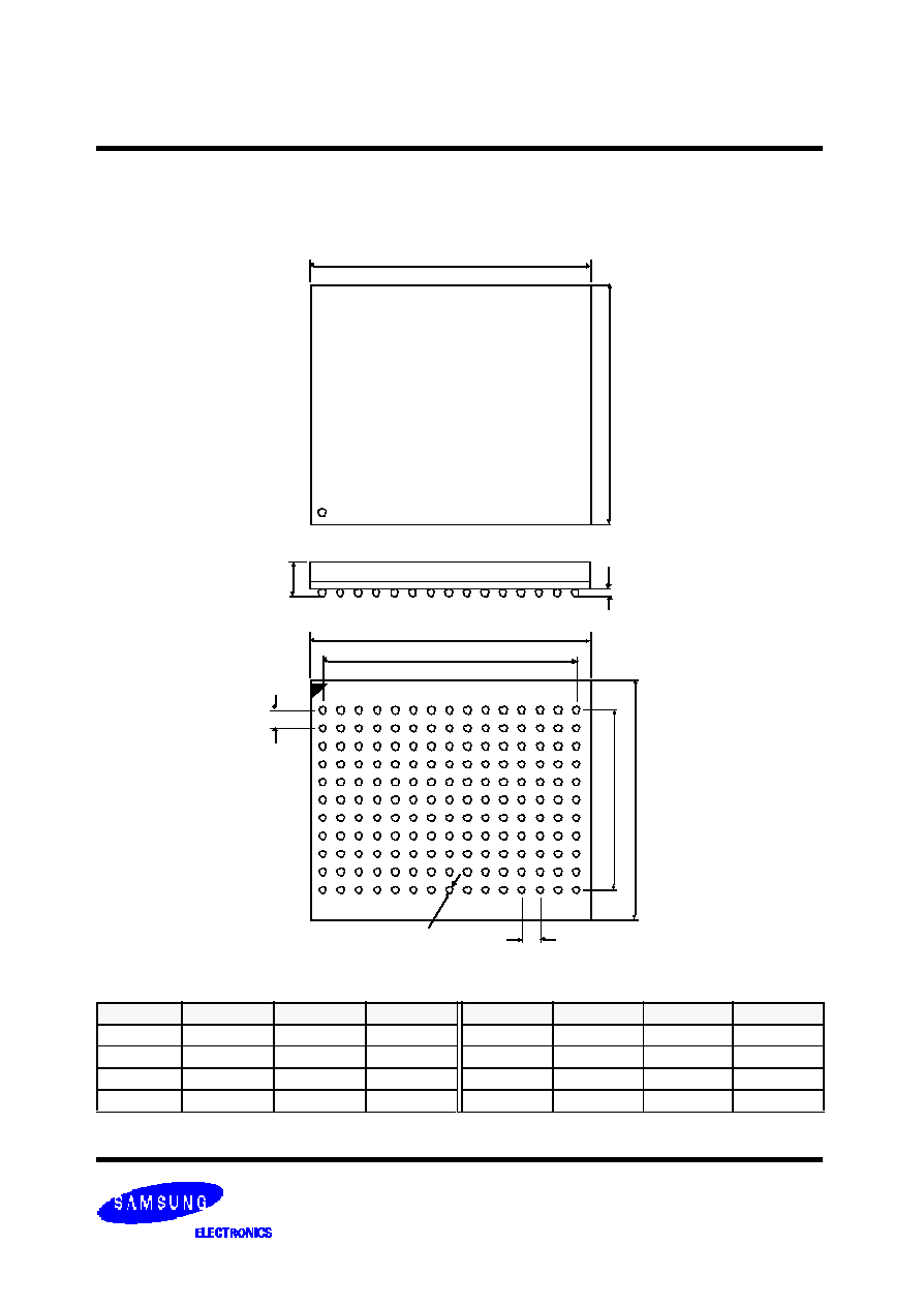
K7B321825M
1Mx36 & 2Mx18 Synchronous SRAM
- 29 -
Rev 1.1
Oct. 2003
K7B323625M
165 FBGA PACKAGE DIMENSIONS
C
Side View
15mm x 17mm Body, 1.0mm Bump Pitch, 11x15 Ball Array
F
A
H
G
B
Bottom View
Top View
A
B
D
E
E
Symbol
Value
Units
Note
Symbol
Value
Units
Note
A
17
±
0.1
mm
E
1.0
mm
B
15
±
0.1
mm
F
14.0
mm
C
1.3
±
0.1
mm
G
10.0
mm
D
0.35
±
0.05
mm
H
0.5
±
0.05
mm