Rev 2.0
512Kx36 & 1Mx18 SRAM
- 1 -
Jan. 2002
K7D161871M
K7D163671M
Document Title
16M DDR SYNCHRONOUS SRAM
Revision History
The attached data sheets are prepared and approved by SAMSUNG Electronics. SAMSUNG Electronics CO., LTD. reserve the
right to change the specifications. SAMSUNG Electronics will evaluate and reply to your requests and questions on the parameters
of this device. If you have any questions, please contact the SAMSUNG branch office near your office, call or cortact Headquarters.
Rev No.
Rev. 0.0
Rev. 0.1
Rev. 0.2
Rev. 0.3
Rev. 0.5
Rev. 0.6
Rev. 0.7
Rev. 1.0
Rev. 2.0
Remark
Advance
Advance
Advance
Advance
Preliminary
Preliminary
Preliminary
Final
Final
History
Initial document.
Addition of New speed bin -25
New part number from KM736FS16017 to K7D163671M
Package height changed.
Leakage current test condition changed from V
DD
to V
DDQ
Package height changed.(From 2.4 to 2.5)
ZQ tolerance changed from 10% to 15%
Deleted -HC25 part(Part Number, Idd, AC Characterisctics)
Add-HC37 part(Part Number, Idd, AC Characteristics)
Clarification on the features and the timing waveforms regarding the
burst controllability.
Package thermal characteristics add
I
DD37
x36 changed from 800mA to 850mA
I
DD37
x18 changed from 750mA to 800mA
Add-HC40 part(Part Number, Idd, AC Characteristics)
Final specification release.
Absolute Maximum Rating VDDQ changed from 3.13V to 2.3V
Draft Data
March. 1999
April. 2000
May. 2000
Aug. 2000
Jan. 2001
April. 2001
May. 2001
Sep. 2001
Jan. 2002
Rev 2.0
512Kx36 & 1Mx18 SRAM
- 2 -
Jan. 2002
K7D161871M
K7D163671M
FEATURES
∑ 512Kx36 or 1Mx18 Organizations.
∑ Maximum Frequency : 400MHz (Data Rate : 800Mbps)
∑ 2.5V V
DD
/1.5V V
DDQ
(1.9V max V
DDQ
).
∑ HSTL Input and Outputs.
∑ Single Differential HSTL Clock.
∑ Synchronous Pipeline Mode of Operation with Self-Timed Late Write.
∑ Free Running Active High and Active Low Echo Clock Output Pin.
∑ Asynchronous Output Enable.
∑ Registered Addresses, Burst Control and Data Inputs.
∑ Registered Outputs.
∑ Single and Double Data Rate Burst Read and Write.
∑ Burst Count Controllable With Max Burst Length of 4
∑ Interleved and Linear Burst mode support
∑ Bypass Operation Support
∑ Programmable Impedance Output Drivers.
NOTE : *Access time equals
t
KXCH/
t
KXCL
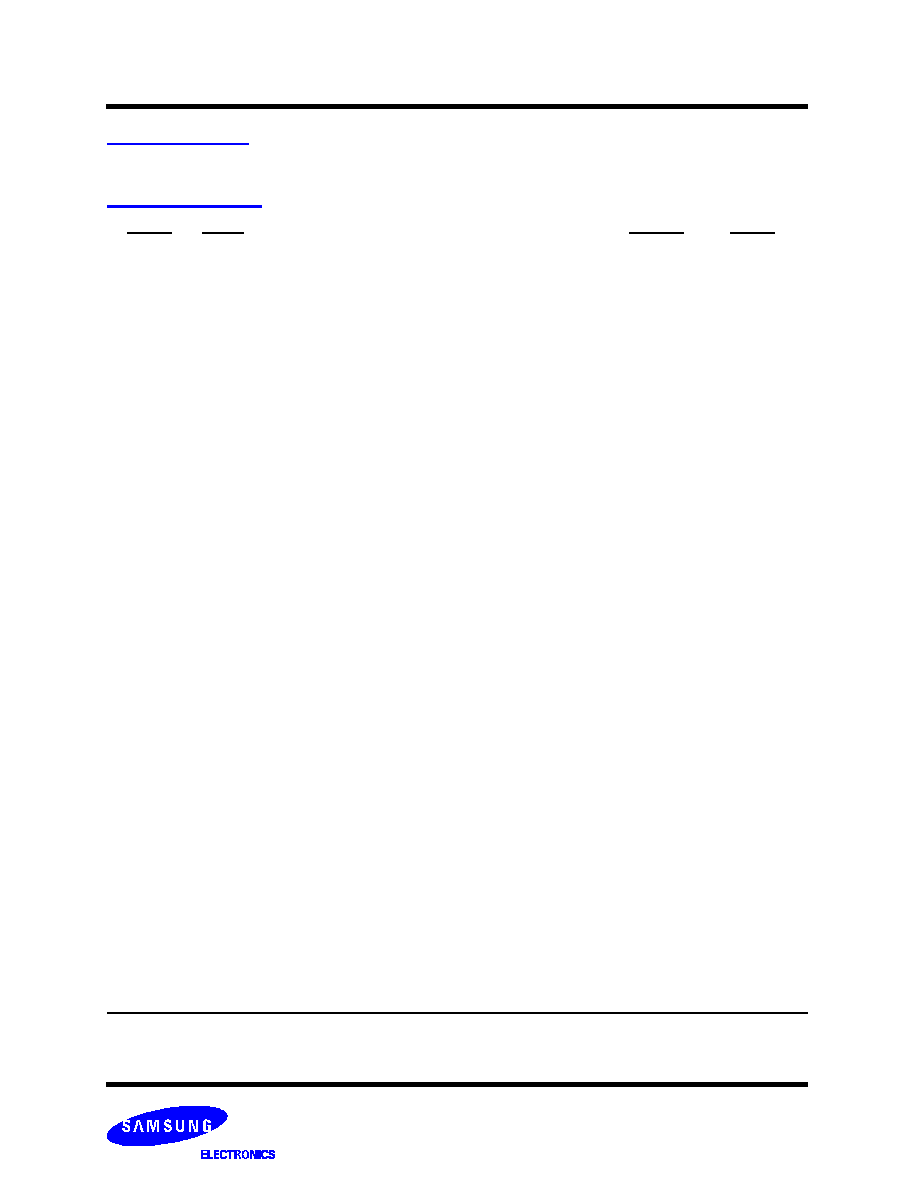
Organization
Part Number
Maximum
Frequency
Access
Time
512Kx36
K7D163671M-HC40
400MHz
1.6*
K7D163671M-HC37
370MHz
1.7*
K7D163671M-HC33
333MHz
1.7*
K7D163671M-HC30
300MHz
1.9*
1Mx18
K7D161871M-HC40
400MHz
1.6*
K7D161871M-HC37
370MHz
1.7*
K7D161871M-HC33
333MHz
1.7*
K7D161871M-HC30
300MHz
1.9*
FUNCTIONAL BLOCK DIAGRAM
K,K
B
1
B
3
B
2
G
Register
CE
Memory Array
512Kx36
Data Out
Data In
Advance
Control
SD/DD
Co
Clock
Synchronous
Buffer
Internal
Clock
Generator
CE
R/W
LD
Data Output Strobe
Data Output Enable
State Machine
Strobe_out
S/A Array
2 : 1 MUX
Data In
Register
Write Buffer
W/D
Array
Echo Clock
Output
36(or 18)x2
36(or 18)x2
36(or18)x2
36(or18)x2
XDIN
CQ,CQ
DQ
36(or 18)
Select
&
R/W control
Output
Buffer
Write
CE
Burst
Counter
Register
Address
Address
Comparator
2:1
MUX
Dec.
19(or 20)
17(or 18)
17(or 18)
19(or 20)
(Burst Write
SA[0:18]( or SA[0:19])
or
(1Mx18)
(2 stage)
(2 stage)
(Burst Address)
Address)
∑ JTAG Boundary Scan (subset of IEEE std. 1149.1)
∑ 153(9x17) Flip Chip Ball Grid Array Package(14mmx22mm)
PIN DESCRIPTION
Pin Name
Pin Description
Pin Name
Pin Description
K, K
Differential Clocks
ZQ
Output Driver Impedance Control Input
SA
Synchronous Address Input
TCK
JTAG Test Clock
SA
0
, SA
1
Synchronous Burst Address Input (SA
0
= LSB)
TMS
JTAG Test Mode Select
DQ
Synchronous Data I/O
TDI
JTAG Test Data Input
CQ, CQ
Differential Output Echo Clocks
TDO
JTAG Test Data Output
B
1
Load External Address
V
REF
HSTL Input Reference Voltage
B
2
Burst R/W Enable
V
DD
Power Supply
B
3
Single/Double Data Selection
V
DDQ
Output Power Supply
G
Asynchronous Output Enable
V
SS
GND
LBO
Linear Burst Order
NC
No Connection
Rev 2.0
512Kx36 & 1Mx18 SRAM
- 3 -
Jan. 2002
K7D161871M
K7D163671M
PACKAGE PIN CONFIGURATIONS
(TOP VIEW)
K7D163671M(512Kx36)
* Mode Pin(6L) is a internally NC.
1
2
3
4
5
6
7
8
9
A
V
SS
V
DDQ
SA
SA
ZQ
SA
SA
V
DDQ
V
SS
B
DQ
C8
DQ
C9
SA
V
SS
B
1
V
SS
SA
DQ
B9
DQ
B8
C
V
SS
V
DDQ
SA
SA
G
SA
SA
V
DDQ
V
SS
D
DQ
C4
DQ
C7
SA
V
SS
V
DD
V
SS
SA
DQ
B7
DQ
B6
E
V
SS
V
DDQ
V
SS
V
DD
V
REF
V
DD
V
SS
V
DDQ
V
SS
F
DQ
C3
CQ
1
DQ
C5
V
DD
V
DD
V
DD
DQ
B5
CQ
2
DQ
B4
G
V
SS
V
DDQ
V
SS
V
SS
K
V
SS
V
SS
V
DDQ
V
SS
H
DQ
C1
DQ
C2
DQ
C6
V
DD
K
V
DD
DQ
B3
DQ
B2
DQ
B1
J
V
SS
V
DDQ
V
SS
V
DD
V
DD
V
DD
V
SS
V
DDQ
V
SS
K
DQ
D1
DQ
D2
DQ
D6
V
SS
B
2
V
SS
DQ
A3
DQ
A2
DQ
A1
L
V
SS
V
DDQ
V
SS
LBO
B
3
MODE
V
SS
V
DDQ
V
SS
M
DQ
D3
CQ
1
DQ
D5
V
DD
V
DD
V
DD
DQ
A5
CQ
2
DQ
A4
N
V
SS
V
DDQ
V
SS
V
DD
V
REF
V
DD
V
SS
V
DDQ
V
SS
P
DQ
D4
DQ
D7
NC
V
SS
V
DD
V
SS
SA
DQ
A7
DQ
A6
R
V
SS
V
DDQ
V
DD
SA
SA
1
SA
V
DD
V
DDQ
V
SS
T
DQ
D8
DQ
D9
SA
V
SS
SA
0
V
SS
SA
DQ
A9
DQ
A8
U
V
SS
V
DDQ
TMS
TDI
TCK
TDO
NC
V
DDQ
V
SS
K7D161871M(1Mx18)
* Mode Pin(6L)is a internally NC.
1
2
3
4
5
6
7
8
9
A
V
SS
V
DDQ
SA
SA
ZQ
SA
SA
V
DDQ
V
SS
B
NC
DQ
B9
SA
V
SS
B
1
V
SS
SA
NC
DQ
A8
C
V
SS
V
DDQ
SA
SA
G
SA
SA
V
DDQ
V
SS
D
DQ
B4
NC
SA
V
SS
V
DD
V
SS
SA
DQ
A7
NC
E
V
SS
V
DDQ
V
SS
V
DD
V
REF
V
DD
V
SS
V
DDQ
V
SS
F
NC
CQ
1
NC
V
DD
V
DD
V
DD
DQ
A5
NC
DQ
A4
G
V
SS
V
DDQ
V
SS
V
SS
K
V
SS
V
SS
V
DDQ
V
SS
H
DQ
B1
NC
DQ
B6
V
DD
K
V
DD
NC
DQ
A2
NC
J
V
SS
V
DDQ
V
SS
V
DD
V
DD
V
DD
V
SS
V
DDQ
V
SS
K
NC
DQ
B2
NC
V
SS
B
2
V
SS
DQ
A3
NC
DQ
A1
L
V
SS
V
DDQ
V
SS
LBO
B
3
MODE
V
SS
V
DDQ
V
SS
M
DQ
B3
NC
DQ
B5
V
DD
V
DD
V
DD
NC
CQ
1
NC
N
V
SS
V
DDQ
V
SS
V
DD
V
REF
V
DD
V
SS
V
DDQ
V
SS
P
NC
DQ
B7
SA
V
SS
V
DD
V
SS
SA
NC
DQ
6
R
V
SS
V
DDQ
V
DD
SA
SA
1
SA
V
DD
V
DDQ
V
SS
T
DQ
B8
NC
SA
V
SS
SA
0
V
SS
SA
DQ
A9
NC
U
V
SS
V
DDQ
TMS
TDI
TCK
TDO
NC
V
DDQ
V
SS

Rev 2.0
512Kx36 & 1Mx18 SRAM
- 4 -
Jan. 2002
K7D161871M
K7D163671M
FUNCTION DESCRIPTION
The K7D163671M and K7D161871M are 18,874,368 bit Synchronous Pipeline Burst Mode SRAM devices. They are organized as
524,288 words by 36 bits for K7D163671M and 1,048,576 words by 18 bits for K7D161871M, fabricated using Samsung's advanced
CMOS technology.
Single differential HSTL level clock, K and K are used to initiate the read/write operation and all internal operations are self-timed. At
the rising edge of K clock, all addresses and burst control inputs are registered internally. Data inputs are registered one cycle after
write addresses are asserted(Late Write), at the rising edge of K clock for single data rate (SDR) write operations and at rising and
falling edge of K clock for a double data rate (DDR) write operations.
Data outputs are updated from output registers off the rising edges of K clock for SDR read operations and off the rising and falling
edges of K clock for DDR read operations. Free running echo clocks are supported which are representive of data output access
time for all SDR and DDR operations.
The chip is operated with a single +2.5V power supply and is compatible with Extended HSTL input and output. The package is
9x17(153) Ball Grid Array balls on a 1.27mm pitch.
Read Operation(Single and Double)
During SDR read operations, addresses and controls are registered at the first rising edge of K clock and then the internal array is
read between first and second rising edges of K clock. Data outputs are updated from output registers off the second rising edge of
K clock. During DDR read operations, addresses and controls are registered at the first rising edge of K clock, and then the internal
array is read twice between first and second rising edges of K clock. Data outputs are updated from output registers sequentially by
burst order off the second rising and falling edge of K clock.
Interleave and linear burst operation is controlled by LBO pin and the burst count is controllable with the maximum burst length of 4.
To avoid data contention,at least one NOP operations are required between the last read and the first write operation.
Write Operation(Late Write)
During SDR write operations, addresses and controls are registered at the first rising edge of K clock and data inputs are registered
at the following rising edge of K clock. During DDR write operations, addresses and controls are registered at the first rising edge of
K clock and data inputs are registered twice at the following rising and falling edge of K clock. Write addresses and data inputs are
stored in the data in registers until the next write operation, and only at the next write opeation are data inputs fully written into SRAM
array.
Echo clock operation
Free running type of Echo clocks are generated from K clock regardless of read, write and NOP operations. They will stop operation
only when K clock is in the stop mode.
Echo clocks are designed to represent data output access time and this allows the echo clocks to be used as reference to capture
data outputs outputs.
Bypass Read Operation
Bypass read operation occurs when the last write operation is followed by a read operation where write and read addresses are
identical. For this case, data outputs are from the data in registers instead of SRAM array.
Programmable Impedance Output Driver
The data output and echo clock driver impedance are adjusted by an external resistor, RQ, connected between ZQ pin and V
SS
, and
are equal to RQ/5. For example, 250
resistor will give an output impedance of 50
. Output driver impedance tolerance is 15% by
test(10% by design) and is periodically readjusted to reflect the changes in supply voltage and temperature. Impedance updates
occur early in cycles that do not activate the outputs, such as deselect cycles. They may also occur in cycles initiated with G high. In
all cases impedance updates are transparent to the user and do not produce access time "push-outs" or other anomalous behavior
in the SRAM. Impedance updates occur no more often than every 32 clock cycles. Clock cycles are counted whether the SRAM is
selected or not and proceed regardless of the type of cycle being executed. Therefore, the user can be assured that after 33 contin-
uous read cycles have occurred, an impedance update will occur the next time G are high at a rising edge of the K clock. There are
no power up requirements for the SRAM. However, to guarantee optimum output driver impedance after power up, the SRAM needs
1024 non-read cycles.
Rev 2.0
512Kx36 & 1Mx18 SRAM
- 5 -
Jan. 2002
K7D161871M
K7D163671M
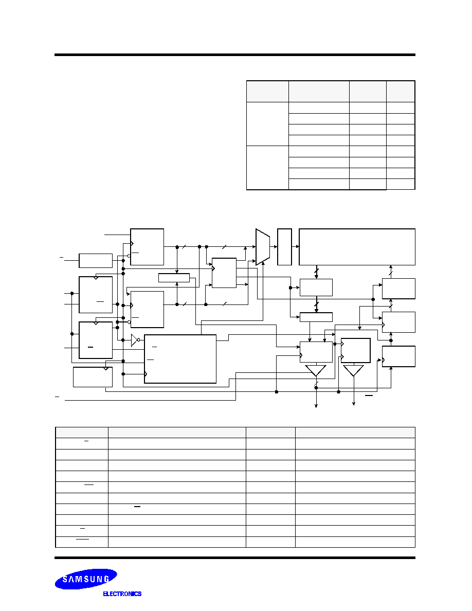
TRUTH TABLE
NOTE : - B(Both) is DIN in write cycle and DOUT in read cycle. Byte write function is not supported. X means "Don't Care".
- K & K are complementary.
K
G
B1
B2
B3
DQ
Operation
L
X
X
X
X
Hi-Z
Clock Stop
X
H
L
X
Hi-Z
No Operation, Pipeline High-Z
L
L
H
H
DOUT
Load Address, Single Read
L
L
H
L
DOUT
Load Address, Double Read
X
L
L
H
DIN
Load Address, Single Write
X
L
L
L
DIN
Load Address, Double Write
X
H
H
X
B
Increment Address, Continue
4 Burst Operation for Interleaved Burst (LBO = V
DDQ
)
NOTE : - For Interleave Burst LBO = V
DDQ
is recommended. If LBO = V
DD
, it must not exceed 2.63V.
Interleaved Burst
Case 1
Case 2
Case 3
Case 4
A
1
A
0
A
1
A
0
A
1
A
0
A
1
A
0
First Address
Fourth Address
0
0
1
1
0
1
0
1
0
0
1
1
1
0
1
0
1
1
0
0
0
1
0
1
1
1
0
0
1
0
1
0
BURST SEQUENCE TABLE
4 Burst Operation for Linear Burst (LBO = V
SS
)
Linear Burst Mode
Case 1
Case 2
Case 3
Case 4
A
1
A
0
A
1
A
0
A
1
A
0
A
1
A
0
First Address
Fourth Address
0
0
1
1
0
1
0
1
0
1
1
0
1
0
1
0
1
1
0
0
0
1
0
1
1
0
0
1
1
0
1
0

Rev 2.0
512Kx36 & 1Mx18 SRAM
- 6 -
Jan. 2002
K7D161871M
K7D163671M
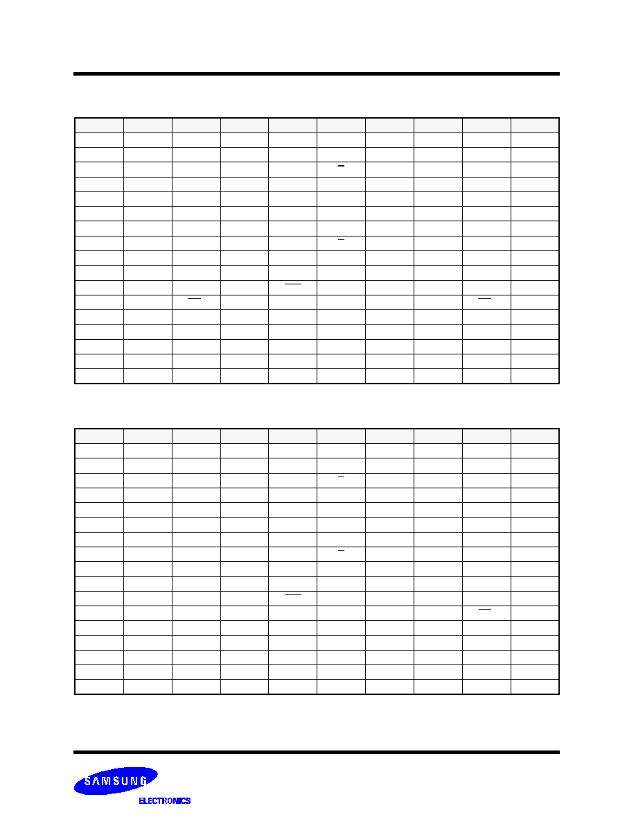
NOTE :
1. State transitions ; B
1
=(Load Address), B
1
=(Increment Address, Continue)
B
2
=(Read), B
2
=(Write)
B
3
=(Single Data Rate), B
3
=(Double Data Rate)
BUS CYCLE STATE DIAGRAM
LOAD
NEW ADDRESS
INCREMENT
ADDRESS
INCREMENT
ADDRESS
INCREMENT
ADDRESS
INCREMENT
ADDRESS
READ
SDR
WRITE
SDR
READ
DDR
WRITE
DDR
B
2
, B
3
B
1
,
B
2
B
1
,
B
2
B
1
,
B
2
B
1
,
B
2
B
1
,
B
2
B
1
,
B
2
B
1
,
B
2
B
1
,
B
2
NO OP
POWER
UP
B
2
, B
3
B
1
B
2
, B
3
B
1
B
2
, B
3
B
1
B
1
B
1
,
B
2
B
1
,
B
2
B
1
,
B
2
B
1
,
B
2
B
1
,
B
2
B
1
,
B
2
B
1
,
B
2
B
1
,
B
2

Rev 2.0
512Kx36 & 1Mx18 SRAM
- 7 -
Jan. 2002
K7D161871M
K7D163671M
RECOMMENDED DC OPERATING CONDITIONS
NOTE :1. These are DC test criteria. DC design criteria is V
REF
±
50mV. The AC V
IH
/V
IL
levels are defined separately for measuring
timing parameters.
2. V
IH
(Max)DC=
V
DDQ
+0.3, V
IH
(Max)AC=
2.6
V (2.1V for DQs) (pulse width
20% of cycle time).
3. V
IL
(Min)DC=
-
0.3V, V
IL
(Min)AC=-1.0V (-0.5V for DQs) (pulse width
20% of cycle time).
Parameter
Symbol
Min
Typ
Max
Unit
Note
Core Power Supply Voltage
V
DD
2.37
2.5
2.63
V
Output Power Supply Voltage
V
DDQ
1.4
1.5
1.9
V
Input High Level Voltage
V
IH
V
REF
+0.1
-
V
DDQ
+0.3
V
1, 2
Input Low Level Voltage
V
IL
-0.3
-
V
REF
-0.1
V
1, 3
Input Reference Voltage
V
REF
0.68
0.75
1.0
V
ABSOLUTE MAXIMUM RATINGS
NOTE : Power Dissipation Capability will be dependent upon package characteristics and use environment. See enclosed thermal impedance data.
Stresses greater than those listed under " Absolute Maximum Ratings" may cause permanent damage to the device. This is a stress rating only
and functional operation of the device at these or any other conditions above those indicated in the operating sections of this specification is not
implied. Exposure to absolute maximum rating conditions for extended periods may affect reliability.
Parameter
Symbol
Value
Unit
Core Supply Voltage Relative to V
SS
V
DD
-0.5 to 3.13
V
Output Supply Voltage Relative to V
SS
V
DDQ
-0.5 to 2.3
V
Voltage on any pin Relative to V
SS
V
IN
-0.5 to V
DDQ
+0.5 (2.3V
MAX
)
V
Output Short-Circuit Current(per I/O)
I
OUT
25
mA
Storage Temperature
T
STR
-55 to 125
∞
C
DC CHARACTERISTICS
NOTE :1. Minimum cycle. I
OUT
=0mA.
2. 50% read cycles.
3. |I
OH
|=(V
DDQ
/2)/(RQ/5)
±
15% @V
OH
=V
DDQ
/2 for 175
RQ
350
.
4. |I
OL
|=(V
DDQ
/2)/(RQ/5)
±
15% @V
OL
=V
DDQ
/2 for 175
RQ
350
.
5. Minimum Impedance Mode when ZQ pin is connected to V
SS
.
Parameter
Symbol
Min
Max
Unit
Note
Average Power Supply Operating Current(x36)
(Cycle time = t
KHKH
min)
I
DD40
I
DD37
I
DD33
I
DD30
-
950
850
750
670
mA
1,2
Average Power Supply Operating Current(x18)
(Cycle time = t
KHKH
min)
I
DD40
I
DD37
I
DD33
I
DD30
-
900
800
700
620
mA
1,2
Stop Clock Standby Current
(V
IN
=V
DD
-0.2V or 0.2V fixed, K=Low, K=High)
I
SB1
-
150
mA
1
Input Leakage Current
(V
IN
=V
SS
or V
DDQ
)
I
LI
-1
1
µ
A
Output Leakage Current
(V
OUT
=V
SS
or V
DDQ
)
I
LO
-1
1
µ
A
Output High Voltage(Programmable Impedance Mode)
V
OH1
V
DDQ
/2
V
DDQ
V
3
Output Low Voltage(Programmable Impedance Mode)
V
OL1
V
SS
V
DDQ
/2
V
4
Output High Voltage(I
OH
=-0.1mA)
V
OH2
V
DDQ
-0.2
V
DDQ
V
5
Output Low Voltage(I
OL
=0.1mA)
V
OL2
V
SS
0.2
V
5
Rev 2.0
512Kx36 & 1Mx18 SRAM
- 8 -
Jan. 2002
K7D161871M
K7D163671M
PIN CAPACITANCE
NOTE : Periodically sampled and not 100% tested.(T
A
=25
∞
C, f=1MHz)
Parameter
Symbol
Test Condition
Min
Max
Unit
Input Capacitance
C
IN
V
IN
=0V
-
4
pF
Data Output Capacitance
C
OUT
V
OUT
=0V
-
5
pF
AC TEST CONDITIONS
(T
A
=0 to 70
∞
C, V
DD
=2.37 -2.63V, V
DDQ
=1.5V)
Parameter
Symbol
Value
Unit
Note
Input High/Low Level
V
IH
/V
IL
1.25/0.25
V
-
Input Reference Level
V
REF
0.75
V
-
Input Rise/Fall Time
T
R
/T
F
0.5/0.5
ns
-
Output Timing Reference Level
0.75
V
-
Clock Input Timing Reference Level
Cross Point
V
-
Output Load
See Below
-
AC CHARACTERISTICS
(T
A
=0 to 70
∞
C, V
DD
=2.37 -2.63V, V
DDQ
=1.5V)
NOTE :
1. See AC Test Output Load figure
2. Design target is 0ns
Parameter
Symbol
-40
-37
-33
-30
Unit
Note
Min
Max
Min
Max
Min
Max
Min
Max
Clock Cycle Time
t
KHKH
2.5
-
2.7
-
3.0
-
3.3
-
ns
Clock High Pulse Width
t
KHKL
1.1
-
1.3
-
1.3
-
1.5
-
ns
Clock Low Pulse Width
t
KLKH
1.1
-
1.3
-
1.3
-
1.5
-
ns
CQ High Pulse Width
t
CHCL
t
KHKL
-0.1 t
KHKL
+0.1 t
KHKL
-0.1 t
KHKL
+0.1 t
KHKL
-0.1 t
KHKL
+0.1 t
KHKL
-0.2 t
KHKL
+0.2
ns
CQ Low Pulse Width
t
CLCH
t
KLKH
-0.1 t
KLKH
+0.1 t
KLKH
-0.1 t
KLKH
+0.1 t
KLKH
-0.1 t
KLKH
+0.1 t
KLKH
-0.2 t
KLKH
+0.2
ns
Clock to Echo Clock(CQ) High
t
KXCH
0.5
1.6
0.5
1.7
0.5
1.7
0.5
1.9
ns
1
Clock to Echo Clock(CQ) Low
t
KXCL
0.5
1.6
0.5
1.7
0.5
1.7
0.5
1.9
ns
Echo Clock to Output Valid
t
CHQV/
t
CLQV
-
0.1
-
0.1
-
0.1
-
0.1
ns
1,2
Echo Clock to Output Hold
t
CHQX/
t
CLQX
-0.15
-
-0.2
-
-0.25
-
-0.3
-
ns
1
Echo Clock to Output High-Z
t
CHQZ/
t
CHLZ
0.1
0.1
0.1
0.1
ns
1
G Low to Output Low-Z
t
GLQX
0.5
-
0.5
-
0.5
-
0.5
-
ns
1
G High to Output High-Z
t
GHQZ
-
1.6
-
1.7
-
1.7
-
1.9
ns
1
G Low to Output Valid
t
GLQV
-
1.6
-
1.7
-
1.7
-
1.9
ns
1
Address Setup Time
t
AVKH
0.4
-
0.4
-
0.4
-
0.4
-
ns
Address Hold Time
t
KHAX
0.4
-
0.4
-
0.4
-
0.4
-
ns
Burst Control Setup Time
t
BVKH
0.4
-
0.4
-
0.4
-
0.4
-
ns
Burst Control Hold Time
t
KHBX
0.3
-
0.3
-
0.3
-
0.3
-
ns
Data Setup Time
t
DVKH
0.25
-
0.25
-
0.25
-
0.3
-
ns
Data Hold Time
t
KHDX
0.25
-
0.25
-
0.25
-
0.3
-
ns
50
50
AC TEST OUTPUT LOAD
25
5pF
DQ
0.75V
5pF
0.75V
50
50
0.75V
Rev 2.0
512Kx36 & 1Mx18 SRAM
- 9 -
Jan. 2002
K7D161871M
K7D163671M
NOP
CONTINUE
K
K
B1
G
SA
t
AVKH
t
KHAX
CQ
NOP
1
2
3
4
5
6
7
8
10
12
11
B2
B3
CQ
DQ
READ
(burst of 4)
READ
(burst of 2)
READ
(burst of 4)
NOP
WRITE
CONTINUE
WRITE
(burst of 4)
READ
9
CONTINUE
READ
READ
(burst of 4)
CONTINUE
READ
A
0
A
1
A
2
A
3
Q
X2
Q
01
Q
02
Q
03
Q
04
Q
51
Q
52
Q
53
Q
54
Q
11
Q
12
D
21
D
23
D
24
D
22
Q
31
t
BVKH
t
KHBX
t
CHQZ
t
KXCH
t
CHLZ
t
CHQV
t
CHQX
t
GHQZ
t
DVKH
t
KHDX
t
GLQX
t
GLQV
t
KHKH
t
GHQX
UNDEFINED
DON'T CARE
A
5
NOTE
1. Q
01
refers to output from address A. Q
02
refers to output from the next internal burst address following A, etc.
2. Outputs are disabled(High-Z) one clock cycle after NOP detected or after no pending data requests are present.
3. Doing more than one Read Continue or Write Continue will cause the address to wrap around.
TIMING WAVEFORMS FOR DOUBLE DATA RATE CYCLES
(Burst Length=4, 2)
Rev 2.0
512Kx36 & 1Mx18 SRAM
- 10
Jan. 2002
K7D161871M
K7D163671M
TIMING WAVEFORMS FOR SINGLE DATA RATE CYCLES
NOTE :
1. Q
01
refers to output from address A
0
. Q
02
refers to output from the next internal burst address following A
0
, etc.
2. Outputs are disabled(High-Z) one clock cycle after NOP detected or after no pending data requests are present.
3. This devices supports cycle lengths of 1, 2, 4. Continue(B1=HIGH, B2=HIGH, B3=X) up to three times following a B1 operation. Any further
Continue assertions constitute invalid operations.
4. This device will have an address wraparound if further Continues are applied.
NOP
CONTINUE
t
KHKH
t
AVKH
t
KHAX
NOP
1
2
3
4
5
6
7
8
10
12
11
READ
(burst of 2)
READ
READ
(burst of 4)
NOP
WRITE
CONTINUE
WRITE
(burst of 2)
READ
9
CONTINUE
READ
CONTINUE
READ
CONTINUE
READ
A
0
A
1
A
2
A
3
Q
X1
D
22
D
21
t
BVKH
t
KHBX
t
CHQZ
t
KXCH
t
CHLZ
t
CHQV
t
CHQX
t
GHQZ
t
GHQX
t
DVKH
t
KHDX
t
GLQX
t
GLQV
t
KLKH
Q
31
Q
01
Q
02
Q
03
Q
04
Q
11
UNDEFINED
DON'T CARE
t
KHKL
K
K
B1
G
SA
B2
B3
DQ
CQ
CQ
(Burst Length=4, 2, 1)
(burst of 1)

Rev 2.0
512Kx36 & 1Mx18 SRAM
- 11
Jan. 2002
K7D161871M
K7D163671M
IEEE 1149.1 TEST ACCESS PORT AND BOUNDARY SCAN-JTAG
TAP Controller State Diagram
JTAG Block Diagram
SRAM
CORE
BYPASS Reg.
Identification Reg.
Instruction Reg.
Control Signals
TAP Controller
TDO
SA
SA
TDI
TMS
TCK
Test Logic Reset
Run Test Idle
0
1
1
1
1
0
0
0
1
0
1
1
0
0
0
1
0
1
1
1
0
0
0
0
0
0
0
Select DR
Capture DR
Shift DR
Exit1 DR
Pause DR
Exit2 DR
Update DR
Select IR
Capture IR
Shift IR
Exit1 IR
Pause IR
Exit2 IR
Update IR
1
1
1
1
1
JTAG Instruction Coding
NOTE :
1. Places DQs in Hi-Z in order to sample all input data regardless of other
SRAM inputs.
2. TDI is sampled as an input to the first ID register to allow for the serial
shift of the external TDI data.
3. Bypass register is initiated to V
SS
when BYPASS instruction is
invoked.
The Bypass Register also holds serially loaded TDI when exiting
the Shift DR states.
4. SAMPLE instruction dose not places DQs in Hi-Z.
IR2 IR1 IR0 Instruction
TDO Output
Notes
0
0
0
EXTEST
Boundary Scan Register
1
0
0
1
IDCODE
Identification Register
2
0
1
0
SAMPLE-Z Boundary Scan Register
1
0
1
1
BYPASS
Bypass Register
3
1
0
0
SAMPLE
Boundary Scan Register
4
1
0
1
BYPASS
Bypass Register
3
1
1
0
BYPASS
Bypass Register
3
1
1
1
BYPASS
Bypass Register
3
The SRAM provides a limited set of IEEE standard 1149.1 JTAG functions. This is to test the connectivity during manufacturing
between SRAM, printed circuit board and other components. Internal data is not driven out of SRAM under JTAG control. In conform-
ance with IEEE 1149.1, the SRAM contains a TAP controller, Instruction Register, Bypass Register and ID register. The TAP control-
ler has a standard 16-state machine that resets internally upon power-up, therefore, TRST signal is not required. It is possible to use
this device without utilizing the TAP. To disable the TAP controller without interfacing with normal operation of the SRAM. TCK must
be tied to V
SS
to preclude mid level input. TMS and TDI are designed so an undriven input will produce a response identical to the
application of a logic 1, and may be left unconnected. But they may also be tied to V
DD
through a resistor. TDO should be left uncon-
nected.

Rev 2.0
512Kx36 & 1Mx18 SRAM
- 12
Jan. 2002
K7D161871M
K7D163671M
BOUNDARY SCAN EXIT ORDER(x36)
* Reserved for Mode Pin
36
4A
SA
SA
6A
35
37
4C
SA
SA
6C
34
38
3A
SA
SA
7A
33
39
3B
SA
SA
7B
32
40
3C
SA
SA
7C
31
41
3D
SA
SA
7D
30
42
2B
DQ
DQ
8B
29
43
1B
DQ
DQ
9B
28
44
2D
DQ
DQ
8D
27
45
3F
DQ
DQ
7F
26
46
1D
DQ
DQ
9D
25
47
2F
CQ
CQ
8F
24
48
1F
DQ
DQ
9F
23
49
3H
DQ
DQ
7H
22
50
2H
DQ
DQ
8H
21
51
1H
DQ
DQ
9H
20
52
5A
ZQ
G
5C
19
53
5B
B
1
K
5G
18
54
5K
B
2
K
5H
17
55
5L
B
3
MODE
6L
16
56
4L
LBO
DQ
9K
15
57
1K
DQ
DQ
8K
14
58
2K
DQ
DQ
7K
13
59
3K
DQ
DQ
9M
12
60
1M
DQ
CQ
8M
11
61
2M
CQ
DQ
9P
10
62
1P
DQ
DQ
7M
9
63
3M
DQ
DQ
8P
8
64
2P
DQ
DQ
9T
7
65
1T
DQ
DQ
8T
6
66
2T
DQ
SA
7P
5
67
3T
SA
SA
7T
4
68
4R
SA
SA
6R
3
SA
5T
2
SA
5R
1
BOUNDARY SCAN EXIT ORDER(x18)
* Reserved for Mode Pin
26
4A
SA
SA
6A
25
27
4C
SA
SA
6C
24
28
3A
SA
SA
7A
23
29
3B
SA
SA
7B
22
30
3C
SA
SA
7C
21
31
3D
SA
SA
7D
20
32
2B
DQ
DQ
9B
19
DQ
8D
18
DQ
7F
17
33
1D
DQ
34
2F
CQ
DQ
9F
16
35
3H
DQ
DQ
8H
15
36
1H
DQ
37
5A
ZQ
G
5C
14
38
5B
B
1
K
5G
13
39
5K
B
2
K
5H
12
40
5L
B
3
MODE
6L
11
41
4L
LBO
DQ
9K
10
42
2K
DQ
DQ
7K
9
43
1M
DQ
CQ
8M
8
DQ
9P
7
44
3M
DQ
45
2P
DQ
46
1T
DQ
DQ
8T
6
SA
7P
5
47
3P
SA
SA
7T
4
48
3T
SA
SA
6R
3
49
4R
SA
SA
5T
2
SA
5R
1
ID REGISTER DEFINITION
Part
Revision Number
(31:28)
Part Configuration
(27:18)
Vendor Definition
(17:12)
Samsung JEDEC Code
(11: 1)
Start Bit
(0)
512Kx36
0000
00111 00100
XXXXXX
00001001110
1
1M x 18
0000
01000 00011
XXXXXX
00001001110
1
SCAN REGISTER DEFINITION
Part
Instruction Register
Bypass Register
ID Register
Boundary Scan
512Kx36
3 bits
1 bits
32 bits
68 bits
1M x 18
3 bits
1 bits
32 bits
49 bits
Rev 2.0
512Kx36 & 1Mx18 SRAM
- 13
Jan. 2002
K7D161871M
K7D163671M
JTAG DC OPERATING CONDITIONS
NOTE : 1. The input level of SRAM pin is to follow the SRAM DC specification.
Parameter
Symbol
Min
Typ
Max
Unit
Note
Power Supply Voltage
V
DD
2.37
2.5
2.63
V
Input High Level
V
IH
1.7
-
V
DD
+0.3
V
Input Low Level
V
IL
-0.3
-
0.7
V
Output High Voltage(I
OH
=-2mA)
V
OH
2.1
-
V
DD
V
Output Low Voltage(I
OL
=2mA)
V
OL
V
SS
-
0.2
V
JTAG AC Characteristics
Parameter
Symbol
Min
Max
Unit
Note
TCK Cycle Time
t
CHCH
50
-
ns
TCK High Pulse Width
t
CHCL
20
-
ns
TCK Low Pulse Width
t
CLCH
20
-
ns
TMS Input Setup Time
t
MVCH
5
-
ns
TMS Input Hold Time
t
CHMX
5
-
ns
TDI Input Setup Time
t
DVCH
5
-
ns
TDI Input Hold Time
t
CHDX
5
-
ns
Clock Low to Output Valid
t
CLQV
0
10
ns
JTAG AC TEST CONDITIONS
NOTE : 1. See SRAM AC test output load on page 5.
Parameter
Symbol
Min
Unit
Note
Input High/Low Level
V
IH
/V
IL
2.5/0.0
V
Input Rise/Fall Time
TR/TF
1.0/1.0
ns
Input and Output Timing Reference Level
1.25
V
1
JTAG TIMING DIAGRAM
TCK
TMS
TDI
TDO
t
CHCH
t
CHCL
t
CLCH
t
MVCH
t
CHMX
t
DVCH
t
CHDX
t
CLQV
Rev 2.0
512Kx36 & 1Mx18 SRAM
- 14
Jan. 2002
K7D161871M
K7D163671M
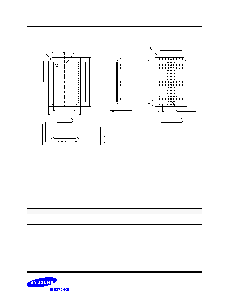
PACKAGE DIMENSIONS
153-FCBGA-1422
Units:millimeters/Inches
7 6 5 4 3 2 1
1
.
2
7
0
BOTTOM VIEW
0.300 MAX M
153-
0.750
±
0.150
14.000
2
2
.
0
0
0
1.27x8=10.160
C
H
I
P
A
R
E
A
TOP VIEW
0.200 MAX
9 8
1
.
2
7
x
1
6
=
2
0
.
3
2
0
1.270
B
C
D
E
F
G
H
J
K
L
M
N
P
R
T
U
A
CHIP AREA
9
.
7
5
0
5.750
R1.250
#A1 INDEX
CHIP BACK SIDE
0
.
6
0
0
2
.
5
0
0
0
.
6
0
0
±
0
.
0
5
0
1
.
2
0
0
±
0
.
1
0
0
UNDERFILL
153 BGA PACKAGE THERMAL CHARACTERISTICS
NOTE : 1. Junction temperature can be calculated by : T
J
= T
A
+ P
D
x Theta_JA.
Parameter
Symbol
Thermal Resistance
Unit
Note
Junction to Ambient(at still air)
Theta_JA
22.8
∞
C/W
1W Heating
Junction to Case
Theta_JC
0.6
∞
C/W
Junction to Board
Theta_JB
4.2
∞
C/W
2W Heating