Äîêóìåíòàöèÿ è îïèñàíèÿ www.docs.chipfind.ru

1Mx36 & 2Mx18 Flow-Through NtRAM
TM
- 1 -
Rev 2.0
Nov. 2003
K7M321825M
K7M323625M
Document Title
1Mx36 & 2Mx18-Bit Flow Through NtRAM
TM
The attached data sheets are prepared and approved by SAMSUNG Electronics. SAMSUNG Electronics CO., LTD. reserve the right to change the
specifications. SAMSUNG Electronics will evaluate and reply to your requests and questions on the parameters of this device. If you have any ques-
tions, please contact the SAMSUNG branch office near your office, call or contact Headquarters.
Revision History
Rev. No.
0.0
0.1
0.2
0.3
0.4
0.5
1.0
1.1
2.0
Remark
Preliminary
Preliminary
Preliminary
Preliminary
Preliminary
Preliminary
Final
Final
Final
History
1. Initial document.
1. Add 165FBGA package
1. Update JTAG scan order
1. Change pin out for 165FBGA
- x18/x36 ; 11B => from A to NC , 2R ==> from NC to A
1. Insert pin at JTAG scan order of 165FBGA in connection with
pin out change
- x18/x36 ; insert Pin ID of 2R to BIT number of 69
1. Add Icc, Isb, Isb1 and Isb2 values.
1. Final datasheet release.
1. Change the Stand-by current (Isb)
Before After
Isb - 65 : 100 140
- 75 : 90 130
- 85 : 80 130
Isb1 : 90 110
Isb2 : 80 100
1. Delete the 119BGA and 165FBGA package
2. Delete the 6.5ns and 8.5ns speed bin
Draft Date
May. 10. 2001
Aug. 29. 2001
Dec. 03. 2001
Feb. 14. 2002
Apr. 20. 2002
May. 10. 2002
Sep. 26. 2002
Oct. 17. 2003
Nov. 18, 2003
1Mx36 & 2Mx18 Flow-Through NtRAM
TM
- 2 -
Rev 2.0
Nov. 2003
K7M321825M
K7M323625M
32Mb NtRAM(Flow Through / Pipelined) Ordering Informa
tion
Org.
Part Number
Mode
VDD
Speed
FT ; Access Time(ns)
Pipelined ; Cycle Time(MHz)
PKG
Temp
2Mx18
K7M321825M-QC75
FlowThrough
3.3
7.5ns
Q:100TQFP
F:165FBGA
C
(Commercial
Temperature
Range)
K7N321801M-Q(F)C25/20/16/13
Pipelined
3.3
250/200/167/133MHz
K7N321845M-Q(F)C25/20/16/13
Pipelined
2.5
250/200/167/133MHz
1Mx36
K7M323625M-QC75
FlowThrough
3.3
7.5ns
K7N323601M-Q(F)C25/20/16/13
Pipelined
3.3
250/200/167/133MHz
K7N323645M-Q(F)C25/20/16/13
Pipelined
2.5
250/200/167/133MHz
1Mx36 & 2Mx18 Flow-Through NtRAM
TM
- 3 -
Rev 2.0
Nov. 2003
K7M321825M
K7M323625M
1Mx36 & 2Mx18-Bit Flow Through NtRAM
TM
The K7M323625M and K7M321825M are 37,748,736-bits Syn-
chronous Static SRAMs.
The NtRAM
TM
, or No Turnaround Random Access Memory uti-
lizes all bandwidth in any combination of operating cycles.
Address, data inputs, and all control signals except output
enable and linear burst order are synchronized to input clock.
Burst order control must be tied "High or Low".
Asynchronous inputs include the sleep mode enable(ZZ).
Output Enable controls the outputs at any given time.
Write cycles are internally self-timed and initiated by the rising
edge of the clock input. This feature eliminates complex off-chip
write pulse generation
and provides increased timing flexibility for incoming signals.
For read cycles, Flow-Through SRAM allows output data to
simply flow freely from the memory array.
The K7M323625M and K7M321825M are implemented with
SAMSUNG
s high performance CMOS technology and is avail-
able in 100pin TQFP packages. Multiple power and ground pins
minimize ground bounce.
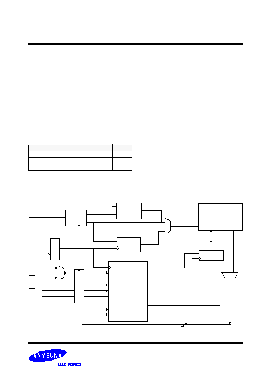
GENERAL DESCRIPTION
FEATURES
LOGIC BLOCK DIAGRAM
·
3.3V+0.165V/-0.165V Power Supply.
· I/O Supply Voltage 3.3V+0.165V/-0.165V for 3.3V I/O
or 2.5V+0.4V/-0.125V for 2.5V I/O
· Byte Writable Function.
·
Enable clock and suspend operation.
·
Single READ/WRITE control pin.
·
Self-Timed Write Cycle.
· Three Chip Enable for simple depth expansion with no data
contention .
·
A interleaved burst or a linear burst mode.
·
Asynchronous output enable control.
· Power Down mode.
·
TTL-Level Three-State Outputs.
·
100-TQFP-1420A .
NtRAM
TM
and No Turnaround Random Access Memory are trademarks of Samsung.
WE
BW
x
CLK
CKE
CS
1
CS
2
CS
2
ADV
OE
ZZ
DQa
0
~ DQd
7
or
DQa
0
~ DQb
8
ADDRESS
ADDRESS
REGISTER
C
O
N
T
R
O
L
L
O
G
I
C
A
0
~A
1
36 or 18
DQPa ~ DQPd
BUFFER
DATA-IN
REGISTER
K
REGISTER
BURST
ADDRESS
COUNTER
WRITE
CONTROL
LOGIC
C
O
N
T
R
O
L
R
E
G
I
S
T
E
R
K
A [0:19]or
A [0:20]
LBO
A
2
~A
19
or
A
2
~A
20
A
0
~A
1
(x=a,b,c,d or a,b)
1Mx36 , 2Mx18
MEMORY
ARRAY
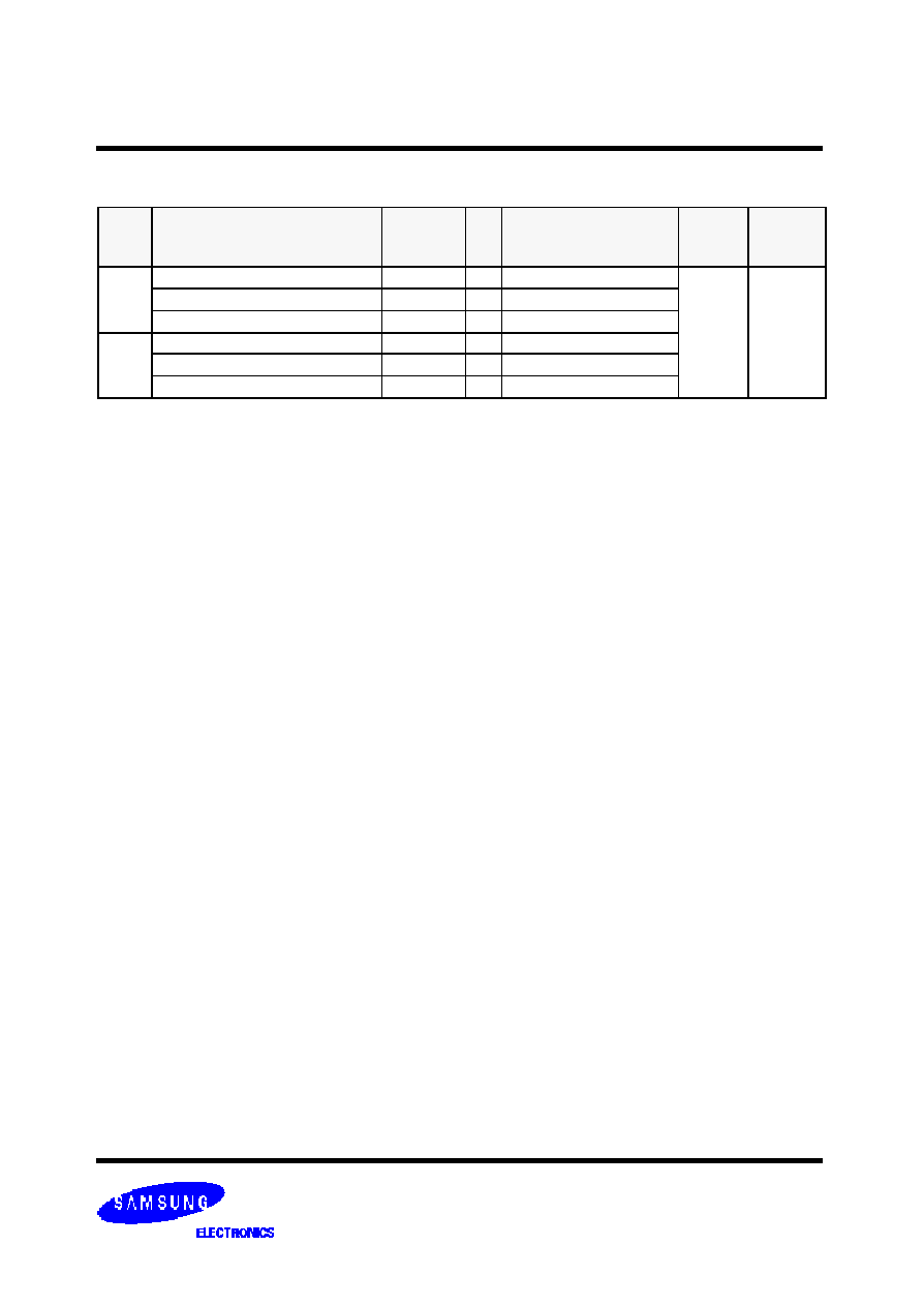
FAST ACCESS TIMES
Parameter
Symbol
-75
Unit
Cycle Time
t
CYC
8.5
ns
Clock Access Time
t
CD
7.5
ns
Output Enable Access Time
t
OE
3.5
ns
1Mx36 & 2Mx18 Flow-Through NtRAM
TM
- 4 -
Rev 2.0
Nov. 2003
K7M321825M
K7M323625M
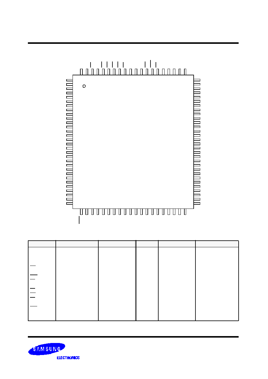
PIN CONFIGURATION
(TOP VIEW)
1
2
3
4
5
6
7
8
9
10
11
12
13
14
15
16
17
18
19
20
21
22
23
24
25
26
27
28
29
30
100 Pin TQFP
(20mm x 14mm)
DQPc
DQc
0
DQc
1
V
DDQ
V
SSQ
DQc
2
DQc
3
DQc
4
DQc
5
V
SSQ
V
DDQ
DQc
6
DQc
7
Vss
V
DD
V
DD
V
SS
DQd
0
DQd
1
V
DDQ
V
SSQ
DQd
2
DQd
3
DQd
4
DQd
5
V
SSQ
V
DDQ
DQd
6
DQd
7
DQPd
80
79
78
77
76
75
74
73
72
71
70
69
68
67
66
65
64
63
62
61
60
59
58
57
56
55
54
53
52
51
DQPb
DQb
7
DQb
6
V
DDQ
V
SSQ
DQb
5
DQb
4
DQb
3
DQb
2
V
SSQ
V
DDQ
DQb
1
DQb
0
V
SS
V
DD
ZZ
DQa
7
DQa
6
V
DDQ
V
SSQ
DQa
5
DQa
4
DQa
3
DQa
2
V
SSQ
V
DDQ
DQa
1
DQa
0
DQPa
1
0
0
9
9
9
8
9
7
9
6
9
5
9
4
9
3
9
2
9
1
9
0
8
9
8
8
8
7
8
6
8
5
8
4
8
3
8
2
A
6
A
7
C
S
1
C
S
2
B
W
d
B
W
c
B
W
b
B
W
a
C
S
2
V
D
D
V
S
S
C
L
K
W
E
C
K
E
O
E
A
D
V
A
1
8
A
1
7
A
8
8
1
A
9
5
0
4
9
4
8
4
7
4
6
4
5
4
4
4
3
4
2
4
1
4
0
3
9
3
8
3
7
3
6
3
5
3
4
3
3
3
2
A
1
6
A
1
5
A
1
4
A
1
3
A
1
2
A
1
1
A
1
0
A
1
9
N
.
C
.
V
D
D
V
S
S
N
.
C
.
N
.
C
.
A
0
A
1
A
2
A
3
A
4
A
5
3
1
L
B
O
PIN NAME
Notes :
1. A
0
and A
1
are the two least significant bits(LSB) of the address field and set the internal burst counter if burst is desired.
SYMBOL
PIN NAME
TQFP PIN NO.
SYMBOL
PIN NAME
TQFP PIN NO.
A
0
- A
19
ADV
W E
CLK
CKE
CS
1
CS
2
CS
2
B Wx(x=a,b,c,d)
OE
ZZ
LBO
Address Inputs
Address Advance/Load
Read/Write Control Input
Clock
Clock Enable
Chip Select
Chip Select
Chip Select
Byte Write Inputs
Output Enable
Power Sleep Mode
Burst Mode Control
32,33,34,35,36,37,43
4445,46,47,48,49,50,
81,82,83,84,99,100
85
88
89
87
98
97
92
93,94,95,96
86
64
31
V
DD
V
SS
N.C.
DQa
0
~a
7
DQb
0
~b
7
DQc
0
~c
7
DQd
0
~d
7
DQPa~P
d
V
DDQ
V
SSQ
Power Supply(+3.3V)
Ground
No Connect
Data Inputs/Outputs
Data Inputs/Outputs
Data Inputs/Outputs
Data Inputs/Outputs
Data Inputs/Outputs
Output Power Supply
(2.5V or 3.3V)
Output Ground
15,16,41,65,91
14,17,40,66,67,90
38,39,42
52,53,56,57,58,59,62,63
68,69,72,73,74,75,78,79
2,3,6,7,8,9,12,13
18,19,22,23,24,25,28,29
51,80,1,30
4,11,20,27,54,61,70,77
5,10,21,26,55,60,71,76
K7M323625M(1Mx36)
V
SS
1Mx36 & 2Mx18 Flow-Through NtRAM
TM
- 5 -
Rev 2.0
Nov. 2003
K7M321825M
K7M323625M
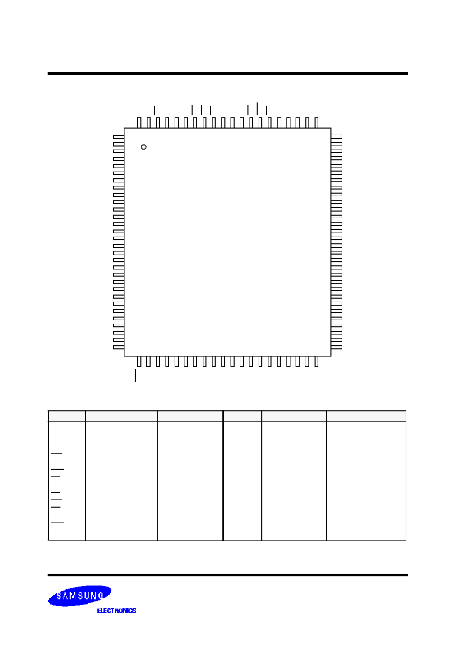
PIN CONFIGURATION
(TOP VIEW)
1
2
3
4
5
6
7
8
9
10
11
12
13
14
15
16
17
18
19
20
21
22
23
24
25
26
27
28
29
30
100 Pin TQFP
(20mm x 14mm)
N.C.
N.C.
N.C.
V
DDQ
V
SSQ
N.C.
N.C.
DQb
8
DQb
7
V
SSQ
V
DDQ
DQb
6
DQb
5
V
SS
V
DD
V
DD
V
SS
DQb
4
DQb
3
V
DDQ
V
SSQ
DQb
2
DQb
1
DQb
0
N.C.
V
SSQ
V
DDQ
N.C.
N.C.
N.C.
80
79
78
77
76
75
74
73
72
71
70
69
68
67
66
65
64
63
62
61
60
59
58
57
56
55
54
53
52
51
A
10
N.C.
N.C.
V
DDQ
V
SSQ
N.C.
DQa
0
DQa
1
DQa
2
V
SSQ
V
DDQ
DQa
3
DQa
4
V
SS
V
SS
V
DD
ZZ
DQa
5
DQa
6
V
DDQ
V
SSQ
DQa
7
DQa
8
N.C.
N.C.
V
SSQ
V
DDQ
N.C.
N.C.
N.C.
1
0
0
9
9
9
8
9
7
9
6
9
5
9
4
9
3
9
2
9
1
9
0
8
9
8
8
8
7
8
6
8
5
8
4
8
3
8
2
A
6
A
7
C
S
1
C
S
2
B
W
b
B
W
a
C
S
2
V
D
D
V
S
S
C
L
K
W
E
C
K
E
O
E
A
D
V
A
1
9
A
1
8
A
8
8
1
A
9
5
0
4
9
4
8
4
7
4
6
4
5
4
4
4
3
4
2
4
1
4
0
3
9
3
8
3
7
3
6
3
5
3
4
3
3
3
2
A
1
7
A
1
6
A
1
5
A
1
4
A
1
3
A
1
2
A
1
1
A
2
0
N
.
C
.
V
D
D
V
S
S
N
.
C
.
N
.
C
.
A
0
A
1
A
2
A
3
A
4
A
5
3
1
L
B
O
K7M321825M(2Mx18)
N
.
C
.
N
.
C
.
PIN NAME
Notes :
1. A
0
and A
1
are the two least significant bits(LSB) of the address field and set the internal burst counter if burst is desired.
SYMBOL
PIN NAME
TQFP PIN NO.
SYMBOL
PIN NAME
TQFP PIN NO.
A
0
- A
20
ADV
WE
CLK
CKE
CS
1
CS
2
CS
2
BW x(x=a,b)
OE
ZZ
LBO
Address Inputs
Address Advance/Load
Read/Write Control Input
Clock
Clock Enable
Chip Select
Chip Select
Chip Select
Byte Write Inputs
Output Enable
Power Sleep Mode
Burst Mode Control
32,33,34,35,36,37,43
44,45,46,47,48,49,50,
80,81,82,83,84,99,100
85
88
89
87
98
97
92
93,94
86
64
31
V
DD
V
SS
N.C.
DQa
0
~a
8
DQb
0
~b
8
V
DDQ
V
SSQ
Power Supply(+3.3V)
Ground
No Connect
Data Inputs/Outputs
Data Inputs/Outputs
Output Power Supply
(2.5V or 3.3V)
Output Ground
15,16,41,65,91
14,17,40,66,67,90
1,2,3,6,7,25,28,29,30,
38,39,42,51,52,53,
56,57,75,78,79,95,96
58,59,62,63,68,69,72,73,74
8,9,12,13,18,19,22,23,24
4,11,20,27,54,61,70,77
5,10,21,26,55,60,71,76