
K7M403625B
128Kx36/x32 & 256Kx18 Flow-Through NtRAM
TM
- 1 -
Rev 1.0
November 2001
K7M401825B
K7M403225B
Document Title
128Kx36 & 128Kx32 & 256Kx18-Bit Flow Through NtRAM
TM
The attached data sheets are prepared and approved by SAMSUNG Electronics. SAMSUNG Electronics CO., LTD. reserve the right to change the
specifications. SAMSUNG Electronics will evaluate and reply to your requests and questions on the parameters of this device. If you have any ques-
tions, please contact the SAMSUNG branch office near your office, call or contact Headquarters.
Revision History
Rev. No.
0.0
0.1
0.2
1.0
Remark
Preliminary
Preliminary
Preliminary
Final
History
1. Initial document.
1. Changed DC parameters
Icc ; from 300mA to 250mA at -65,
from 280mA to 230mA at -75,
from 260mA to 210mA at -80,
from 240mA to 190mA at -90,
I
SB
; from 140mA to 130mA at -65,
from 130mA to 120mA at -75,
from 120mA to 110mA at -80,
from 110mA to 100mA at -90,
I
SB1
; from 100mA to 80mA
1. Add x32 org. and industrial temperature
1. Final spec release
2. Changed Pin Capacitance
- Cin ; from 5pF to 4pF
- Cout ; from 7pF to 6pF
Draft Date
May. 15. 2001
June. 12. 2001
Aug. 11. 2001
Nov. 15. 2001
K7M403625B
128Kx36/x32 & 256Kx18 Flow-Through NtRAM
TM
- 2 -
Rev 1.0
November 2001
K7M401825B
K7M403225B
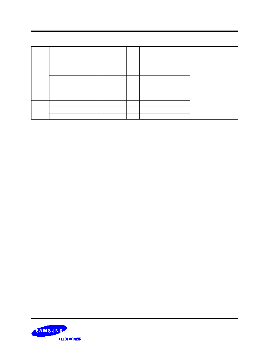
4Mb NtRAM(Flow Through / Pipelined) Ordering Information
Org.
Part Number
Mode
VDD
Speed
FT ; Access Time(ns)
Pipelined ; Cycle Time(MHz)
PKG
Temp
256Kx18
K7M401825B-QC(I)65/75/80
FlowThrough
3.3
6.5/7.5/8.0 ns
Q :100TQFP
C
(Commercial
Temperature
Range)
I:
(Industrial
Temperature
Range)
K7N401801B-QC(I)16/13
Pipelined
3.3
167/133 MHz
K7N401809B-QC(I)25/22/20
Pipelined
3.3
250/225/200 MHz
128Kx32
K7M403225B-QC(I)65/75/80
FlowThrough
3.3
6.5/7.5/8.0 ns
K7N403201B-QC(I)16/13
Pipelined
3.3
167/133 MHz
K7N403209B-QC(I)25/22/20
Pipelined
3.3
250/225/200 MHz
128Kx36
K7M403625B-QC(I)65/75/80
FlowThrough
3.3
6.5/7.5/8.0 ns
K7N403601B-QC(I)16/13
Pipelined
3.3
167/133 MHz
K7N403609B-QC(I)25/22/20
Pipelined
3.3
250/225/200 MHz
K7M403625B
128Kx36/x32 & 256Kx18 Flow-Through NtRAM
TM
- 3 -
Rev 1.0
November 2001
K7M401825B
K7M403225B
128Kx36 & 128Kx32 & 256Kx18-Bit Flow-Through NtRAM
TM
The K7M403625B, K7M403225B and K7M401825B are
4,718,592-bit Synchronous Static SRAMs.
The NtRAM
TM
, or No Turnaround Random Access Memory uti-
lizes all bandwidth in any combination of operating cycles.
Address, data inputs, and all control signals except output
enable and linear burst order are synchronized to input clock.
Burst order control must be tied "High or Low".
Asynchronous inputs include the sleep mode enable(ZZ).
Output Enable controls the outputs at any given time.
Write cycles are internally self-timed and initiated by the rising
edge of the clock input. This feature eliminates complex off-chip
write pulse generation
and provides increased timing flexibility for incomming signals.
For read cycles, Flow-Through SRAM allows output data to
simply flow freely from the memory array.
The K7M403625B, K7M403225B and K7M401825B are imple-
mented with SAMSUNG
s high performance CMOS technology
and is available in 100pin TQFP packages. Multiple power and
ground pins minimize ground bounce.
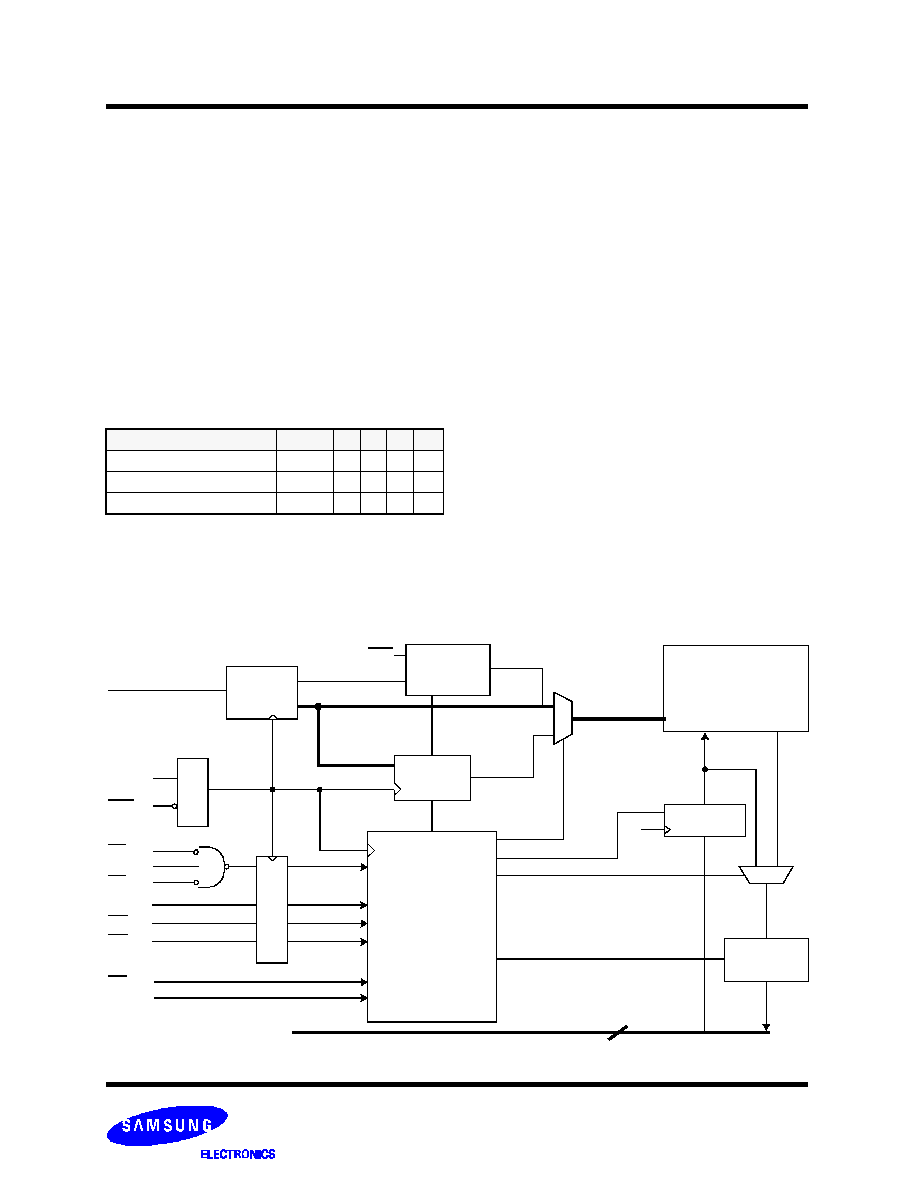
GENERAL DESCRIPTION
FEATURES
LOGIC BLOCK DIAGRAM
∑ V
DD
=3.3V+0.165V/-0.165V Power Supply.
∑ V
DDQ
Supply Voltage 3.3V+0.165V/-0.165V for 3.3V I/O
or 2.5V+0.4V/-0.125V for 2.5V I/O.
∑ Byte Writable Function.
∑
Enable clock and suspend operation.
∑
Single READ/WRITE control pin.
∑
Self-Timed Write Cycle.
∑ Three Chip Enable for simple depth expansion with no data
contention
∑
A interleaved burst or a linear burst mode.
∑
Asynchronous output enable control.
∑ Power Down mode.
∑
TTL-Level Three-State Outputs.
∑
100-TQFP-1420A Package.
∑ Operating in commeical and industrial temperature range.
FAST ACCESS TIMES
PARAMETER
Symbol
-65 -75 -80 Unit
Cycle Time
t
CYC
7.5
8.5
10
ns
Clock Access Time
t
CD
6.5
7.5
8.0
ns
Output Enable Access Time
t
OE
3.5
3.5
4.0
ns
WE
BW
x
CLK
CKE
CS
1
CS
2
CS
2
ADV
OE
ZZ
DQa
0
~ DQd
7
or
DQa
0
~ DQb
8
ADDRESS
128Kx36/32 , 256Kx18
MEMORY
ARRAY
C
O
N
T
R
O
L
L
O
G
I
C
A
0
~A
1
36 /32or 18
DQPa ~ DQPd
BUFFER
DATA-IN
REGISTER
K
REGISTER
BURST
ADDRESS
COUNTER
ADDRESS
REGISTER
WRITE
CONTROL
LOGIC
C
O
N
T
R
O
L
R
E
G
I
S
T
E
R
K
A [0:16]or
A [0:17]
LBO
A
2
~A
16
or
A
2
~A
17
A
0
~A
1
(x=a,b,c,d or a,b)
NtRAM
TM
and No Turnaround Random Access Memory are trademarks of Samsung,

K7M403625B
128Kx36/x32 & 256Kx18 Flow-Through NtRAM
TM
- 4 -
Rev 1.0
November 2001
K7M401825B
K7M403225B
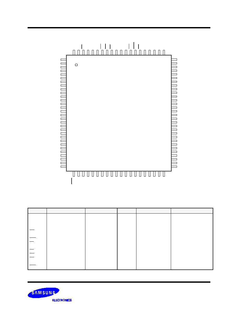
PIN CONFIGURATION
(TOP VIEW)
1
2
3
4
5
6
7
8
9
10
11
12
13
14
15
16
17
18
19
20
21
22
23
24
25
26
27
28
29
30
100 Pin TQFP
(20mm x 14mm)
DQPc/NC
DQc
0
DQc
1
V
DDQ
V
SSQ
DQc
2
DQc
3
DQc
4
DQc
5
V
SSQ
V
DDQ
DQc
6
DQc
7
Vss
V
DD
V
DD
V
SS
DQd
0
DQd
1
V
DDQ
V
SSQ
DQd
2
DQd
3
DQd
4
DQd
5
V
SSQ
V
DDQ
DQd
6
DQd
7
DQPd/NC
80
79
78
77
76
75
74
73
72
71
70
69
68
67
66
65
64
63
62
61
60
59
58
57
56
55
54
53
52
51
DQPb/NC
DQb
7
DQb
6
V
DDQ
V
SSQ
DQb
5
DQb
4
DQb
3
DQb
2
V
SSQ
V
DDQ
DQb
1
DQb
0
V
SS
V
DD
ZZ
DQa
7
DQa
6
V
DDQ
V
SSQ
DQa
5
DQa
4
DQa
3
DQa
2
V
SSQ
V
DDQ
DQa
1
DQa
0
DQPa/NC
1
0
0
9
9
9
8
9
7
9
6
9
5
9
4
9
3
9
2
9
1
9
0
8
9
8
8
8
7
8
6
8
5
8
4
8
3
8
2
A
6
A
7
C
S
1
C
S
2
B
W
d
B
W
c
B
W
b
B
W
a
C
S
2
V
D
D
V
S
S
C
L
K
W
E
C
K
E
O
E
A
D
V
N
.
C
.
N
.
C
.
A
8
8
1
A
9
5
0
4
9
4
8
4
7
4
6
4
5
4
4
4
3
4
2
4
1
4
0
3
9
3
8
3
7
3
6
3
5
3
4
3
3
3
2
A
1
6
A
1
5
A
1
4
A
1
3
A
1
2
A
1
1
A
1
0
N
.
C
.
N
.
C
.
V
D
D
V
S
S
N
.
C
.
N
.
C
.
A
0
A
1
A
2
A
3
A
4
A
5
3
1
L
B
O
PIN NAME
Notes : 1. The pin 83 is reserved for address bit for the 8Mb NtRAM.
2. A
0
and A
1
are the two least significant bits(LSB) of the address field and set the internal burst counter if burst is desired.
3. DQPa~Pd pins are NC for K7N403225B
SYMBOL
PIN NAME
TQFP PIN NO.
SYMBOL
PIN NAME
TQFP PIN NO.
A
0
- A
16
ADV
WE
CLK
CKE
CS
1
CS
2
CS
2
BWx(x=a,b,c,d)
OE
ZZ
LBO
Address Inputs
Address Advance/Load
Read/Write Control Input
Clock
Clock Enable
Chip Select
Chip Select
Chip Select
Byte Write Inputs
Output Enable
Power Sleep Mode
Burst Mode Control
32,33,34,35,36,37
44,45,46,47,48,49
50,81,82,99,100
85
88
89
87
98
97
92
93,94,95,96
86
64
31
V
DD
V
SS
N.C.
DQa
0
~a
7
DQb
0
~b
7
DQc
0
~c
7
DQd
0
~d
7
DQPa~P
d
/NC
V
DDQ
V
SSQ
Power Supply(+3.3V)
Ground
No Connect
Data Inputs/Outputs
Output Power Supply
(2.5V or 3.3V)
Output Ground
15,16,41,65,91
14,17,40,66,67,90
38,39,42,43,83,84
52,53,56,57,58,59,62,63
68,69,72,73,74,75,78,79
2,3,6,7,8,9,12,13
18,19,22,23,24,25,28,29
51,80,1,30
4,11,20,27,54,61,70,77
5,10,21,26,55,60,71,76
K7M403625B(128Kx36)
V
SS
K7M403225B(128Kx32)
K7M403625B
128Kx36/x32 & 256Kx18 Flow-Through NtRAM
TM
- 5 -
Rev 1.0
November 2001
K7M401825B
K7M403225B
PIN CONFIGURATION
(TOP VIEW)
1
2
3
4
5
6
7
8
9
10
11
12
13
14
15
16
17
18
19
20
21
22
23
24
25
26
27
28
29
30
100 Pin TQFP
(20mm x 14mm)
N.C.
N.C.
N.C.
V
DDQ
V
SSQ
N.C.
N.C.
DQb
8
DQb
7
V
SSQ
V
DDQ
DQb
6
DQb
5
V
SS
V
DD
V
DD
V
SS
DQb
4
DQb
3
V
DDQ
V
SSQ
DQb
2
DQb
1
DQb
0
N.C.
V
SSQ
V
DDQ
N.C.
N.C.
N.C.
80
79
78
77
76
75
74
73
72
71
70
69
68
67
66
65
64
63
62
61
60
59
58
57
56
55
54
53
52
51
A
10
N.C.
N.C.
V
DDQ
V
SSQ
N.C.
DQa
0
DQa
1
DQa
2
V
SSQ
V
DDQ
DQa
3
DQa
4
V
SS
V
SS
V
DD
ZZ
DQa
5
DQa
6
V
DDQ
V
SSQ
DQa
7
DQa
8
N.C.
N.C.
V
SSQ
V
DDQ
N.C.
N.C.
N.C.
1
0
0
9
9
9
8
9
7
9
6
9
5
9
4
9
3
9
2
9
1
9
0
8
9
8
8
8
7
8
6
8
5
8
4
8
3
8
2
A
6
A
7
C
S
1
C
S
2
B
W
b
B
W
a
C
S
2
V
D
D
V
S
S
C
L
K
W
E
C
K
E
O
E
A
D
V
N
.
C
.
N
.
C
.
A
8
8
1
A
9
5
0
4
9
4
8
4
7
4
6
4
5
4
4
4
3
4
2
4
1
4
0
3
9
3
8
3
7
3
6
3
5
3
4
3
3
3
2
A
1
7
A
1
6
A
1
5
A
1
4
A
1
3
A
1
2
A
1
1
N
.
C
.
N
.
C
.
V
D
D
V
S
S
N
.
C
.
N
.
C
.
A
0
A
1
A
2
A
3
A
4
A
5
3
1
L
B
O
K7M401825B(256Kx18)
N
.
C
.
N
.
C
.
PIN NAME
Notes : 1. The pin 83 is reserved for address bit for the 8Mb NtRAM.
2. A
0
and A
1
are the two least significant bits(LSB) of the address field and set the internal burst counter if burst is desired.
SYMBOL
PIN NAME
TQFP PIN NO.
SYMBOL
PIN NAME
TQFP PIN NO.
A
0
- A
17
ADV
WE
CLK
CKE
CS
1
CS
2
CS
2
BWx(x=a,b)
OE
ZZ
LBO
Address Inputs
Address Advance/Load
Read/Write Control Input
Clock
Clock Enable
Chip Select
Chip Select
Chip Select
Byte Write Inputs
Output Enable
Power Sleep Mode
Burst Mode Control
32,33,34,35,36,37,44
45,46,47,48,49,50,80
81,82,99,100
85
88
89
87
98
97
92
93,94
86
64
31
V
DD
V
SS
N.C.
DQa
0
~a
8
DQb
0
~b
8
V
DDQ
V
SSQ
Power Supply(+3.3V)
Ground
No Connect
Data Inputs/Outputs
Output Power Supply
(2.5V or 3.3V)
Output Ground
15,16,41,65,91
14,17,40,66,67,90
1,2,3,6,7,25,28,29,30,38,39,
42,43,51,52,53,56,57,75,78,
79,83,84,95,96
58,59,62,63,68,69,72,73,74
8,9,12,13,18,19,22,23,24
4,11,20,27,54,61,70,77
5,10,21,26,55,60,71,76
K7M403625B
128Kx36/x32 & 256Kx18 Flow-Through NtRAM
TM
- 6 -
Rev 1.0
November 2001
K7M401825B
K7M403225B
FUNCTION DESCRIPTION
The K7M4036/3225B and K7M401825B are NtRAM
TM
designed to sustain 100% bus bandwidth by eliminating turnaround cycle
when there is transition from Read to Write, or vice versa.
All inputs (with the exception of OE, LBO and ZZ) are synchronized to rising clock edges.
All read, write and deselect cycles are initiated by the ADV input. Subsequent burst addresses can be internally generated by the
burst advance pin (ADV). ADV should be driven to Low once the device has been deselected in order to load a new address for next
operation.
Clock Enable(CKE) pin allows the operation of the chip to be suspended as long as necessary. When CKE is high, all synchronous
inputs are ignored and the internal device registers will hold their previous values.
NtRAM
TM
latches external address and initiates a cycle, when CKE, ADV are driven to low and all three chip enables(CS
1
, CS
2
, CS
2
)
are active .
Output Enable(OE) can be used to disable the output at any given time.
Read operation is initiated when at the rising edge of the clock, the address presented to the address inputs are latched in the
address register, CKE is driven low, all three chip enables(CS
1
, CS
2
, CS
2
) are active, the write enable input signals WE are driven
high, and ADV driven low. Data appears at the outputs within the same clock cycle as the address for the data. Also during read oper-
ation OE must be driven low for the device to drive out the requested data.
Write operation occurs when WE is driven low at the rising edge of the clock. BW[d:a] can be used for byte write operation. The Flow
Through NtRAM
TM
uses a late write cycle to utilize 100% of the bandwidth.
At the first rising edge of the clock, WE and address are registered, and the data associated with that address is required one cycle
later.
Subsequent addresses are generated by ADV High for the burst access as shown below. The starting point of the burst seguence is
provided by the external address. The burst address counter wraps around to its initial state upon completion.
The burst sequence is determined by the state of the LBO pin. When this pin is low, linear burst sequence is selected.
And when this pin is high, Interleaved burst sequence is selected.
During normal operation, ZZ must be driven low. When ZZ is driven high, the SRAM will enter a Power Sleep Mode after 2 cycles. At
this time, internal state of the SRAM is preserved. When ZZ returns to low, the SRAM normally operates after 2 cycles of wake up
time.
BURST SEQUENCE TABLE
(Interleaved Burst, LBO=High)
Notes : 1. LBO pin must be tied to High or Low, and Floating State must not be allowed
.
LBO PIN
HIGH
Case 1
Case 2
Case 3
Case 4
A
1
A
0
A
1
A
0
A
1
A
0
A
1
A
0
First Address
Fourth Address
0
0
1
1
0
1
0
1
0
0
1
1
1
0
1
0
1
1
0
0
0
1
0
1
1
1
0
0
1
0
1
0
BQ TABLE
(Linear Burst, LBO=Low)
Notes : 1. LBO pin must be tied to High or Low, and Floating State must not be allowed
.
LBO PIN
LOW
Case 1
Case 2
Case 3
Case 4
A
1
A
0
A
1
A
0
A
1
A
0
A
1
A
0
First Address
Fourth Address
0
0
1
1
0
1
0
1
0
1
1
0
1
0
1
0
1
1
0
0
0
1
0
1
1
0
0
1
1
0
1
0
K7M403625B
128Kx36/x32 & 256Kx18 Flow-Through NtRAM
TM
- 7 -
Rev 1.0
November 2001
K7M401825B
K7M403225B
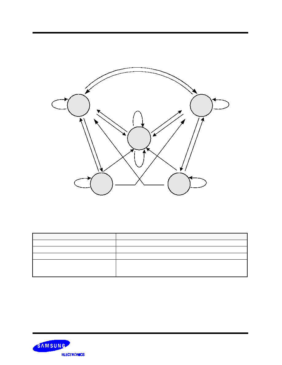
STATE DIAGRAM FOR NtRAM
TM
BEGIN
WRITE
BURST
WRITE
BEGIN
READ
WRITE
DS
RE
AD
BURST
READ
DS
WR
ITE
DS
READ
DS
R
E
A
D
D
S
W
R
IT
E
B
U
R
S
T
DESELECT
B
U
R
S
T
R
E
A
D
B
U
R
S
T
W
R
IT
E
READ
WRITE
BURST
BURST
Notes : 1. An IGNORE CLOCK EDGE cycle is not shown is the above diagram. This is because CKE HIGH only blocks the clock(CLK) input and does
not change the state of the device.
2. States change on the rising edge of the clock(CLK)
COMMAND
ACTION
DS
DESELECT
READ
BEGIN READ
WRITE
BEGIN WRITE
BURST
BEGIN READ
BEGIN WRITE
CONTINUE DESELECT
K7M403625B
128Kx36/x32 & 256Kx18 Flow-Through NtRAM
TM
- 8 -
Rev 1.0
November 2001
K7M401825B
K7M403225B
SYNCHRONOUS TRUTH TABLE
Notes : 1. X means "Don
t Care". 2. The rising edge of clock is symbolized by (
).
3. A continue deselect cycle can only be enterd if a deselect cycle is executed first.
4. WRITE = L means Write operation in WRITE TRUTH TABLE.
WRITE = H means Read operation in WRITE TRUTH TABLE.
5. Operation finally depends on status of asynchronous input pins(ZZ and OE).
CS
1
CS
2
CS
2
ADV
WE
BWx
OE
CKE
CLK
ADDRESS ACCESSED
OPERATION
H
X
X
L
X
X
X
L
N/A
Not Selected
X
L
X
L
X
X
X
L
N/A
Not Selected
X
X
H
L
X
X
X
L
N/A
Not Selected
X
X
X
H
X
X
X
L
N/A
Not Selected Continue
L
H
L
L
H
X
L
L
External Address
Begin Burst Read Cycle
X
X
X
H
X
X
L
L
Next Address
Continue Burst Read Cycle
L
H
L
L
H
X
H
L
External Address
NOP/Dummy Read
X
X
X
H
X
X
H
L
Next Address
Dummy Read
L
H
L
L
L
L
X
L
External Address
Begin Burst Write Cycle
X
X
X
H
X
L
X
L
Next Address
Continue Burst Write Cycle
L
H
L
L
L
H
X
L
N/A
NOP/Write Abort
X
X
X
H
X
H
X
L
Next Address
Write Abort
X
X
X
X
X
X
X
H
Current Address
Ignore Clock
WRITE TRUTH TABLE
(x36/32)
Notes : 1. X means "Don
t Care".
2. All inputs in this table must meet setup and hold time around the rising edge of CLK(
).
WE
BWa
BWb
BWc
BWd
OPERATION
H
X
X
X
X
READ
L
L
H
H
H
WRITE BYTE a
L
H
L
H
H
WRITE BYTE b
L
H
H
L
H
WRITE BYTE c
L
H
H
H
L
WRITE BYTE d
L
L
L
L
L
WRITE ALL BYTEs
L
H
H
H
H
WRITE ABORT/NOP
TRUTH TABLES
WRITE TRUTH TABLE
(x18)
Notes : 1. X means "Don
t Care".
2. All inputs in this table must meet setup and hold time around the rising edge of CLK(
).
WE
BWa
BWb
OPERATION
H
X
X
READ
L
L
H
WRITE BYTE a
L
H
L
WRITE BYTE b
L
L
L
WRITE ALL BYTEs
L
H
H
WRITE ABORT/NOP
K7M403625B
128Kx36/x32 & 256Kx18 Flow-Through NtRAM
TM
- 9 -
Rev 1.0
November 2001
K7M401825B
K7M403225B
ASYNCHRONOUS TRUTH TABLE
OPERATION
ZZ
OE
I/O STATUS
Sleep Mode
H
X
High-Z
Read
L
L
DQ
L
H
High-Z
Write
L
X
Din, High-Z
Deselected
L
X
High-Z
Notes
1. X means "Don
t Care".
2. Sleep Mode means power Sleep Mode of which stand-by current does
not depend on cycle time.
3. Deselected means power Sleep Mode of which stand-by current
depends on cycle time.
CAPACITANCE*
(T
A
=25
∞
C, f=1MHz)
*Note : Sampled not 100% tested.
PARAMETER
SYMBOL
TEST CONDITION
MIN
MAX
UNIT
Input Capacitance
C
IN
V
IN
=0V
-
4
pF
Output Capacitance
C
OUT
V
OUT
=0V
-
6
pF
OPERATING CONDITIONS at 3.3V I/O
(0
∞
C
T
A
70
∞
C)
* The above parameters are also guaranteed at industrial temperature range.
PARAMETER
SYMBOL
MIN
Typ.
MAX
UNIT
Supply Voltage
V
DD
3.135
3.3
3.465
V
V
DDQ
3.135
3.3
3.465
V
Ground
V
SS
0
0
0
V
OPERATING CONDITIONS at 2.5V I/O
(0
∞
C
T
A
70
∞
C)
* The above parameters are also guaranteed at industrial temperature range.
PARAMETER
SYMBOL
MIN
Typ.
MAX
UNIT
Supply Voltage
V
DD
3.135
3.3
3.465
V
V
DDQ
2.375
2.5
2.9
V
Ground
V
SS
0
0
0
V
ABSOLUTE MAXIMUM RATINGS*
*Note : Stresses greater than those listed under "Absolute Maximum Ratings" may cause permanent damage to the device. This is a stress rating only
and functional operation of the device at these or any other conditions above those indicated in the operating sections of this specification is not
implied. Exposure to absolute maximum rating conditions for extended periods may affect reliability.
PARAMETER
SYMBOL
RATING
UNIT
Voltage on V
DD
Supply Relative to V
SS
Voltage on V
DDQ
Supply Relative to V
SS
V
DD
-0.3 to 4.6
V
V
DDQ
V
DD
V
Voltage on Input Pin Relative to V
SS
V
IN
-0.3 to V
DD
+0.3
V
Voltage on I/O Pin Relative to V
SS
V
IO
-0.3 to V
DDQ
+0.3
V
Power Dissipation
P
D
1.4
W
Storage Temperature
T
STG
-65 to 150
∞
C
Operating Temperature
Commercial
T
OPR
0 to 70
∞
C
Industrial
T
OPR
-40 to 85
∞
C
Storage Temperature Range Under Bias
T
BIAS
-10 to 85
∞
C
K7M403625B
128Kx36/x32 & 256Kx18 Flow-Through NtRAM
TM
- 10 -
Rev 1.0
November 2001
K7M401825B
K7M403225B
V
SS
V
IH
V
SS-
1.0V
20% t
CYC
(MIN)
DC ELECTRICAL CHARACTERISTICS
(V
DD
=3.3V+0.165V/-0.165V, T
A
=0
∞
C to +70
∞
C)
Notes : 1. The above parameters are also guaranteed at industrial temperature range.
2. Reference AC Operating Conditions and Characteristics for input and timing.
3. Data states are all zero.
4. In Case of I/O Pins, the Max. V
IH
=V
DDQ
+0.3V
PARAMETER
SYMBOL
TEST CONDITIONS
MIN
MAX
UNIT
NOTES
Input Leakage Current(except ZZ)
I
IL
V
DD
=Max ; V
IN
=V
SS
to V
DD
-2
+2
µ
A
Output Leakage Current
I
OL
Output Disabled,
-2
+2
µ
A
Operating Current
I
CC
V
DD
=Max
I
OUT
=0mA
Cycle Time
t
CYC
Min
-65
-
250
mA
1,2
-75
-
230
-80
-
210
Standby Current
I
SB
Device deselected, I
OUT
=0mA,
ZZ
V
IL
, f=Max,
All Inputs
0.2V or
V
DD
-0.2V
-65
-
130
mA
-75
-
120
-80
-
110
I
SB1
Device deselected, I
OUT
=0mA, ZZ
0.2V, f=0,
All Inputs=fixed (V
DD
-0.2V or 0.2V)
-
80
mA
I
SB2
Device deselected, I
OUT
=0mA, ZZ
V
DD
-0.2V,
f=Max, All Inputs
V
IL
or
V
IH
-
50
mA
Output Low Voltage(3.3V I/O)
V
OL
I
OL
=8.0mA
-
0.4
V
Output High Voltage(3.3V I/O)
V
OH
I
OH
=-4.0mA
2.4
-
V
Output Low Voltage(2.5V I/O)
V
OL
I
OL
=1.0mA
-
0.4
V
Output High Voltage(2.5V I/O)
V
OH
I
OH
=-1.0mA
2.0
-
V
Input Low Voltage(3.3V I/O)
V
IL
-0.3*
0.8
V
Input High Voltage(3.3V I/O)
V
IH
2.0
V
DD
+0.3**
V
3
Input Low Voltage(2.5V I/O)
V
IL
-0.3*
0.7
V
Input High Voltage(2.5V I/O)
V
IH
1.7
V
DD
+0.3**
V
3
(V
DD
=3.3V+0.165V/-0.165V,V
DDQ
=3.3V+0.165V/-0.165V or V
DD
=3.3V+0.165V/-0.165V,V
DDQ
=2.5V+0.4V/-0.125V, T
A
=0to70
∞
C)
TEST CONDITIONS
* The above parameters are also guaranteed at industrial temperature range.
PARAMETER
VALUE
Input Pulse Level(for 3.3V I/O)
0 to 3.0V
Input Pulse Level(for 2.5V I/O)
0 to 2.5V
Input Rise and Fall Time(Measured at 20% to 80% for 3.3V I/O)
1.0V/ns
Input Rise and Fall Time(Measured at 20% to 80% for 2.5V I/O)
1.0V/ns
Input and Output Timing Reference Levels for 3.3V I/O
1.5V
Input and Output Timing Reference Levels for 2.5V I/O
V
DDQ
/2
Output Load
See Fig. 1

K7M403625B
128Kx36/x32 & 256Kx18 Flow-Through NtRAM
TM
- 11 -
Rev 1.0
November 2001
K7M401825B
K7M403225B
AC TIMING CHARACTERISTICS
(V
DD
=3.3V+0.165V/-0.165V, T
A
=0
∞
C to +70
∞
C)
Notes : 1. The above parameters are also guaranteed at industrial temperature range.
2. All address inputs must meet the specified setup and hold times for all rising clock(CLK) edges when ADV is sampled low and CS is sampled
low. All other synchronous inputs must meet the specified setup and hold times whenever this device is chip selected.
3. Chip selects must be valid at each rising edge of CLK(when ADV is Low) to remain enabled.
4. A write cycle is defined by WE low having been registerd into the device at ADV Low, A Read cycle is defined by WE High with ADV Low, Both
cases must meet setup and hold times.
5. To avoid bus contention, At a given vlotage and temperature t
LZC
is more than t
HZC.
The soecs as shown do not imply bus contention because t
LZC
is a Min. parameter that is worst case at totally different test conditions
(0
∞
C,3.465V) than t
HZC
, which is a Max. parameter(worst case at 70
∞
C,3.135V)
It is not possible for two SRAMs on the same board to be at such different voltage and temperatue.
PARAMETER
Symbol
-65
-75
-80
UNIT
Min
Max
Min
Max
Min
Max
Cycle Time
t
CYC
7.5
-
8.5
-
10
-
ns
Clock Access Time
t
CD
-
6.5
-
7.5
-
8.0
ns
Output Enable to Data Valid
t
OE
-
3.5
-
3.5
-
4.0
ns
Clock High to Output Low-Z
t
LZC
2.5
-
2.5
-
2.5
-
ns
Output Hold from Clock High
t
OH
2.5
-
2.5
-
2.5
-
ns
Output Enable Low to Output Low-Z
t
LZOE
0
-
0
-
0
-
ns
Output Enable High to Output High-Z
t
HZOE
-
3.5
-
3.5
-
4.0
ns
Clock High to Output High-Z
t
HZC
-
3.5
-
3.5
-
3.5
ns
Clock High Pulse Width
t
CH
2.5
-
3.0
-
3.0
-
ns
Clock Low Pulse Width
t
CL
2.5
-
3.0
-
3.0
-
ns
Address Setup to Clock High
t
AS
1.5
-
2.0
-
2.0
-
ns
CKE Setup to Clock High
t
CES
1.5
-
2.0
-
2.0
-
ns
Data Setup to Clock High
t
DS
1.5
-
2.0
-
2.0
-
ns
Write Setup to Clock High (WE, BW
X
)
t
WS
1.5
-
2.0
-
2.0
-
ns
Address Advance Setup to Clock High
t
ADVS
1.5
-
2.0
-
2.0
-
ns
Chip Select Setup to Clock High
t
CSS
1.5
-
2.0
-
2.0
-
ns
Address Hold from Clock High
t
AH
0.5
-
0.5
-
0.5
-
ns
CKE Hold from Clock High
t
CEH
0.5
-
0.5
-
0.5
-
ns
Data Hold from Clock High
t
DH
0.5
-
0.5
-
0.5
-
ns
Write Hold from Clock High (WE, BWE
X
)
t
WH
0.5
-
0.5
-
0.5
-
ns
Address Advance Hold from Clock High
t
ADVH
0.5
-
0.5
-
0.5
-
ns
Chip Select Hold from Clock High
t
CSH
0.5
-
0.5
-
0.5
-
ns
ZZ High to Power Down
t
PDS
2
-
2
-
2
-
cycle
ZZ Low to Power Up
t
PUS
2
-
2
-
2
-
cycle
Output Load(B),
(for t
LZC
, t
LZOE
, t
HZOE
& t
HZC
)
Dout
353
/
1538
5pF*
+3.3V for 3.3V I/O
319
/
1667
Fig. 1
* Including Scope and Jig Capacitance
Output Load(A)
Dout
Zo=50
RL=50
VL=1.5V for 3.3V I/O
V
DDQ
/2 for 2.5V I/O
/+2.5V for 2.5V I/O
30pF*
K7M403625B
128Kx36/x32 & 256Kx18 Flow-Through NtRAM
TM
- 12 -
Rev 1.0
November 2001
K7M401825B
K7M403225B
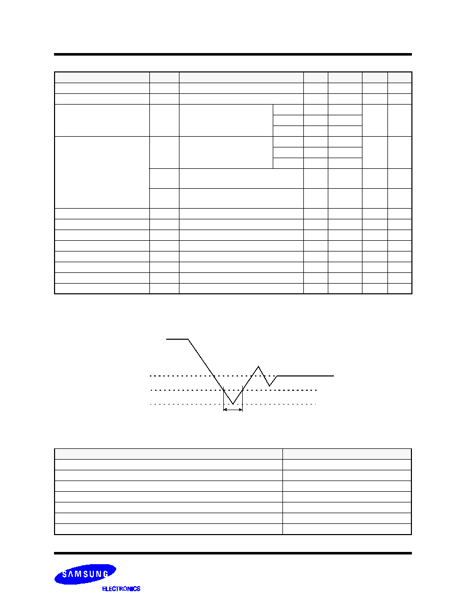
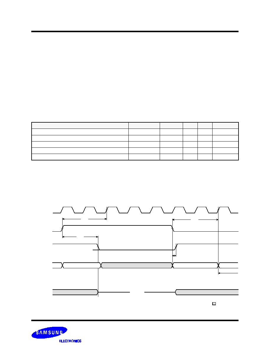
SLEEP MODE
SLEEP MODE is a low current, power-down mode in which the device is deselected and current is reduced to I
SB2
. The duration of
SLEEP MODE is dictated by the length of time the ZZ is in a High state.
After entering SLEEP MODE, all inputs except ZZ become disabled and all outputs go to High-Z
The ZZ pin is an asynchronous, active high input that causes the device to enter SLEEP MODE.
When the ZZ pin becomes a logic High, I
SB2
is guaranteed after the time t
ZZI
is met. Any operation pending when entering SLEEP
MODE is not guaranteed to successful complete. Therefore, SLEEP MODE (READ or WRITE) must not be initiated until valid pend-
ing operations are completed. similarly, when exiting SLEEP MODE during t
PUS
, only a DESELECT or READ cycle should be given
while the SRAM is transitioning out of SLEEP MODE.
SLEEP MODE ELECTRICAL CHARACTERISTICS
DESCRIPTION
CONDITIONS
SYMBOL
MIN
MAX
UNITS
Current during SLEEP MODE
ZZ
V
IH
I
SB2
10
mA
ZZ active to input ignored
t
PDS
2
cycle
ZZ inactive to input sampled
t
PUS
2
cycle
ZZ active to SLEEP current
t
ZZI
2
cycle
ZZ inactive to exit SLEEP current
t
RZZI
0
K
t
PDS
ZZ setup cycle
t
RZZI
ZZ
Isupply
All inputs
(except ZZ)
Outputs
(Q)
t
ZZI
t
PUS
ZZ recovery cycle
Deselect or Read Only
High-Z
DON
T CARE
I
SB2
SLEEP MODE WAVEFORM
Normal
operation
cycle
Deselect or Read Only
K7M403625B
128Kx36/x32 & 256Kx18 Flow-Through NtRAM
TM
- 13 -
Rev 1.0
November 2001
K7M401825B
K7M403225B
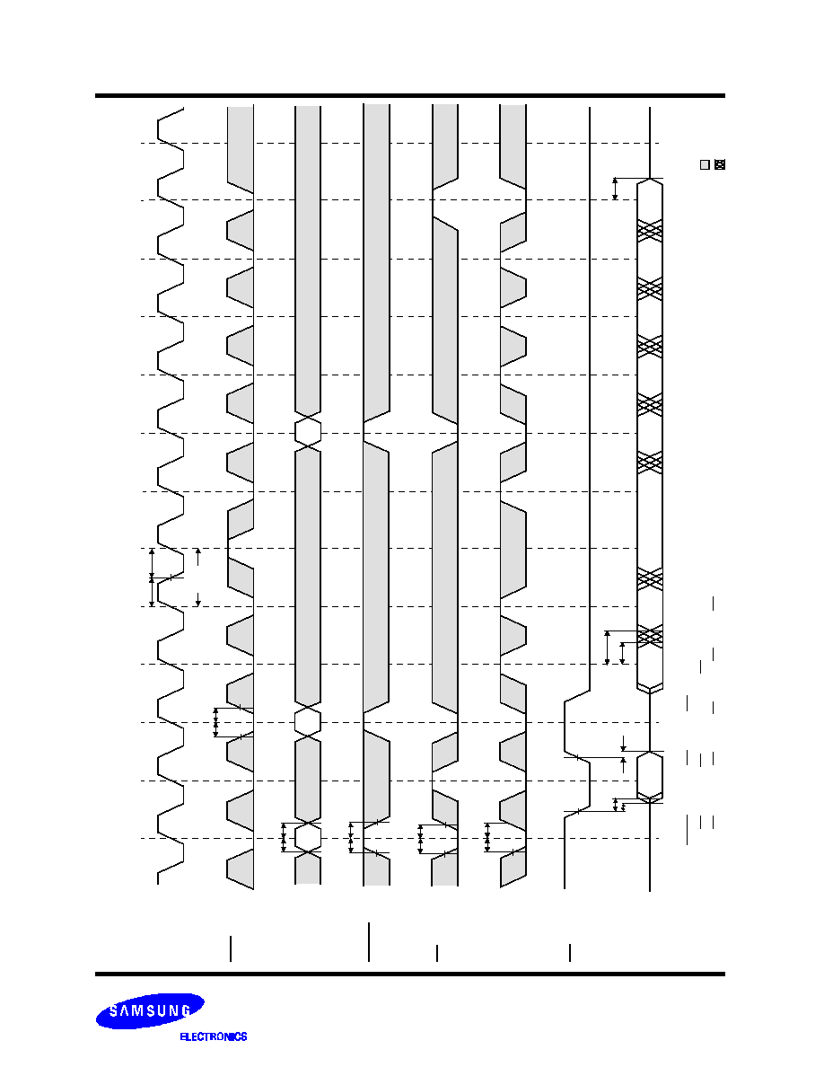
C
l
o
c
k
C
K
E
A
d
d
r
e
s
s
W
R
I
T
E
C
S
A
D
V
O
E
D
a
t
a
O
u
t
T
I
M
I
N
G
W
A
V
E
F
O
R
M
O
F
R
E
A
D
C
Y
C
L
E
N
O
T
E
S
:
W
R
I
T
E
=
L
m
e
a
n
s
W
E
=
L
,
a
n
d
B
W
x
=
L
C
S
=
L
m
e
a
n
s
C
S
1
=
L
,
C
S
2
=
H
a
n
d
C
S
2
=
L
C
S
=
H
m
e
a
n
s
C
S
1
=
H
,
o
r
C
S
1
=
L
a
n
d
C
S
2
=
H
,
o
r
C
S
1
=
L
,
a
n
d
C
S
2
=
L
t
C
H
t
C
L
t
C
E
S
t
C
E
H
t
A
S
t
A
H
A
1
A
2
A
3
t
W
S
t
W
H
t
C
S
S
t
C
S
H
t
O
E
t
H
Z
O
E
t
L
Z
O
E
t
C
D
t
O
H
t
H
Z
C
Q
3
-
4
Q
3
-
3
Q
3
-
2
Q
3
-
1
Q
2
-
4
Q
2
-
3
Q
2
-
2
Q
2
-
1
Q
1
-
1
D
o
n
t
C
a
r
e
U
n
d
e
f
i
n
e
d
t
C
Y
C
t
A
D
V
S
t
A
D
V
H
K7M403625B
128Kx36/x32 & 256Kx18 Flow-Through NtRAM
TM
- 14 -
Rev 1.0
November 2001
K7M401825B
K7M403225B
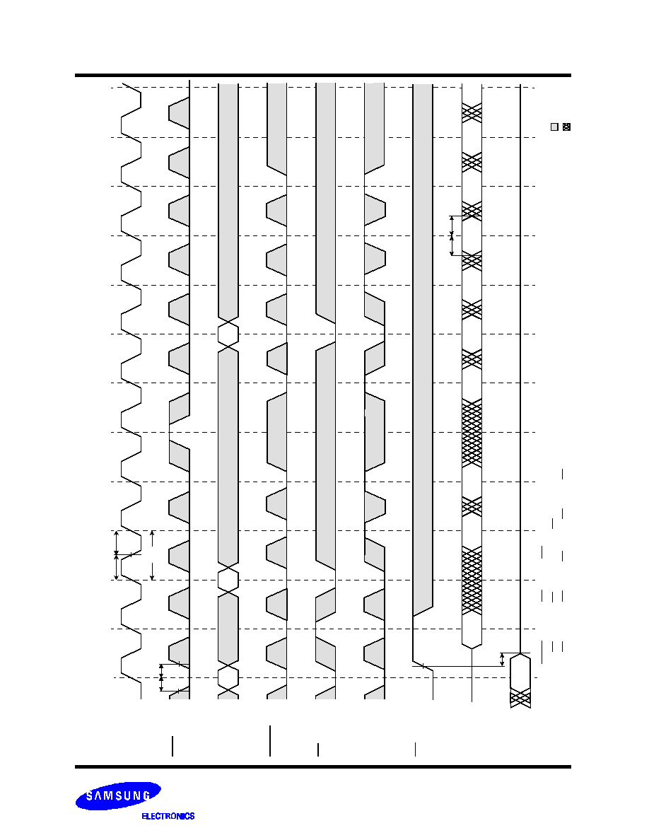
T
I
M
I
N
G
W
A
V
E
F
O
R
M
O
F
W
R
T
E
C
Y
C
L
E
C
l
o
c
k
A
d
d
r
e
s
s
W
R
I
T
E
C
S
A
D
V
D
a
t
a
I
n
t
C
H
t
C
L
A
2
A
3
D
2
-
1
D
1
-
1
D
2
-
2
D
2
-
3
D
2
-
4
D
3
-
1
D
3
-
2
D
3
-
3
O
E
D
a
t
a
O
u
t
t
D
S
t
D
H
t
H
Z
O
E
D
o
n
t
C
a
r
e
U
n
d
e
f
i
n
e
d
t
C
Y
C
C
K
E
A
1
t
C
E
S
t
C
E
H
N
O
T
E
S
:
W
R
I
T
E
=
L
m
e
a
n
s
W
E
=
L
,
a
n
d
B
W
x
=
L
C
S
=
L
m
e
a
n
s
C
S
1
=
L
,
C
S
2
=
H
a
n
d
C
S
2
=
L
C
S
=
H
m
e
a
n
s
C
S
1
=
H
,
o
r
C
S
1
=
L
a
n
d
C
S
2
=
H
,
o
r
C
S
1
=
L
,
a
n
d
C
S
2
=
L
Q
0
-
4
D
3
-
4
K7M403625B
128Kx36/x32 & 256Kx18 Flow-Through NtRAM
TM
- 15 -
Rev 1.0
November 2001
K7M401825B
K7M403225B
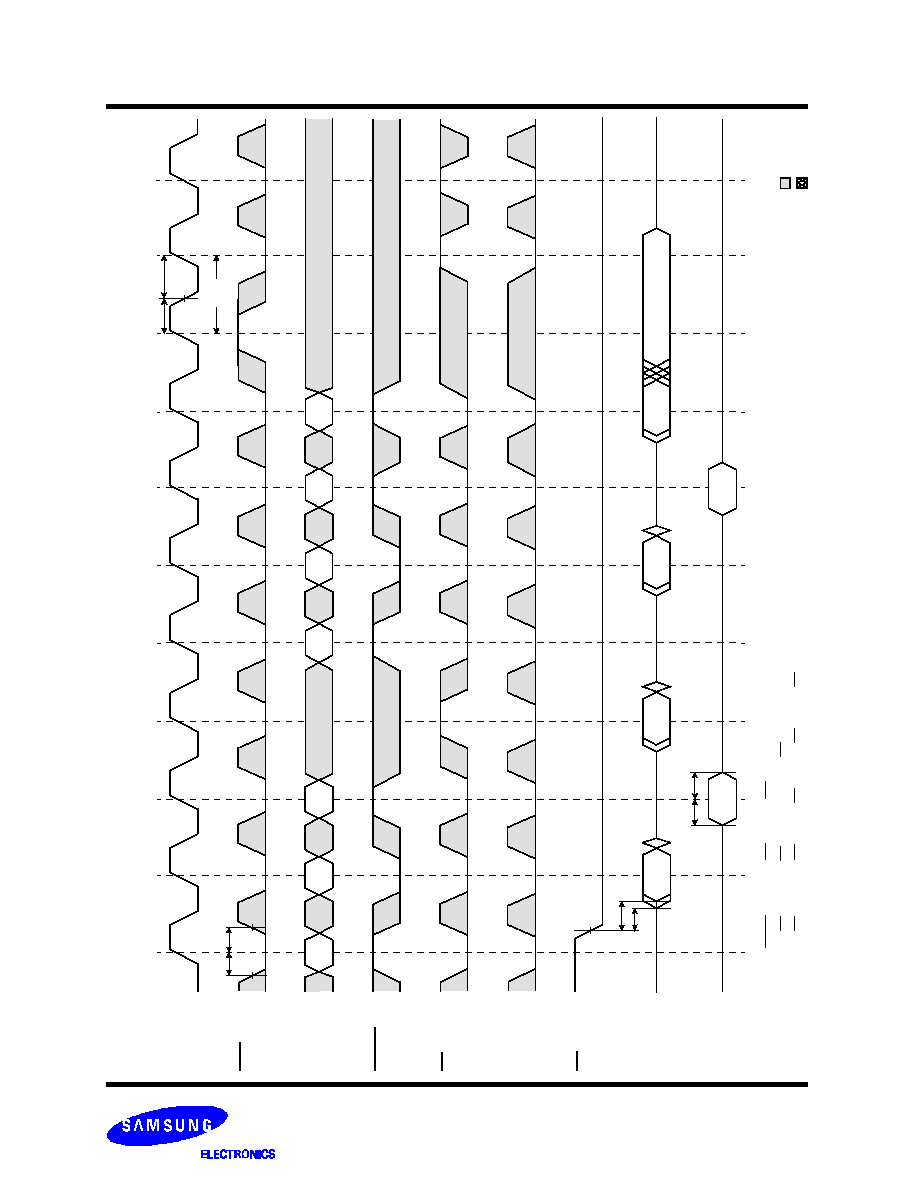
T
I
M
I
N
G
W
A
V
E
F
O
R
M
O
F
S
I
N
G
L
E
R
E
A
D
/
W
R
I
T
E
C
l
o
c
k
A
d
d
r
e
s
s
W
R
I
T
E
C
S
A
D
V
O
E
D
a
t
a
I
n
t
C
H
t
C
L
t
D
S
t
D
H
D
a
t
a
O
u
t
A
2
A
4
A
5
D
2
t
O
E
t
L
Z
O
E
Q
1
D
o
n
t
C
a
r
e
U
n
d
e
f
i
n
e
d
t
C
Y
C
C
K
E
t
C
E
S
t
C
E
H
A
1
A
3
A
7
A
6
Q
3
Q
4
Q
6
D
5
N
O
T
E
S
:
W
R
I
T
E
=
L
m
e
a
n
s
W
E
=
L
,
a
n
d
B
W
x
=
L
C
S
=
L
m
e
a
n
s
C
S
1
=
L
,
C
S
2
=
H
a
n
d
C
S
2
=
L
C
S
=
H
m
e
a
n
s
C
S
1
=
H
,
o
r
C
S
1
=
L
a
n
d
C
S
2
=
H
,
o
r
C
S
1
=
L
,
a
n
d
C
S
2
=
L
Q
7
K7M403625B
128Kx36/x32 & 256Kx18 Flow-Through NtRAM
TM
- 16 -
Rev 1.0
November 2001
K7M401825B
K7M403225B
T
I
M
I
N
G
W
A
V
E
F
O
R
M
O
F
C
K
E
O
P
E
R
A
T
I
O
N
C
l
o
c
k
A
d
d
r
e
s
s
W
R
I
T
E
C
S
A
D
V
O
E
D
a
t
a
I
n
t
C
H
t
C
L
D
a
t
a
O
u
t
A
1
A
2
A
3
A
4
A
5
t
C
E
S
t
C
E
H
D
o
n
t
C
a
r
e
U
n
d
e
f
i
n
e
d
t
C
Y
C
C
K
E
t
D
S
t
D
H
D
2
Q
3
Q
4
Q
1
N
O
T
E
S
:
W
R
I
T
E
=
L
m
e
a
n
s
W
E
=
L
,
a
n
d
B
W
x
=
L
C
S
=
L
m
e
a
n
s
C
S
1
=
L
,
C
S
2
=
H
a
n
d
C
S
2
=
L
C
S
=
H
m
e
a
n
s
C
S
1
=
H
,
o
r
C
S
1
=
L
a
n
d
C
S
2
=
H
,
o
r
C
S
1
=
L
,
a
n
d
C
S
2
=
L
t
C
D
t
L
Z
C
t
H
Z
C
K7M403625B
128Kx36/x32 & 256Kx18 Flow-Through NtRAM
TM
- 17 -
Rev 1.0
November 2001
K7M401825B
K7M403225B
T
I
M
I
N
G
W
A
V
E
F
O
R
M
O
F
C
S
O
P
E
R
A
T
I
O
N
C
l
o
c
k
A
d
d
r
e
s
s
W
R
I
T
E
C
S
A
D
V
O
E
D
a
t
a
I
n
t
C
H
t
C
L
D
a
t
a
O
u
t
A
1
A
2
A
3
A
4
A
5
D
o
n
t
C
a
r
e
U
n
d
e
f
i
n
e
d
t
C
Y
C
C
K
E
D
5
Q
4
t
C
E
S
t
C
E
H
Q
1
Q
2
t
O
E
t
L
Z
O
E
D
3
t
C
D
t
L
Z
C
N
O
T
E
S
:
W
R
I
T
E
=
L
m
e
a
n
s
W
E
=
L
,
a
n
d
B
W
x
=
L
C
S
=
L
m
e
a
n
s
C
S
1
=
L
,
C
S
2
=
H
a
n
d
C
S
2
=
L
C
S
=
H
m
e
a
n
s
C
S
1
=
H
,
o
r
C
S
1
=
L
a
n
d
C
S
2
=
H
,
o
r
C
S
1
=
L
,
a
n
d
C
S
2
=
L
t
H
Z
C
t
D
H
t
D
S
K7M403625B
128Kx36/x32 & 256Kx18 Flow-Through NtRAM
TM
- 18 -
Rev 1.0
November 2001
K7M401825B
K7M403225B
PACKAGE DIMENSIONS
0.10 MAX
0~8
∞
22.00
±
0.30
20.00
±
0.20
16.00
±
0.30
14.00
±
0.20
1.40
±
0.10
1.60 MAX
0.05 MIN
(0.58)
0.50
±
0.10
#1
(0.83)
0.50
±
0.10
100-TQFP-1420A
0.65
0.30
±
0.10
0.10 MAX
+ 0.10
- 0.05
0.127
Units ; millimeters/Inches