
K7N163245A
512Kx36/32 & 1Mx18 Pipelined NtRAM
TM
- 1 -
Rev 2.1
April 2003
K7N161845A
K7N163645A
Document Title
512Kx36/32 & 1Mx18-Bit Pipelined NtRAM
TM
The attached data sheets are prepared and approved by SAMSUNG Electronics. SAMSUNG Electronics CO., LTD. reserve the right to change the
specifications. SAMSUNG Electronics will evaluate and reply to your requests and questions on the parameters of this device. If you have any ques-
tions, please contact the SAMSUNG branch office near your office, call or contact Headquarters.
Revision History
Rev. No.
0.0
0.1
0.2
0.3
1.0
2.0
2.1
Remark
Preliminary
Preliminary
Preliminary
Preliminary
Final
Final
Final
History
1. Initial document.
1. Add JTAG Scan Order
1. Add x32 org and industrial temperature .
2. Add 165FBGA package
1. Speed bin merge.
From K7N1636(32/18)49A to K7N1636(32/18)45A.
2. AC parameter change.
tOH(min)/tLZC(min) from 0.8 to 1.5 at -25
tOH(min)/tLZC(min) from 1.0 to 1.5 at -22
tOH(min)/tLZC(min) from 1.0 to 1.5 at -20
Final spec release
Release Icc on page 14.
1. Delete 119BGA package.
2. Correct the Ball Size of 165 FBGA.
Draft Date
Feb. 23. 2001
May. 10. 2001
Aug. 30. 2001
Dec. 26. 2001
May. 10. 2002
May. 22. 2002
April 04. 2003
part #
From
To
-25
440
470
-22
400
430
-20
370
400
-16
340
350
-13
280
290

K7N163245A
512Kx36/32 & 1Mx18 Pipelined NtRAM
TM
- 2 -
Rev 2.1
April 2003
K7N161845A
K7N163645A
16Mb NtRAM(Flow Through / Pipelined) , Double Late Write RAM x72 Ordering Informa
tion
NOTE :
119BGA is only supported with K7N161801A - HC13, K7N163645A - HC16, K7N161845A - HC13 and K7N163645 - HC16.
Org.
Part Number
Mode
VDD
Speed
FT ; Access Time(ns)
Pipelined ; Cycle Time(MHz)
PKG
Temp
1Mx18
K7M161825A-Q(F)C(I)65/75/85
FlowThrough
3.3
6.5/7.5/8.5ns
Q : 100TQFP
F : 165FBGA
C
(Commercial
Temperature
Range)
I
(Industrial
Temperature
Range)
K7N161801A-Q(F)C(I)25/22/20/16/13
Pipelined
3.3
250/225/200/167/133MHz
K7N161845A-Q(F)C(I)25/22/20/16/13
Pipelined
2.5
250/225/200/167/133MHz
512Kx32
K7M163225A-QC(I)65/75/85
FlowThrough
3.3
6.5/7.5/8.5ns
K7N163201A-QC(I)25/22/20/16/13
Pipelined
3.3
250/225/200/167/133MHz
K7N163245A-QC(I)25/22/20/16/13
Pipelined
2.5
250/225/200/167/133MHz
512Kx36
K7M163625A-Q(F)C(I)65/75/85
FlowThrough
3.3
6.5/7.5/8.5ns
K7N163601A-Q(F)C(I)25/22/20/16/13
Pipelined
3.3
250/225/200/167/133MHz
K7N163645A-Q(F)C(I)25/22/20/16/13
Pipelined
2.5
250/225/200/167/133MHz
256Kx72
K7N167245A-HC25/22/20/16/13
Pipelined
(Normal
2.5
250/225/200/167/133MHz
H : 209BGA
K7Z167285A-HC30/27/25
Pipelined
(Sigma Type) 1.8
300/275/250MHz
K7N163245A
512Kx36/32 & 1Mx18 Pipelined NtRAM
TM
- 3 -
Rev 2.1
April 2003
K7N161845A
K7N163645A
512Kx36 & 1Mx18-Bit Pipelined NtRAM
TM
The K7N163645A, K7N163245A and K7N161845A are
18,874,368-bits Synchronous Static SRAMs.
The NtRAM
TM
, or No Turnaround Random Access Memory uti-
lizes all the bandwidth in any combination of operating cycles.
Address, data inputs, and all control signals except output
enable and linear burst order are synchronized to input clock.
Burst order control must be tied "High or Low".
Asynchronous inputs include the sleep mode enable(ZZ).
Output Enable controls the outputs at any given time.
Write cycles are internally self-timed and initiated by the rising
edge of the clock input. This feature eliminates complex off-chip
write pulse generation
and provides increased timing flexibility for incoming signals.
For read cycles, pipelined SRAM output data is temporarily
stored by an edge triggered output register and then released
to the output buffers at the next rising edge of clock.
The K7N163645A, K7N163245A and K7N161845A are imple-
mented with SAMSUNG
s high performance CMOS technology
and is available in 100pin TQFP and 165FBGA packages. Mul-
tiple power and ground pins minimize ground bounce.
GENERAL DESCRIPTION
FEATURES
∑
2.5V
±
5% Power Supply.
∑ Byte Writable Function.
∑
Enable clock and suspend operation.
∑
Single READ/WRITE control pin.
∑
Self-Timed Write Cycle.
∑
Three Chip Enable for simple depth expansion with no data
contention .
∑
A interleaved burst or a linear burst mode.
∑
Asynchronous output enable control.
∑ Power Down mode.
∑
TTL-Level Three-State Outputs.
∑
100-TQFP-1420A
∑ 165FBGA(11x15 ball aray) with body size of 13mmx15mm.
∑ Operating in commeical and industrial temperature range.
FAST ACCESS TIMES
PARAMETER
Symbol -25 -22
-20
-16 -13 Unit
Cycle Time
tCYC
4.0 4.4 5.0 6.0
7.5
ns
Clock Access Time
tCD
2.6 2.8 3.2 3.5
4.2
ns
Output Enable Access Time
tOE
2.6 2.8 3.2 3.5
4.2
ns
NtRAM
TM
and No Turnaround Random Access Memory are trademarks of Samsung.
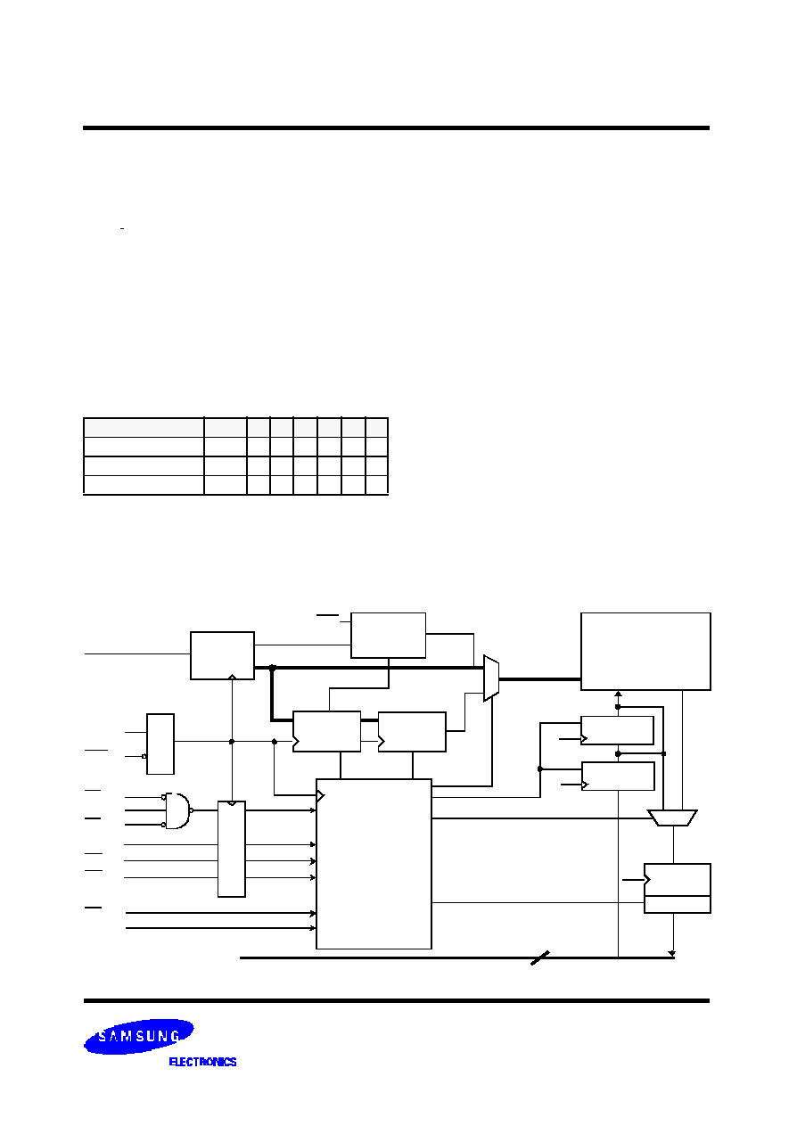
LOGIC BLOCK DIAGRAM
WE
BW
x
CLK
CKE
CS
1
CS
2
CS
2
ADV
OE
ZZ
DQa
0
~ DQd
7
or
DQa
0
~ DQb
8
ADDRESS
ADDRESS
REGISTER
C
O
N
T
R
O
L
L
O
G
I
C
A
0
~A
1
36/32 or 18
DQPa ~ DQPd
OUTPUT
BUFFER
REGISTER
DATA-IN
REGISTER
DATA-IN
REGISTER
K
K
K
REGISTER
BURST
ADDRESS
COUNTER
WRITE
ADDRESS
REGISTER
WRITE
CONTROL
LOGIC
C
O
N
T
R
O
L
R
E
G
I
S
T
E
R
K
A [0:18]or
A [0:19]
LBO
A
2
~A
18
or
A
2
~A
19
A
0
~A
1
(x=a,b,c,d or a,b)
512Kx36/32 , 1Mx18
MEMORY
ARRAY
K7N163245A
512Kx36/32 & 1Mx18 Pipelined NtRAM
TM
- 4 -
Rev 2.1
April 2003
K7N161845A
K7N163645A
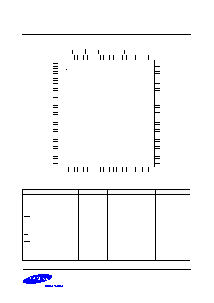
PIN CONFIGURATION
(TOP VIEW)
1
2
3
4
5
6
7
8
9
10
11
12
13
14
15
16
17
18
19
20
21
22
23
24
25
26
27
28
29
30
100 Pin TQFP
(20mm x 14mm)
DQPc
DQc
0
DQc
1
V
DDQ
V
SSQ
DQc
2
DQc
3
DQc
4
DQc
5
V
SSQ
V
DDQ
DQc
6
DQc
7
V
DD
V
DD
V
DD
V
SS
DQd
0
DQd
1
V
DDQ
V
SSQ
DQd
2
DQd
3
DQd
4
DQd
5
V
SSQ
V
DDQ
DQd
6
DQd
7
DQPd
80
79
78
77
76
75
74
73
72
71
70
69
68
67
66
65
64
63
62
61
60
59
58
57
56
55
54
53
52
51
DQPb
DQb
7
DQb
6
V
DDQ
V
SSQ
DQb
5
DQb
4
DQb
3
DQb
2
V
SSQ
V
DDQ
DQb
1
DQb
0
V
SS
V
DD
V
DD
ZZ
DQa
7
DQa
6
V
DDQ
V
SSQ
DQa
5
DQa
4
DQa
3
DQa
2
V
SSQ
V
DDQ
DQa
1
DQa
0
DQPa
1
0
0
9
9
9
8
9
7
9
6
9
5
9
4
9
3
9
2
9
1
9
0
8
9
8
8
8
7
8
6
8
5
8
4
8
3
8
2
A
6
A
7
C
S
1
C
S
2
B
W
d
B
W
c
B
W
b
B
W
a
C
S
2
V
D
D
V
S
S
C
L
K
W
E
C
K
E
O
E
A
D
V
A
1
8
A
1
7
A
8
8
1
A
9
5
0
4
9
4
8
4
7
4
6
4
5
4
4
4
3
4
2
4
1
4
0
3
9
3
8
3
7
3
6
3
5
3
4
3
3
3
2
A
1
6
A
1
5
A
1
4
A
1
3
A
1
2
A
1
1
A
1
0
N
.
C
.
N
.
C
.
V
D
D
V
S
S
N
.
C
.
N
.
C
.
A
0
A
1
A
2
A
3
A
4
A
5
3
1
L
B
O
1
2
3
4
5
6
7
8
9
10
11
12
13
14
15
16
17
18
19
20
21
22
23
24
25
26
27
28
29
30
NC/DQPc
DQc
0
DQc
1
V
DDQ
V
SSQ
DQc
2
DQc
3
DQc
4
DQc
5
V
SSQ
V
DDQ
DQc
6
DQc
7
V
DD
V
DD
V
DD
V
SS
DQd
0
DQd
1
V
DDQ
V
SSQ
DQd
2
DQd
3
DQd
4
DQd
5
V
SSQ
V
DDQ
DQd
6
DQd
7
NC/DQPd
80
79
78
77
76
75
74
73
72
71
70
69
68
67
66
65
64
63
62
61
60
59
58
57
56
55
54
53
52
51
DQPb/NC
DQb
7
DQb
6
V
DDQ
V
SSQ
DQb
5
DQb
4
DQb
3
DQb
2
V
SSQ
V
DDQ
DQb
1
DQb
0
V
SS
V
DD
V
DD
ZZ
DQa
7
DQa
6
V
DDQ
V
SSQ
DQa
5
DQa
4
DQa
3
DQa
2
V
SSQ
V
DDQ
DQa
1
DQa
0
DQPa/NC
1
0
0
9
9
9
8
9
7
9
6
9
5
9
4
9
3
9
2
9
1
9
0
8
9
8
8
8
7
8
6
8
5
8
4
8
3
8
2
A
6
A
7
C
S
1
C
S
2
B
W
d
B
W
c
B
W
b
B
W
a
C
S
2
V
D
D
V
S
S
C
L
K
W
E
C
K
E
O
E
A
D
V
A
1
8
A
1
7
A
8
8
1
A
9
5
0
4
9
4
8
4
7
4
6
4
5
4
4
4
3
4
2
4
1
4
0
3
9
3
8
3
7
3
6
3
5
3
4
3
3
3
2
A
1
6
A
1
5
A
1
4
A
1
3
A
1
2
A
1
1
A
1
0
N
.
C
.
N
.
C
.
V
D
D
V
S
S
N
.
C
.
N
.
C
.
A
0
A
1
A
2
A
3
A
4
A
5
3
1
L
B
O
PIN NAME
Note :
A
0
and A
1
are the two least significant bits(LSB) of the address field and set the internal burst counter if burst is desired.
SYMBOL
PIN NAME
TQFP PIN NO.
SYMBOL
PIN NAME
TQFP PIN NO.
A
0
- A
18
ADV
W E
CLK
CKE
CS
1
CS
2
CS
2
B Wx(x=a,b,c,d)
OE
ZZ
LBO
Address Inputs
Address Advance/Load
Read/Write Control Input
Clock
Clock Enable
Chip Select
Chip Select
Chip Select
Byte Write Inputs
Output Enable
Power Sleep Mode
Burst Mode Control
32,33,34,35,36,37,44
45,46,47,48,49,50,81
82,83,84,99,100
85
88
89
87
98
97
92
93,94,95,96
86
64
31
V
DD
V
SS
N.C.
DQa
0
~a
7
DQb
0
~b
7
DQc
0
~c
7
DQd
0
~d
7
DQPa~Pd
or NC
V
DDQ
V
SSQ
Power Supply
(2.5V)
Ground
No Connect
Data Inputs/Outputs
Data Inputs/Outputs
Data Inputs/Outputs
Data Inputs/Outputs
Data Inputs/Outputs
Output Power Supply
(2.5V)
Output Ground
14,15,16,41,65,66,91
17,40,67,90
38,39,42,43
52,53,56,57,58,59,62,63
68,69,72,73,74,75,78,79
2,3,6,7,8,9,12,13
18,19,22,23,24,25,28,29
51,80,1,30
4,11,20,27,54,61,70,77
5,10,21,26,55,60,71,76
K7N163645A(512Kx36)
K7N163245A(512Kx32)
K7N163245A
512Kx36/32 & 1Mx18 Pipelined NtRAM
TM
- 5 -
Rev 2.1
April 2003
K7N161845A
K7N163645A
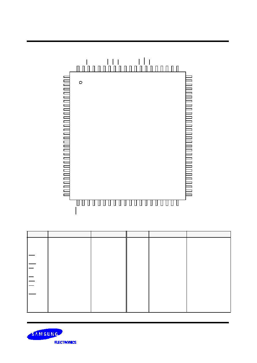
PIN CONFIGURATION
(TOP VIEW)
1
2
3
4
5
6
7
8
9
10
11
12
13
14
15
16
17
18
19
20
21
22
23
24
25
26
27
28
29
30
100 Pin TQFP
(20mm x 14mm)
N.C.
N.C.
N.C.
V
DDQ
V
SSQ
N.C.
N.C.
DQb
8
DQb
7
V
SSQ
V
DDQ
DQb
6
DQb
5
V
DD
V
DD
V
DD
V
SS
DQb
4
DQb
3
V
DDQ
V
SSQ
DQb
2
DQb
1
DQb
0
N.C.
V
SSQ
V
DDQ
N.C.
N.C.
N.C.
80
79
78
77
76
75
74
73
72
71
70
69
68
67
66
65
64
63
62
61
60
59
58
57
56
55
54
53
52
51
A
10
N.C.
N.C.
V
DDQ
V
SSQ
N.C.
DQa
0
DQa
1
DQa
2
V
SSQ
V
DDQ
DQa
3
DQa
4
V
SS
V
DD
V
DD
ZZ
DQa
5
DQa
6
V
DDQ
V
SSQ
DQa
7
DQa
8
N.C.
N.C.
V
SSQ
V
DDQ
N.C.
N.C.
N.C.
1
0
0
9
9
9
8
9
7
9
6
9
5
9
4
9
3
9
2
9
1
9
0
8
9
8
8
8
7
8
6
8
5
8
4
8
3
8
2
A
6
A
7
C
S
1
C
S
2
B
W
b
B
W
a
C
S
2
V
D
D
V
S
S
C
L
K
W
E
C
K
E
O
E
A
D
V
A
1
9
A
1
8
A
8
8
1
A
9
5
0
4
9
4
8
4
7
4
6
4
5
4
4
4
3
4
2
4
1
4
0
3
9
3
8
3
7
3
6
3
5
3
4
3
3
3
2
A
1
7
A
1
6
A
1
5
A
1
4
A
1
3
A
1
2
A
1
1
N
.
C
.
N
.
C
.
V
D
D
V
S
S
N
.
C
.
N
.
C
.
A
0
A
1
A
2
A
3
A
4
A
5
3
1
L
B
O
K7N161845A(1Mx18)
N
.
C
.
N
.
C
.
PIN NAME
Note :
A
0
and A
1
are the two least significant bits(LSB) of the address field and set the internal burst counter if burst is desired.
SYMBOL
PIN NAME
TQFP PIN NO.
SYMBOL
PIN NAME
TQFP PIN NO.
A
0
- A
19
ADV
WE
CLK
CKE
CS
1
CS
2
CS
2
BW x(x=a,b)
OE
ZZ
LBO
Address Inputs
Address Advance/Load
Read/Write Control Input
Clock
Clock Enable
Chip Select
Chip Select
Chip Select
Byte Write Inputs
Output Enable
Power Sleep Mode
Burst Mode Control
32,33,34,35,36,37,44
45,46,47,48,49,50,80,
81,82,83,84,99,100
85
88
89
87
98
97
92
93,94
86
64
31
V
DD
V
SS
N.C.
DQa
0
~a
8
DQb
0
~b
8
V
DDQ
V
SSQ
Power Supply
(2.5V)
Ground
No Connect
Data Inputs/Outputs
Data Inputs/Outputs
Output Power Supply
(2.5V)
Output Ground
14,15,16,41,65,66,91
17,40,67,90
1,2,3,6,7,25,28,29,30,
38,39,42,43,51,52,53,
56,57,75,78,79,95,96
58,59,62,63,68,69,72,73,74
8,9,12,13,18,19,22,23,24
4,11,20,27,54,61,70,77
5,10,21,26,55,60,71,76

K7N163245A
512Kx36/32 & 1Mx18 Pipelined NtRAM
TM
- 6 -
Rev 2.1
April 2003
K7N161845A
K7N163645A
165-PIN FBGA PACKAGE CONFIGURATIONS
(TOP VIEW)
PIN NAME
SYMBOL
PIN NAME
SYMBOL
PIN NAME
A
A
0
,A
1
ADV
WE
CLK
CKE
CS
1
CS
2
CS
2
BWx
(x=a,b,c,d)
OE
ZZ
LBO
TCK
TMS
TDI
TDO
Address Inputs
Burst Address Inputs
Address Advance/Load
Read/Write Control Input
Clock
Clock Enable
Chip Select
Chip Select
Chip Select
Byte Write Inputs
Output Enable
Power Sleep Mode
Burst Mode Control
JTAG Test Clock
JTAG Test Mode Select
JTAG Test Data Input
JTAG Test Data Output
V
DD
V
SS
N.C.
DQa
DQb
DQc
DQd
DQPa~Pd
V
DDQ
Power Supply
Ground
No Connect
Data Inputs/Outputs
Data Inputs/Outputs
Data Inputs/Outputs
Data Inputs/Outputs
Data Inputs/Outputs
Output Power Supply
K7N163645A(512Kx36)
Note :
* A
0
and A
1
are the two least significant bits(LSB) of the address field and set the internal burst counter if burst is desired.
1
2
3
4
5
6
7
8
9
10
11
A
NC
A
CS 1
BW c
BWb
CS2
CKE
ADV
A
A
NC
B
NC
A
CS2
BWd
BWa
CLK
WE
OE
A
A
NC
C
DQPc
NC
V
DDQ
V
SS
V
SS
V
SS
V
SS
V
SS
V
DDQ
NC
DQPb
D
DQc
DQc
V
DDQ
V
DD
V
SS
V
SS
V
SS
V
DD
V
DDQ
DQb
DQb
E
DQc
DQc
V
DDQ
V
DD
V
SS
V
SS
V
SS
V
DD
V
DDQ
DQb
DQb
F
DQc
DQc
V
DDQ
V
DD
V
SS
V
SS
V
SS
V
DD
V
DDQ
DQb
DQb
G
DQc
DQc
V
DDQ
V
DD
V
SS
V
SS
V
SS
V
DD
V
DDQ
DQb
DQb
H
NC
V
DD
NC
V
DD
V
SS
V
SS
V
SS
V
DD
NC
NC
ZZ
J
DQd
DQd
V
DDQ
V
DD
V
SS
V
SS
V
SS
V
DD
V
DDQ
DQa
DQa
K
DQd
DQd
V
DDQ
V
DD
V
SS
V
SS
V
SS
V
DD
V
DDQ
DQa
DQa
L
DQd
DQd
V
DDQ
V
DD
V
SS
V
SS
V
SS
V
DD
V
DDQ
DQa
DQa
M
DQd
DQd
V
DDQ
V
DD
V
SS
V
SS
V
SS
V
DD
V
DDQ
DQa
DQa
N
DQPd
NC
V
DDQ
V
SS
NC
NC
NC
V
SS
V
DDQ
NC
DQPa
P
NC
NC
A
A
TDI
A
1
*
TDO
A
A
A
NC
R
LBO
NC
A
A
TMS
A
0
*
TCK
A
A
A
A

K7N163245A
512Kx36/32 & 1Mx18 Pipelined NtRAM
TM
- 7 -
Rev 2.1
April 2003
K7N161845A
K7N163645A
PIN NAME
SYMBOL
PIN NAME
SYMBOL
PIN NAME
A
A
0
,A
1
ADV
WE
CLK
CKE
CS
1
CS
2
CS
2
BWx
(x=a,b)
OE
ZZ
LBO
TCK
TMS
TDI
TDO
Address Inputs
Burst Address Inputs
Address Advance/Load
Read/Write Control Input
Clock
Clock Enable
Chip Select
Chip Select
Chip Select
Byte Write Inputs
Output Enable
Power Sleep Mode
Burst Mode Control
JTAG Test Clock
JTAG Test Mode Select
JTAG Test Data Input
JTAG Test Data Output
V
DD
V
SS
N.C.
DQa
DQb
DQPa, Pb
V
DDQ
Power Supply
Ground
No Connect
Data Inputs/Outputs
Data Inputs/Outputs
Data Inputs/Outputs
Output Power Supply
165-PIN FBGA PACKAGE CONFIGURATIONS
(TOP VIEW)
K7N161845A(1Mx18)
Note :
* A
0
and A
1
are the two least significant bits(LSB) of the address field and set the internal burst counter if burst is desired.
1
2
3
4
5
6
7
8
9
10
11
A
NC
A
CS 1
BWb
NC
CS2
CKE
ADV
A
A
A
B
NC
A
CS2
NC
BWa
CLK
WE
OE
A
A
NC
C
NC
NC
V
DDQ
V
SS
V
SS
V
SS
V
SS
V
SS
V
DDQ
NC
DQPa
D
NC
DQb
V
DDQ
V
DD
V
SS
V
SS
V
SS
V
DD
V
DDQ
NC
DQa
E
NC
DQb
V
DDQ
V
DD
V
SS
V
SS
V
SS
V
DD
V
DDQ
NC
DQa
F
NC
DQb
V
DDQ
V
DD
V
SS
V
SS
V
SS
V
DD
V
DDQ
NC
DQa
G
NC
DQb
V
DDQ
V
DD
V
SS
V
SS
V
SS
V
DD
V
DDQ
NC
DQa
H
NC
V
DD
NC
V
DD
V
SS
V
SS
V
SS
V
DD
NC
NC
ZZ
J
DQb
NC
V
DDQ
V
DD
V
SS
V
SS
V
SS
V
DD
V
DDQ
DQa
NC
K
DQb
NC
V
DDQ
V
DD
V
SS
V
SS
V
SS
V
DD
V
DDQ
DQa
NC
L
DQb
NC
V
DDQ
V
DD
V
SS
V
SS
V
SS
V
DD
V
DDQ
DQa
NC
M
DQb
NC
V
DDQ
V
DD
V
SS
V
SS
V
SS
V
DD
V
DDQ
DQa
NC
N
DQPb
NC
V
DDQ
V
SS
NC
NC
NC
V
SS
V
DDQ
NC
NC
P
NC
NC
A
A
TDI
A
1
*
TDO
A
A
A
NC
R
LBO
NC
A
A
TMS
A
0
*
TCK
A
A
A
A
K7N163245A
512Kx36/32 & 1Mx18 Pipelined NtRAM
TM
- 8 -
Rev 2.1
April 2003
K7N161845A
K7N163645A
119BGA PACKAGE PIN CONFIGURATIONS
(TOP VIEW)
Only for K7N163645A - HC16 (512Kx36)
Note :
* A
0
and A
1
are the two least significant bits(LSB) of the address field and set the internal burst counter if burst is desired.
1
2
3
4
5
6
7
A
V
DDQ
A
A
A
A
A
V
DDQ
B
NC
CS
2
A
ADV
A
CS
2
NC
C
NC
A
A
V
DD
A
A
NC
D
DQc
DQPc
V
SS
NC
V
SS
DQPb
DQb
E
DQc
DQc
V
SS
CS
1
V
SS
DQb
DQb
F
V
DDQ
DQc
V
SS
OE
V
SS
DQb
V
DDQ
G
DQc
DQc
BWc
A
BWb
DQb
DQb
H
DQc
DQc
V
SS
WE
V
SS
DQb
DQb
J
V
DDQ
V
DD
NC
V
DD
NC
V
DD
V
DDQ
K
DQd
DQd
V
SS
CLK
V
SS
DQa
DQa
L
DQd
DQd
BW d
NC
BWa
DQa
DQa
M
V
DDQ
DQd
V
SS
CKE
V
SS
DQa
V
DDQ
N
DQd
DQd
V
SS
A
1
*
V
SS
DQa
DQa
P
DQd
DQPd
V
SS
A
0
*
V
SS
DQPa
DQa
R
NC
A
LBO
V
DD
NC
A
NC
T
NC
NC
A
A
A
NC
ZZ
U
V
DDQ
TMS
TDI
TCK
TDO
NC
V
DDQ
PIN NAME
SYMBOL
PIN NAME
SYMBOL
PIN NAME
A
A
0
,A
1
ADV
WE
CLK
CKE
CS
1
CS
2
CS
2
BWx
(x=a,b,c,d)
OE
ZZ
LBO
TCK
TMS
TDI
TDO
Address Inputs
Burst Address Inputs
Address Advance/Load
Read/Write Control Input
Clock
Clock Enable
Chip Select
Chip Select
Chip Select
Byte Write Inputs
Output Enable
Power Sleep Mode
Burst Mode Control
JTAG Test Clock
JTAG Test Mode Select
JTAG Test Data Input
JTAG Test Data Output
V
DD
V
SS
N.C.
DQa
DQb
DQc
DQd
DQPa~Pd
V
DDQ
Power Supply
Ground
No Connect
Data Inputs/Outputs
Data Inputs/Outputs
Data Inputs/Outputs
Data Inputs/Outputs
Data Inputs/Outputs
Output Power Supply

K7N163245A
512Kx36/32 & 1Mx18 Pipelined NtRAM
TM
- 9 -
Rev 2.1
April 2003
K7N161845A
K7N163645A
119BGA PACKAGE PIN CONFIGURATIONS
(TOP VIEW)
Only for
K7N161845A - HC13 (1Mx18)
Note :
* A
0
and A
1
are the two least significant bits(LSB) of the address field and set the internal burst counter if burst is desired.
1
2
3
4
5
6
7
A
V
DDQ
A
A
A
A
A
V
DDQ
B
NC
CS
2
A
ADV
A
CS
2
NC
C
NC
A
A
V
DD
A
A
NC
D
DQb
NC
V
SS
NC
V
SS
DQPa
NC
E
NC
DQb
V
SS
CS
1
V
SS
NC
DQa
F
V
DDQ
NC
V
SS
OE
V
SS
DQa
V
DDQ
G
NC
DQb
BW b
A
V
SS
NC
DQa
H
DQb
NC
V
SS
WE
V
SS
DQa
NC
J
V
DDQ
V
DD
NC
V
DD
NC
V
DD
V
DDQ
K
NC
DQb
V
SS
CLK
V
SS
NC
DQa
L
DQb
NC
V
SS
NC
BWa
DQa
NC
M
V
DDQ
DQb
V
SS
CKE
V
SS
NC
V
DDQ
N
DQb
NC
V
SS
A
1
*
V
SS
DQa
NC
P
NC
DQPb
V
SS
A
0
*
V
SS
NC
DQa
R
NC
A
LBO
V
DD
NC
A
NC
T
NC
A
A
NC
A
A
ZZ
U
V
DDQ
TMS
TDI
TCK
TDO
NC
V
DDQ
PIN NAME
SYMBOL
PIN NAME
SYMBOL
PIN NAME
A
A
0
,A
1
ADV
WE
CLK
CKE
CS
1
CS
2
CS
2
BWx
(x=a,b)
OE
ZZ
LBO
TCK
TMS
TDI
TDO
Address Inputs
Burst Address Inputs
Address Advance/Load
Read/Write Control Input
Clock
Clock Enable
Chip Select
Chip Select
Chip Select
Byte Write Inputs
Output Enable
Power Sleep Mode
Burst Mode Control
JTAG Test Clock
JTAG Test Mode Select
JTAG Test Data Input
JTAG Test Data Output
V
DD
V
SS
N.C.
DQa
DQb
DQPa, Pb
V
DDQ
Power Supply
Ground
No Connect
Data Inputs/Outputs
Data Inputs/Outputs
Data Inputs/Outputs
Output Power Supply
K7N163245A
512Kx36/32 & 1Mx18 Pipelined NtRAM
TM
- 10 -
Rev 2.1
April 2003
K7N161845A
K7N163645A
FUNCTION DESCRIPTION
The K7N163645A, K7N163245A and K7N161845A are NtRAM
TM
designed to sustain 100% bus bandwidth by eliminating turnaround
cycle when there is transition from Read to Write, or vice versa.
All inputs (with the exception of OE, LBO and ZZ) are synchronized to rising clock edges.
All read, write and deselect cycles are initiated by the ADV input. Subsequent burst addresses can be internally generated by the
burst advance pin (ADV). ADV should be driven to Low once the device has been deselected in order to load a new address for next
operation.
Clock Enable(CKE) pin allows the operation of the chip to be suspended as long as necessary. When CKE is high, all synchronous
inputs are ignored and the internal device registers will hold their previous values.
NtRAM
TM
latches external address and initiates a cycle, when CKE, ADV are driven to low and all three chip enables( CS
1
, CS
2
, CS
2
)
are active .
Output Enable(OE) can be used to disable the output at any given time.
Read operation is initiated when at the rising edge of the clock, the address presented to the address inputs are latched in the
address register, CKE is driven low, all three chip enables(CS
1
, CS
2
, CS
2
) are active, the write enable input signals WE are driven
high, and ADV driven low.The internal array is read between the first rising edge and the second rising edge of the clock and the data
is latched in the output register. At the second clock edge the data is driven out of the SRAM. Also during read operation OE must
be driven low for the device to drive out the requested data.
Write operation occurs when WE is driven low at the rising edge of the clock. B W[d:a] can be used for byte write operation. The pipe-
lined NtRAM
TM
uses a late-late write cycle to utilize 100% of the bandwidth.
At the first rising edge of the clock, W E and address are registered, and the data associated with that address is required two cycle
later.
Subsequent addresses are generated by ADV High for the burst access as shown below. The starting point of the burst seguence is
provided by the external address. The burst address counter wraps around to its initial state upon completion.
The burst sequence is determined by the state of the LBO pin. When this pin is low, linear burst sequence is selected.
And when this pin is high, Interleaved burst sequence is selected.
During normal operation, ZZ must be driven low. When ZZ is driven high, the SRAM will enter a Power Sleep Mode after 2 cycles. At
this time, internal state of the SRAM is preserved. When ZZ returns to low, the SRAM normally operates after 2 cycles of wake up
time.
BURST SEQUENCE TABLE
(Interleaved Burst, LBO=High)
LBO PIN
HIGH
Case 1
Case 2
Case 3
Case 4
A
1
A
0
A
1
A
0
A
1
A
0
A
1
A
0
First Address
Fourth Address
0
0
1
1
0
1
0
1
0
0
1
1
1
0
1
0
1
1
0
0
0
1
0
1
1
1
0
0
1
0
1
0
BQ TABLE
(Linear Burst, LBO=Low)
Note :
1. LBO pin must be tied to High or Low, and Floating State must not be allowed
.
LBO PIN
LOW
Case 1
Case 2
Case 3
Case 4
A
1
A
0
A
1
A
0
A
1
A
0
A
1
A
0
First Address
Fourth Address
0
0
1
1
0
1
0
1
0
1
1
0
1
0
1
0
1
1
0
0
0
1
0
1
1
0
0
1
1
0
1
0

K7N163245A
512Kx36/32 & 1Mx18 Pipelined NtRAM
TM
- 11 -
Rev 2.1
April 2003
K7N161845A
K7N163645A
STATE DIAGRAM FOR NtRAM
TM
BEGIN
WRITE
BURST
WRITE
BEGIN
READ
WRITE
DS
REA
D
BURST
READ
DS
WR
ITE
DS
READ
DS
RE
AD
D
S
W
RI
TE
B
U
R
S
T
DESELECT
B
U
R
S
T
R
EA
D
B
U
R
S
T
W
R
IT
E
READ
WRITE
BURST
BURST
Notes :
1. An IGNORE CLOCK EDGE cycle is not shown is the above diagram. This is because CKE HIGH only blocks the clock(CLK) input and does
not change the state of the device.
2. States change on the rising edge of the clock(CLK)
COMMAND
ACTION
DS
DESELECT
READ
BEGIN READ
WRITE
BEGIN WRITE
BURST
BEGIN READ
BEGIN WRITE
CONTINUE DESELECT
K7N163245A
512Kx36/32 & 1Mx18 Pipelined NtRAM
TM
- 12 -
Rev 2.1
April 2003
K7N161845A
K7N163645A
SYNCHRONOUS TRUTH TABLE
Notes
: 1. X means "Don
t Care". 2. The rising edge of clock is symbolized by (
).
3. A continue deselect cycle can only be enterd if a deselect cycle is executed first.
4. WRITE = L means Write operation in WRITE TRUTH TABLE.
WRITE = H means Read operation in WRITE TRUTH TABLE.
5. Operation finally depends on status of asynchronous input pins(ZZ and OE).
CS
1
CS
2
CS
2
ADV
WE
BW x
OE
CKE
CLK
ADDRESS ACCESSED
OPERATION
H
X
X
L
X
X
X
L
N/A
Not Selected
X
L
X
L
X
X
X
L
N/A
Not Selected
X
X
H
L
X
X
X
L
N/A
Not Selected
X
X
X
H
X
X
X
L
N/A
Not Selected Continue
L
H
L
L
H
X
L
L
External Address
Begin Burst Read Cycle
X
X
X
H
X
X
L
L
Next Address
Continue Burst Read Cycle
L
H
L
L
H
X
H
L
External Address
NOP/Dummy Read
X
X
X
H
X
X
H
L
Next Address
Dummy Read
L
H
L
L
L
L
X
L
External Address
Begin Burst Write Cycle
X
X
X
H
X
L
X
L
Next Address
Continue Burst Write Cycle
L
H
L
L
L
H
X
L
N/A
NOP/Write Abort
X
X
X
H
X
H
X
L
Next Address
Write Abort
X
X
X
X
X
X
X
H
Current Address
Ignore Clock
WRITE TRUTH TABLE
(x36 / x32)
Notes
: 1. X means "Don
t Care".
2. All inputs in this table must meet setup and hold time around the rising edge of CLK(
).
WE
BW a
BW b
BWc
BW d
OPERATION
H
X
X
X
X
READ
L
L
H
H
H
WRITE BYTE a
L
H
L
H
H
WRITE BYTE b
L
H
H
L
H
WRITE BYTE c
L
H
H
H
L
WRITE BYTE d
L
L
L
L
L
WRITE ALL BYTEs
L
H
H
H
H
WRITE ABORT/NOP
TRUTH TABLES
WRITE TRUTH TABLE
(x18)
Notes
: 1. X means "Don
t Care".
2. All inputs in this table must meet setup and hold time around the rising edge of CLK(
).
WE
BWa
BW b
OPERATION
H
X
X
READ
L
L
H
WRITE BYTE a
L
H
L
WRITE BYTE b
L
L
L
WRITE ALL BYTEs
L
H
H
WRITE ABORT/NOP
K7N163245A
512Kx36/32 & 1Mx18 Pipelined NtRAM
TM
- 13 -
Rev 2.1
April 2003
K7N161845A
K7N163645A
ASYNCHRONOUS TRUTH TABLE
OPERATION
ZZ
OE
I/O STATUS
Sleep Mode
H
X
High-Z
Read
L
L
DQ
L
H
High-Z
Write
L
X
Din, High-Z
Deselected
L
X
High-Z
Notes
1. X means "Don
t Care".
2. Sleep Mode means power Sleep Mode of which stand-by current does
not depend on cycle time.
3. Deselected means power Sleep Mode of which stand-by current
depends on cycle time.
ABSOLUTE MAXIMUM RATINGS*
*Note
: Stresses greater than those listed under "Absolute Maximum Ratings" may cause permanent damage to the device. This is a stress rating only
and functional operation of the device at these or any other conditions above those indicated in the operating sections of this specification is not
implied. Exposure to absolute maximum rating conditions for extended periods may affect reliability.
PARAMETER
SYMBOL
RATING
UNIT
Voltage on V
DD
Supply Relative to V
SS
V
DD
-0.3 to 3.6
V
Voltage on Any Other Pin Relative to V
SS
V
IN
-0.3 to V
DD
+0.3
V
Power Dissipation
P
D
1.6
W
Storage Temperature
T
STG
-65 to 150
∞
C
Operating Temperature
Commercial
T
OPR
0 to 70
∞
C
Industrial
T
OPR
-40 to 85
∞
C
Storage Temperature Range Under Bias
T
BIAS
-10 to 85
∞
C
OPERATING CONDITIONS
(0
∞
C
T
A
70
∞
C)
*Note
: V
DD
and V
DDQ
must be supplied with identical vlotage levels
.
The above parameters are also guaranteed at industrial temperature range.
PARAMETER
SYMBOL
MIN
Typ.
MAX
UNIT
Supply Voltage
V
DD
2.375
2.5
2.625
V
V
DDQ
2.375
2.5
2.625
V
Ground
V
SS
0
0
0
V
CAPACITANCE*
(T
A
=25
∞
C, f=1MHz)
*Note
: Sampled not 100% tested.
PARAMETER
SYMBOL
TEST CONDITION
MIN
MAX
UNIT
Input Capacitance
C
IN
V
IN
=0V
-
5
pF
Output Capacitance
C
OUT
V
OUT
=0V
-
7
pF

K7N163245A
512Kx36/32 & 1Mx18 Pipelined NtRAM
TM
- 14 -
Rev 2.1
April 2003
K7N161845A
K7N163645A
DC ELECTRICAL CHARACTERISTICS
(V
DD
=2.5V
±
5%, T
A
=0
∞
C to +70
∞
C)
Notes :
1. The above parameters are also guaranteed at industrial temperature range.
2. Reference AC Operating Conditions and Characteristics for input and timing.
3. Data states are all zero.
4. In Case of I/O Pins, the Max. V
IH
=V
DDQ
+0.3V
PARAMETER
SYMBOL
TEST CONDITIONS
MIN
MAX
UNIT
NOTES
Input Leakage Current(except ZZ)
I
IL
V
DD
=Max ; V
IN
=V
SS
to V
DD
-2
+2
µ
A
Output Leakage Current
I
OL
Output Disabled,
-2
+2
µ
A
Operating Current
I
CC
V
DD
=Max I
OUT
=0mA
Cycle Time
t
CYC
Min
-25
-
470
mA
1,2
-22
-
430
-20
-
400
-16
-
350
-13
-
290
Standby Current
I
SB
Device deselected, I
OUT
=0mA,
ZZ
V
IL
, f=Max,
All Inputs
0.2V or
V
DD
-0.2V
-25
-
120
mA
-22
-
110
-20
-
100
-16
-
90
-13
-
90
I
SB1
Device deselected, I
OUT
=0mA, ZZ
0.2V, f=0,
All Inputs=fixed (V
DD
-0.2V or 0.2V)
-
70
mA
I
SB2
Device deselected, I
OUT
=0mA, ZZ
V
DD
-0.2V,
f=Max, All Inputs
V
IL
or
V
IH
-
60
mA
Output Low Voltage
V
OL
I
OL
=1.0mA
-
0.4
V
Output High Voltage
V
OH
I
OH
=-1.0mA
2.0
-
V
Input Low Voltage
V
IL
-0.3*
0.7
V
Input High Voltage
V
IH
1.7
V
DD
+0.3**
V
3
(T
A
=0 to 70
∞
C, V
DD
=2.5V
±
5%, unless otherwise specified)
TEST CONDITIONS
* The above parameters are also guaranteed at industrial temperature range.
PARAMETER
VALUE
Input Pulse Level
0 to 2.5V
Input Rise and Fall Time(Measured at 20% to 80%)
1.0V/ns
Input and Output Timing Reference Levels
V
DDQ
/2
Output Load
See Fig. 1
V
SS
V
IH
V
SS-
0.8V
20% t
CYC
(MIN)
K7N163245A
512Kx36/32 & 1Mx18 Pipelined NtRAM
TM
- 15 -
Rev 2.1
April 2003
K7N161845A
K7N163645A
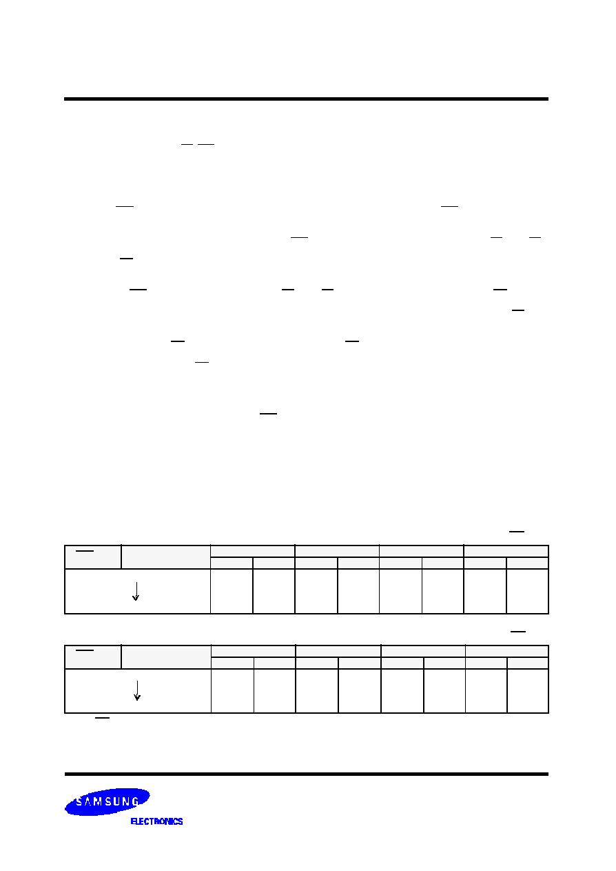
AC TIMING CHARACTERISTICS
Notes
: 1. The above parameters are also guaranteed at industrial temperature range.
2. All address inputs must meet the specified setup and hold times for all rising clock(CLK) edges when ADV is sampled low and CS is sampled
low. All other synchronous inputs must meet the specified setup and hold times whenever this device is chip selected.
3. Chip selects must be valid at each rising edge of CLK(when ADV is Low) to remain enabled.
4. A write cycle is defined by WE low having been registered into the device at ADV Low, A Read cycle is defined by WE High with ADV Low,
Both cases must meet setup and hold times.
5. To avoid bus contention, At a given voltage and temperature t
LZC
is more than t
HZC.
The specs as shown do not imply bus contention because t
LZC
is a Min. parameter that is worst case at totally different test conditions
(0
∞
C,2.625V) than t
HZC
, which is a Max. parameter(worst case at 70
∞
C,2.375V)
It is not possible for two SRAMs on the same board to be at such different voltage and temperature.
PARAMETER
SYMBOL
-25
-22
-20
-16
-13
UNIT
MIN
MAX MIN MAX MIN MAX MIN MAX MIN
MAX
Cycle Time
t
CYC
4.0
-
4.4
-
5.0
-
6.0
-
7.5
-
ns
Clock Access Time
t
CD
-
2.6
-
2.8
-
3.2
-
3.5
-
4.2
ns
Output Enable to Data Valid
t
OE
-
2.6
-
2.8
-
3.2
-
3.5
-
4.2
ns
Clock High to Output Low-Z
t
LZC
1.5
-
1.5
-
1.5
-
1.5
-
1.5
-
ns
Output Hold from Clock High
t
OH
1.5
-
1.5
-
1.5
-
1.5
-
1.5
-
ns
Output Enable Low to Output Low-Z
t
LZOE
0
-
0
-
0
-
0
-
0
-
ns
Output Enable High to Output High-Z
t
HZOE
-
2.6
-
2.8
-
3.0
-
3.0
-
3.5
ns
Clock High to Output High-Z
t
HZC
-
2.6
-
2.8
-
3.0
-
3.0
-
3.5
ns
Clock High Pulse Width
t
CH
1.7
-
2.0
-
2.0
-
2.2
-
3.0
-
ns
Clock Low Pulse Width
t
CL
1.7
-
2.0
-
2.0
-
2.2
-
3.0
-
ns
Address Setup to Clock High
t
AS
1.2
-
1.4
-
1.4
-
1.5
-
1.5
-
ns
CKE Setup to Clock High
t
CES
1.2
-
1.4
-
1.4
-
1.5
-
1.5
-
ns
Data Setup to Clock High
t
DS
1.2
-
1.4
-
1.4
-
1.5
-
1.5
-
ns
Write Setup to Clock High (WE, BW
X
)
t
WS
1.2
-
1.4
-
1.4
-
1.5
-
1.5
-
ns
Address Advance Setup to Clock High
t
ADVS
1.2
-
1.4
-
1.4
-
1.5
-
1.5
-
ns
Chip Select Setup to Clock High
t
CSS
1.2
-
1.4
-
1.4
-
1.5
-
1.5
-
ns
Address Hold from Clock High
t
AH
0.3
-
0.4
-
0.4
-
0.5
-
0.5
-
ns
CKE Hold from Clock High
t
CEH
0.3
-
0.4
-
0.4
-
0.5
-
0.5
-
ns
Data Hold from Clock High
t
DH
0.3
-
0.4
-
0.4
-
0.5
-
0.5
-
ns
Write Hold from Clock High (WE , BW
X
)
t
WH
0.3
-
0.4
-
0.4
-
0.5
-
0.5
-
ns
Address Advance Hold from Clock High
t
ADVH
0.3
-
0.4
-
0.4
-
0.5
-
0.5
-
ns
Chip Select Hold from Clock High
t
CSH
0.3
-
0.4
-
0.4
-
0.5
-
0.5
-
ns
ZZ High to Power Down
t
PDS
2
-
2
-
2
-
2
-
2
-
cycle
ZZ Low to Power Up
t
PUS
2
-
2
-
2
-
2
-
2
-
cycle
(V
DD
=2.5V
±
5%, T
A
=0 to 70
∞
C)
Output Load(B),
(for t
LZC
, t
LZOE
, t
HZOE
& t
HZC
)
Dout
1538
5pF*
+2.5V
1667
Fig. 1
* Including Scope and Jig Capacitance
Output Load(A)
Dout
Zo=50
RL=50
VL=V
DDQ
/2
30pF*
K7N163245A
512Kx36/32 & 1Mx18 Pipelined NtRAM
TM
- 16 -
Rev 2.1
April 2003
K7N161845A
K7N163645A
SLEEP MODE
SLEEP MODE is a low current, power-down mode in which the device is deselected and current is reduced to I
SB2
. The duration of
SLEEP MODE is dictated by the length of time the ZZ is in a High state.
After entering SLEEP MODE, all inputs except ZZ become disabled and all outputs go to High-Z
The ZZ pin is an asynchronous, active high input that causes the device to enter SLEEP MODE.
When the ZZ pin becomes a logic High, I
SB2
is guaranteed after the time t
ZZI
is met. Any operation pending when entering SLEEP
MODE is not guaranteed to successful complete. Therefore, SLEEP MODE (READ or WRITE) must not be initiated until valid pend-
ing operations are completed. similarly, when exiting SLEEP MODE during t
PUS
, only a DESELECT or READ cycle should be given
while the SRAM is transitioning out of SLEEP MODE.
SLEEP MODE ELECTRICAL CHARACTERISTICS
DESCRIPTION
CONDITIONS
SYMBOL
MIN
MAX
UNITS
Current during SLEEP MODE
ZZ
V
IH
I
SB2
60
mA
ZZ active to input ignored
t
PDS
2
cycle
ZZ inactive to input sampled
t
PUS
2
cycle
ZZ active to SLEEP current
t
ZZI
2
cycle
ZZ inactive to exit SLEEP current
t
RZZI
0
K
t
PDS
ZZ setup cycle
t
RZZI
ZZ
Isupply
All inputs
(except ZZ)
Outputs
(Q)
t
ZZI
t
PUS
ZZ recovery cycle
Deselect or Read Only
High-Z
DON
T CARE
I
SB2
SLEEP MODE WAVEFORM
Normal
operation
cycle
Deselect or Read Only

K7N163245A
512Kx36/32 & 1Mx18 Pipelined NtRAM
TM
- 17 -
Rev 2.1
April 2003
K7N161845A
K7N163645A
IEEE 1149.1 TEST ACCESS PORT AND BOUNDARY SCAN-JTAG
This part contains an IEEE standard 1149.1 Compatible Test Access Port(TAP). The package pads are monitored by the Serial Scan
circuitry when in test mode. This is to support connectivity testing during manufacturing and system diagnostics. Internal data is not
driven out of the SRAM under JTAG control. In conformance with IEEE 1149.1, the SRAM contains a TAP controller, Instruction Reg-
ister, Bypass Register and ID register. The TAP controller has a standard 16-state machine that resets internally upon power-up,
therefore, TRST signal is not required. It is possible to use this device without utilizing the TAP. To disable the TAP controller without
interfacing with normal operation of the SRAM, TCK must be tied to V
SS
to preclude mid level input. TMS and TDI are designed so an
undriven input will produce a response identical to the application of a logic 1, and may be left unconnected. But they may also be
tied to V
DD
through a resistor. TDO should be left unconnected.
TAP Controller State Diagram
JTAG Block Diagram
SRAM
CORE
BYPASS Reg.
Identification Reg.
Instruction Reg.
Control Signals
TAP Controller
TDO
TDI
TMS
TCK
Test Logic Reset
Run Test Idle
0
1
1
1
1
0
0
0
1
0
1
1
0
0
0
1
0
1
1
1
0
0
0
0
0
0
0
Select DR
Capture DR
Shift DR
Exit1 DR
Pause DR
Exit2 DR
Update DR
Select IR
Capture IR
Shift IR
Exit1 IR
Pause IR
Exit2 IR
Update IR
1
1
1
1
1
JTAG Instruction Coding
NOTE
:
1. Places DQs in Hi-Z in order to sample all input data regardless of other
SRAM inputs. This instruction is not IEEE 1149.1 compliant.
2. Places DQs in Hi-Z in order to sample all input data regardless of other
SRAM inputs.
3. TDI is sampled as an input to the first ID register to allow for the serial shift
of the external TDI data.
4. Bypass register is initiated to V
SS
when BYPASS instruction is invoked. The
Bypass Register also holds serially loaded TDI when exiting the Shift DR
states.
5. SAMPLE instruction dose not places DQs in Hi-Z.
6. This instruction is reserved for future use.
IR2 IR1 IR0
Instruction
TDO Output
Notes
0
0
0 EXTEST
Boundary Scan Register
1
0
0
1 IDCODE
Identification Register
3
0
1
0 SAMPLE-Z
Boundary Scan Register
2
0
1
1 BYPASS
Bypass Register
4
1
0
0 SAMPLE
Boundary Scan Register
5
1
0
1 RESERVED Do Not Use
6
1
1
0 BYPASS
Bypass Register
4
1
1
1 BYPASS
Bypass Register
4

K7N163245A
512Kx36/32 & 1Mx18 Pipelined NtRAM
TM
- 18 -
Rev 2.1
April 2003
K7N161845A
K7N163645A
ID REGISTER DEFINITION
Part
Revision Number
(31:28)
Part Configuration
(27:18)
Vendor Definition
(17:12)
Samsung JEDEC Code
(11: 1)
Start Bit(0)
512Kx36
0000
00111 00100
XXXXXX
00001001110
1
1Mx18
0000
01000 00011
XXXXXX
00001001110
1
SCAN REGISTER DEFINITION
Part
Instruction Register
Bypass Register
ID Register
Boundary Scan
512Kx36
3 bits
1 bits
32 bits
75 bits
1Mx18
3 bits
1 bits
32 bits
75 bits
165FBGA BOUNDARY SCAN EXIT ORDER(x36)
1
1R
LBO
CLK
6B
39
2
6N
NC
NC
11B
40
3
11P
NC
NC
1A
41
4
8P
A
CS2
6A
42
5
8R
A
BWa
5B
43
6
9R
A
BWb
5A
44
7
9P
A
BWc
4A
45
8
10P
A
BWd
4B
46
9
10R
A
CS2
3B
47
10
11R
A
CS1
3A
48
11
11H
ZZ
A
2A
49
12
11N
DQa
A
2B
50
13
11M
DQa
NC
1B
51
14
11L
DQa
DQc
1C
52
15
11K
DQa
DQc
1D
53
16
11J
DQa
DQc
1E
54
17
10M
DQa
DQc
1F
55
18
10L
DQa
DQc
1G
56
19
10K
DQa
DQc
2D
57
20
10J
DQa
DQc
2E
58
21
11G
DQb
DQc
2F
59
22
11F
DQb
DQc
2G
60
23
11E
DQb
DQd
1J
61
24
11D
DQb
DQd
1K
62
25
10G
DQb
DQd
1L
63
26
10F
DQb
DQd
1M
64
27
10E
DQb
DQd
2J
65
28
10D
DQb
DQd
2K
66
29
11C
DQb
DQd
2L
67
30
11A
NC
DQd
2M
68
31
10A
A
DQd
1N
69
32
10B
A
A
3P
70
33
9A
A
A
3R
71
34
9B
A
A
4R
72
35
8A
ADV
A
4P
73
36
8B
OE
A1
6P
74
37
7A
CKE
A0
6R
75
38
7B
WE
165FBGA BOUNDARY SCAN EXIT ORDER(x18
)
1
1R
LBO
CLK
6B
39
2
6N
NC
NC
11B
40
3
11P
NC
NC
1A
41
4
8P
A
CS2
6A
42
5
8R
A
BW a
5B
43
6
9R
A
NC
5A
44
7
9P
A
BW b
4A
45
8
10P
A
NC
4B
46
9
10R
A
CS2
3B
47
10
11R
A
CS1
3A
48
11
11H
ZZ
A
2A
49
12
11N
NC
A
2B
50
13
11M
NC
NC
1B
51
14
11L
NC
NC
1C
52
15
11K
NC
NC
1D
53
16
11J
NC
NC
1E
54
17
10M
DQa
NC
1F
55
18
10L
DQa
NC
1G
56
19
10K
DQa
DQb
2D
57
20
10J
DQa
DQb
2E
58
21
11G
DQa
DQb
2F
59
22
11F
DQa
DQb
2G
60
23
11E
DQa
DQb
1J
61
24
11D
DQa
DQb
1K
62
25
11C
DQa
DQb
1L
63
26
10F
NC
DQb
1M
64
27
10E
NC
DQb
1N
65
28
10D
NC
NC
2K
66
29
10G
NC
NC
2L
67
30
11A
A
NC
2M
68
31
10A
A
NC
2J
69
32
10B
A
A
3P
70
33
9A
A
A
3R
71
34
9B
A
A
4R
72
35
8A
ADV
A
4P
73
36
8B
OE
A1
6P
74
37
7A
CKE
A0
6R
75
38
7B
WE
NOTE, NC ; Don
t Care
K7N163245A
512Kx36/32 & 1Mx18 Pipelined NtRAM
TM
- 19 -
Rev 2.1
April 2003
K7N161845A
K7N163645A
119BGA BOUNDARY SCAN EXIT ORDER(x36
)
1
2T
NC
CLK
4K
39
2
1R
NC
A
4G
40
3
4T
A
ADV
4B
41
4
4H
WE
A
4A
42
5
5R
NC
CKE
4M
43
6
5T
A
BWc
3G
44
7
5L
BWa
A
3B
45
8
7R
NC
A
3A
46
9
6R
A
CS2
2B
47
10
7T
ZZ
CS1
4E
48
11
6P
DQPa
A
3C
49
12
7N
DQa
A
2C
50
13
6M
DQa
A
2A
51
14
7L
DQa
DQPc
2D
52
15
6K
DQa
DQc
1E
53
16
7P
DQa
DQc
2F
54
17
6N
DQa
DQc
1G
55
18
6L
DQa
DQc
2H
56
19
7K
DQa
DQc
1D
57
20
5J
NC
DQc
2E
58
21
6H
DQb
DQc
2G
59
22
7G
DQb
DQc
1H
60
23
6F
DQb
DQd
2K
61
24
7E
DQb
DQd
1L
62
25
7D
DQb
DQd
2M
63
26
7H
DQb
DQd
1N
64
27
6G
DQb
DQd
1P
65
28
6E
DQb
DQd
1K
66
29
6D
DQPb
DQd
2L
67
30
7B
NC
DQd
2N
68
31
6C
A
DQPd
2P
69
32
5C
A
BWd
3L
70
33
6A
A
LBO
3R
71
34
5B
A
A
2R
72
35
5A
A
A
3T
73
36
4F
OE
A1
4N
74
37
5G
BWb
A0
4P
75
38
6B
CS2
119BGA BOUNDARY SCAN EXIT ORDER(x18)
1
2T
A
CLK
4K
39
2
1R
NC
A
4G
40
3
6T
A
ADV
4B
41
4
4H
WE
A
4A
42
5
5R
NC
CKE
4M
43
6
5T
A
BW b
3G
44
7
5L
BWa
A
3B
45
8
7R
NC
A
3A
46
9
6R
A
CS2
2B
47
10
7T
ZZ
CS1
4E
48
11
6P
NC
A
3C
49
12
7N
NC
A
2C
50
13
6M
NC
A
2A
51
14
7L
NC
NC
2D
52
15
6K
NC
NC
1E
53
16
7P
DQa
NC
2F
54
17
6N
DQa
NC
1G
55
18
6L
DQa
NC
2H
56
19
7K
DQa
DQb
1D
57
20
5J
NC
DQb
2E
58
21
6H
DQa
DQb
2G
59
22
7G
DQa
DQb
1H
60
23
6F
DQa
DQb
2K
61
24
7E
DQa
DQb
1L
62
25
6D
DQPa
DQb
2M
63
26
7H
NC
DQb
1N
64
27
6G
NC
DQPb
2P
65
28
6E
NC
NC
1K
66
29
7D
NC
NC
2L
67
30
7B
NC
NC
2N
68
31
6C
A
NC
1P
69
32
5C
A
NC
3L
70
33
6A
A
LBO
3R
71
34
5B
A
A
2R
72
35
5A
A
A
3T
73
36
4F
OE
A1
4N
74
37
5G
NC
A0
4P
75
38
6B
CS2
NOTE :
1. NC ; Don
t Care
2.
119BGA is only supported with K7N161801A - HC13, K7N163645A - HC16, K7N161845A - HC13 and K7N163645 - HC16.
K7N163245A
512Kx36/32 & 1Mx18 Pipelined NtRAM
TM
- 20 -
Rev 2.1
April 2003
K7N161845A
K7N163645A
JTAG DC OPERATING CONDITIONS
NOTE
: The input level of SRAM pin is to follow the SRAM DC specification
.
1.
In Case of I/O Pins, the Max. V
IH
=V
DDQ
+0.3V.
Parameter
Symbol
Min
Typ
Max
Unit
Note
Power Supply Voltage
V
DD
2.375
2.5
2.625
V
Input High Level
V
IH
1.7
-
V
DD
+0.3
V
1
Input Low Level
V
IL
-0.3
-
0.7
V
Output High Voltage
V
OH
2.0
-
-
V
Output Low Voltage
V
OL
-
-
0.4
V
JTAG TIMING DIAGRAM
JTAG AC Characteristics
Parameter
Symbol
Min
Max
Unit
Note
TCK Cycle Time
t
CHCH
50
-
ns
TCK High Pulse Width
t
CHCL
20
-
ns
TCK Low Pulse Width
t
CLCH
20
-
ns
TMS Input Setup Time
t
MVCH
5
-
ns
TMS Input Hold Time
t
CHMX
5
-
ns
TDI Input Setup Time
t
DVCH
5
-
ns
TDI Input Hold Time
t
CHDX
5
-
ns
SRAM Input Setup Time
t
SVCH
5
-
ns
SRAM Input Hold Time
t
CHSX
5
-
ns
Clock Low to Output Valid
t
CLQV
0
10
ns
JTAG AC TEST CONDITIONS
Parameter
Symbol
Min
Unit
Note
Input High/Low Level
V
IH
/V
IL
2.5/0
V
Input Rise/Fall Time
TR/TF
1.0/1.0
ns
Input and Output Timing Reference Level
V
DDQ
/2
V
TCK
TMS
TDI
PI
t
CHCH
t
MVCH
t
CHMX
t
CHCL
t
CLCH
t
DVCH
t
CHDX
t
CLQV
TDO
(SRAM)
t
SVCH
t
CHSX

K7N163245A
512Kx36/32 & 1Mx18 Pipelined NtRAM
TM
- 21 -
Rev 2.1
April 2003
K7N161845A
K7N163645A
C
l
o
c
k
C
K
E
A
d
d
r
e
s
s
W
R
I
T
E
C
S
A
D
V
O
E
D
a
t
a
O
u
t
T
I
M
I
N
G
W
A
V
E
F
O
R
M
O
F
R
E
A
D
C
Y
C
L
E
N
O
T
E
S
:
W
R
I
T
E
=
L
m
e
a
n
s
W
E
=
L
,
a
n
d
B
W
x
=
L
C
S
=
L
m
e
a
n
s
C
S
1
=
L
,
C
S
2
=
H
a
n
d
C
S
2
=
L
C
S
=
H
m
e
a
n
s
C
S
1
=
H
,
o
r
C
S
1
=
L
a
n
d
C
S
2
=
H
,
o
r
C
S
1
=
L
,
a
n
d
C
S
2
=
L
t
C
H
t
C
L
t
C
E
S
t
C
E
H
t
A
S
t
A
H
A
1
A
2
A
3
t
W
S
t
W
H
t
C
S
S
t
C
S
H
t
O
E
t
H
Z
O
E
t
L
Z
O
E
t
C
D
t
O
H
t
H
Z
C
Q
3
-
4
Q
3
-
3
Q
3
-
2
Q
3
-
1
Q
2
-
4
Q
2
-
3
Q
2
-
2
Q
2
-
1
Q
1
-
1
D
o
n
t
C
a
r
e
U
n
d
e
f
i
n
e
d
t
C
Y
C
t
A
D
V
S
t
A
D
V
H

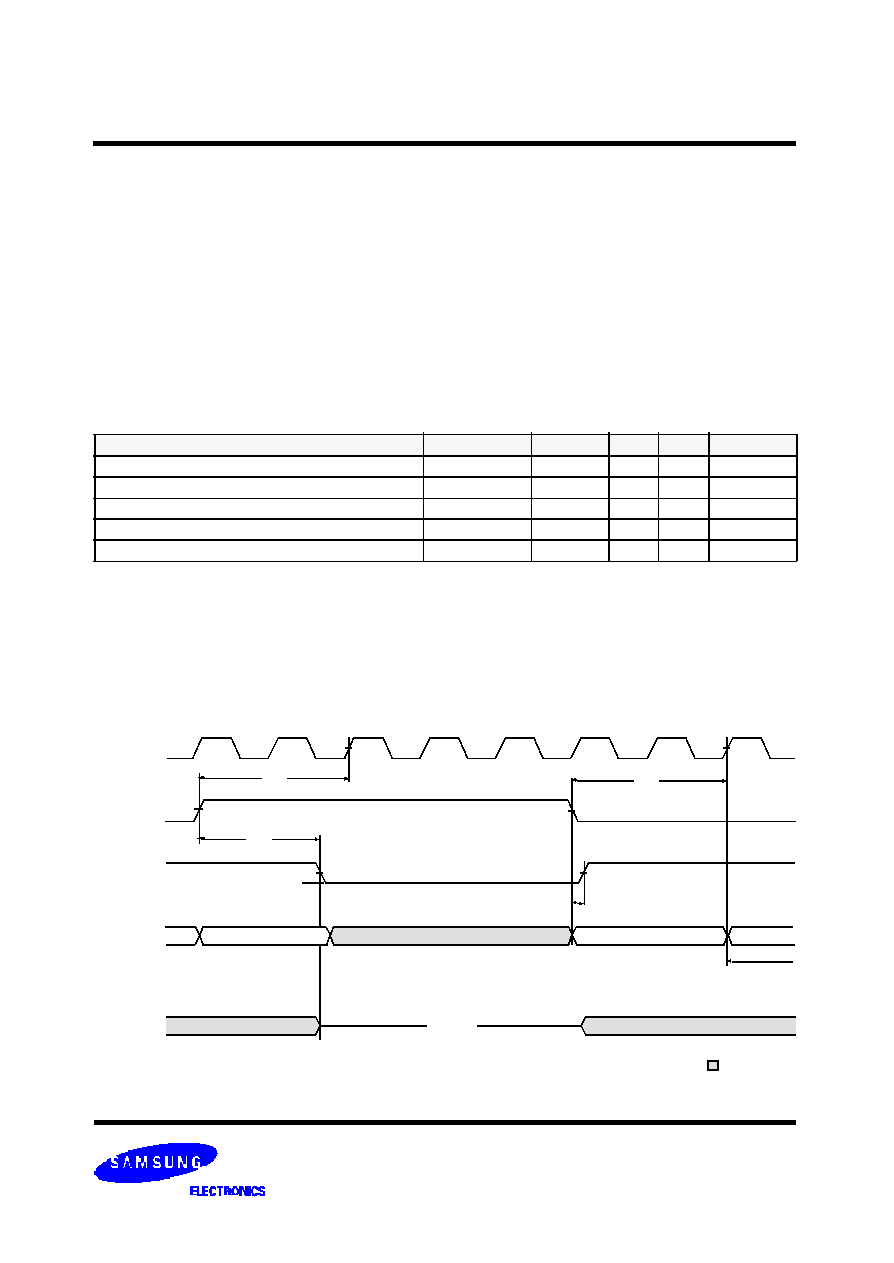
K7N163245A
512Kx36/32 & 1Mx18 Pipelined NtRAM
TM
- 22 -
Rev 2.1
April 2003
K7N161845A
K7N163645A
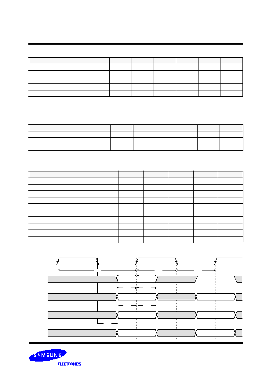
T
I
M
I
N
G
W
A
V
E
F
O
R
M
O
F
W
R
T
E
C
Y
C
L
E
C
l
o
c
k
A
d
d
r
e
s
s
W
R
I
T
E
C
S
A
D
V
D
a
t
a
I
n
t
C
H
t
C
L
A
2
A
3
D
2
-
1
D
1
-
1
D
2
-
2
D
2
-
3
D
2
-
4
D
3
-
1
D
3
-
2
D
3
-
3
O
E
D
a
t
a
O
u
t
t
D
S
t
D
H
D
o
n
t
C
a
r
e
U
n
d
e
f
i
n
e
d
t
C
Y
C
C
K
E
A
1
D
3
-
4
t
C
E
S
t
C
E
H
N
O
T
E
S
:
W
R
I
T
E
=
L
m
e
a
n
s
W
E
=
L
,
a
n
d
B
W
x
=
L
C
S
=
L
m
e
a
n
s
C
S
1
=
L
,
C
S
2
=
H
a
n
d
C
S
2
=
L
C
S
=
H
m
e
a
n
s
C
S
1
=
H
,
o
r
C
S
1
=
L
a
n
d
C
S
2
=
H
,
o
r
C
S
1
=
L
,
a
n
d
C
S
2
=
L
Q
0
-
4
t
H
Z
O
E
Q
0
-
3
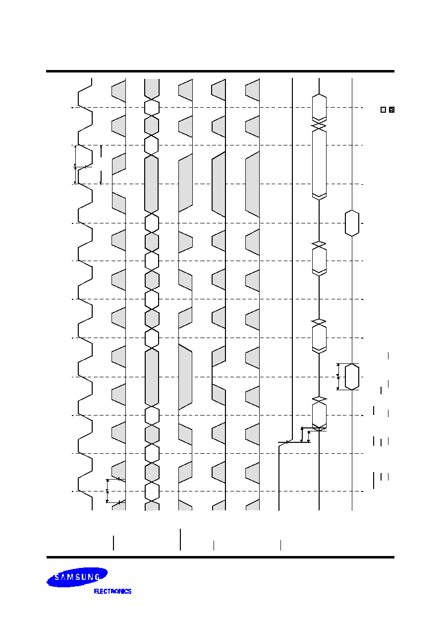
K7N163245A
512Kx36/32 & 1Mx18 Pipelined NtRAM
TM
- 23 -
Rev 2.1
April 2003
K7N161845A
K7N163645A
T
I
M
I
N
G
W
A
V
E
F
O
R
M
O
F
S
I
N
G
L
E
R
E
A
D
/
W
R
I
T
E
C
l
o
c
k
A
d
d
r
e
s
s
W
R
I
T
E
C
S
A
D
V
O
E
D
a
t
a
I
n
t
C
H
t
C
L
t
D
S
t
D
H
D
a
t
a
O
u
t
A
2
A
4
A
5
D
2
t
O
E
t
L
Z
O
E
Q
1
D
o
n
t
C
a
r
e
U
n
d
e
f
i
n
e
d
t
C
Y
C
C
K
E
t
C
E
S
t
C
E
H
A
1
A
3
A
7
A
6
Q
3
Q
4
Q
7
Q
6
D
5
N
O
T
E
S
:
W
R
I
T
E
=
L
m
e
a
n
s
W
E
=
L
,
a
n
d
B
W
x
=
L
C
S
=
L
m
e
a
n
s
C
S
1
=
L
,
C
S
2
=
H
a
n
d
C
S
2
=
L
C
S
=
H
m
e
a
n
s
C
S
1
=
H
,
o
r
C
S
1
=
L
a
n
d
C
S
2
=
H
,
o
r
C
S
1
=
L
,
a
n
d
C
S
2
=
L
A
9
A
8
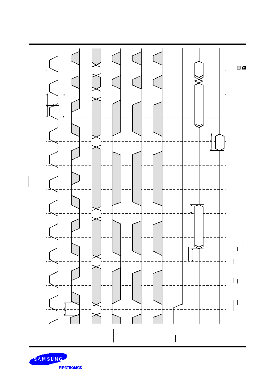
K7N163245A
512Kx36/32 & 1Mx18 Pipelined NtRAM
TM
- 24 -
Rev 2.1
April 2003
K7N161845A
K7N163645A
T
I
M
I
N
G
W
A
V
E
F
O
R
M
O
F
C
K
E
O
P
E
R
A
T
I
O
N
C
l
o
c
k
A
d
d
r
e
s
s
W
R
I
T
E
C
S
A
D
V
O
E
D
a
t
a
I
n
t
C
H
t
C
L
D
a
t
a
O
u
t
A
1
A
2
A
3
A
4
A
5
t
C
E
S
t
C
E
H
D
o
n
t
C
a
r
e
U
n
d
e
f
i
n
e
d
t
C
Y
C
C
K
E
t
D
S
t
D
H
D
2
Q
4
Q
1
N
O
T
E
S
:
W
R
I
T
E
=
L
m
e
a
n
s
W
E
=
L
,
a
n
d
B
W
x
=
L
C
S
=
L
m
e
a
n
s
C
S
1
=
L
,
C
S
2
=
H
a
n
d
C
S
2
=
L
C
S
=
H
m
e
a
n
s
C
S
1
=
H
,
o
r
C
S
1
=
L
a
n
d
C
S
2
=
H
,
o
r
C
S
1
=
L
,
a
n
d
C
S
2
=
L
t
C
D
t
L
Z
C
t
H
Z
C
Q
3
A
6
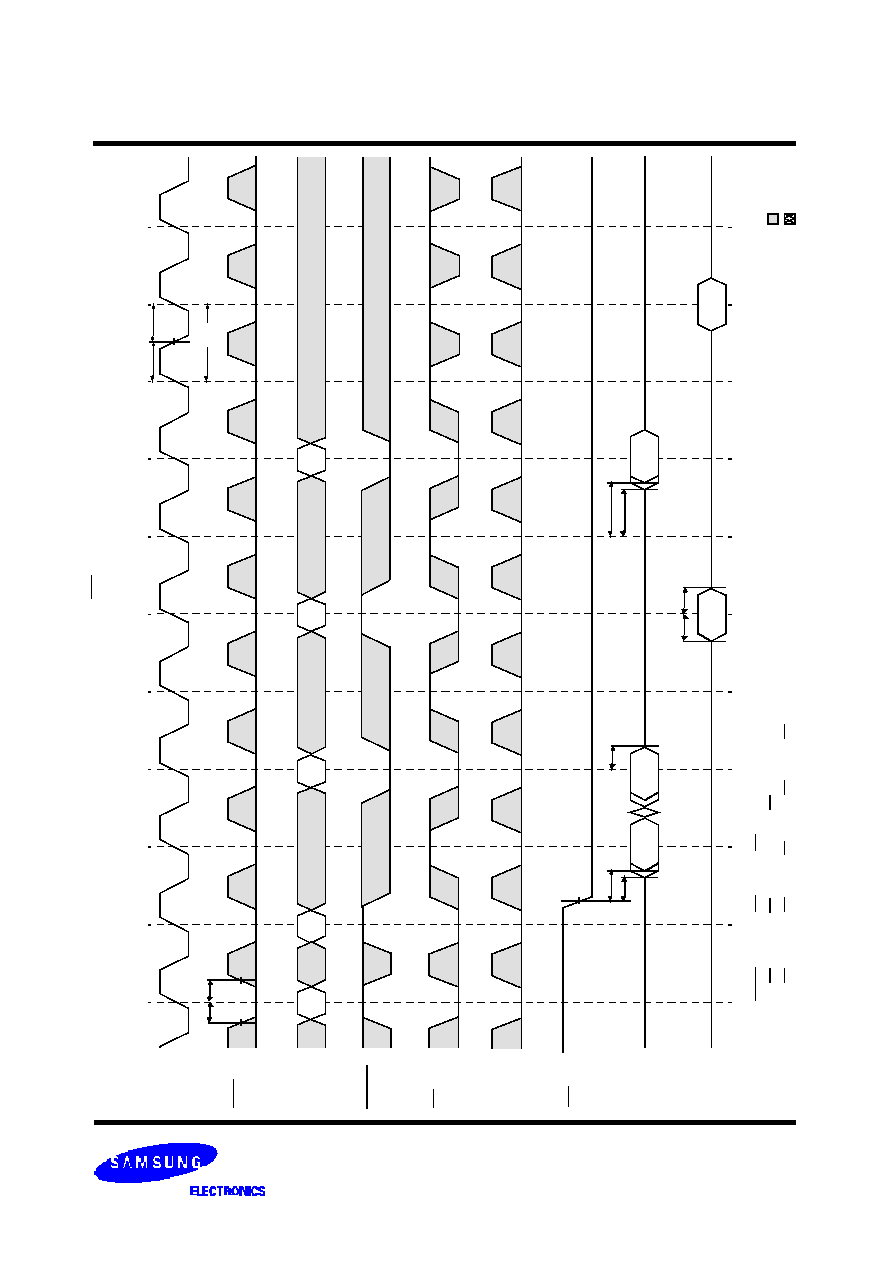
K7N163245A
512Kx36/32 & 1Mx18 Pipelined NtRAM
TM
- 25 -
Rev 2.1
April 2003
K7N161845A
K7N163645A
T
I
M
I
N
G
W
A
V
E
F
O
R
M
O
F
C
S
O
P
E
R
A
T
I
O
N
C
l
o
c
k
A
d
d
r
e
s
s
W
R
I
T
E
C
S
A
D
V
O
E
D
a
t
a
I
n
t
C
H
t
C
L
D
a
t
a
O
u
t
A
1
A
2
A
3
A
4
A
5
D
o
n
t
C
a
r
e
U
n
d
e
f
i
n
e
d
t
C
Y
C
C
K
E
D
5
Q
4
t
C
E
S
t
C
E
H
Q
1
Q
2
t
O
E
t
L
Z
O
E
D
3
t
C
D
t
L
Z
C
N
O
T
E
S
:
W
R
I
T
E
=
L
m
e
a
n
s
W
E
=
L
,
a
n
d
B
W
x
=
L
C
S
=
L
m
e
a
n
s
C
S
1
=
L
,
C
S
2
=
H
a
n
d
C
S
2
=
L
C
S
=
H
m
e
a
n
s
C
S
1
=
H
,
o
r
C
S
1
=
L
a
n
d
C
S
2
=
H
,
o
r
C
S
1
=
L
,
a
n
d
C
S
2
=
L
t
H
Z
C
t
D
H
t
D
S
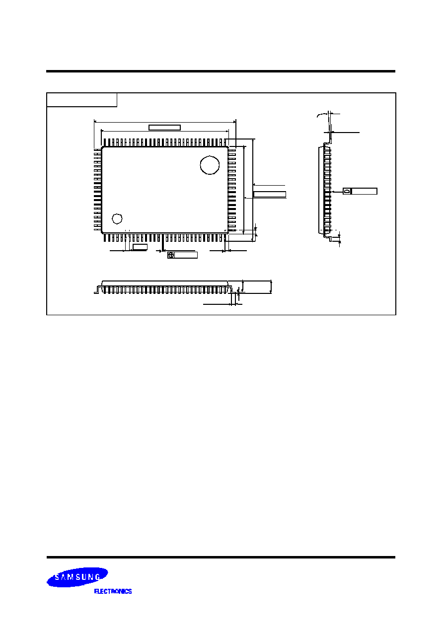
K7N163245A
512Kx36/32 & 1Mx18 Pipelined NtRAM
TM
- 26 -
Rev 2.1
April 2003
K7N161845A
K7N163645A
PACKAGE DIMENSIONS
0.10 MAX
0~8
∞
22.00
±
0.30
20.00
±
0.20
16.00
±
0.30
14.00
±
0.20
1.40
±
0.10
1.60 MAX
0.05 MIN
(0.58)
0.50
±
0.10
#1
(0.83)
0.50
±
0.10
100-TQFP-1420A
0.65
0.30
±
0.10
0.10 MAX
+ 0.10
- 0.05
0.127
Units ; millimeters/Inches
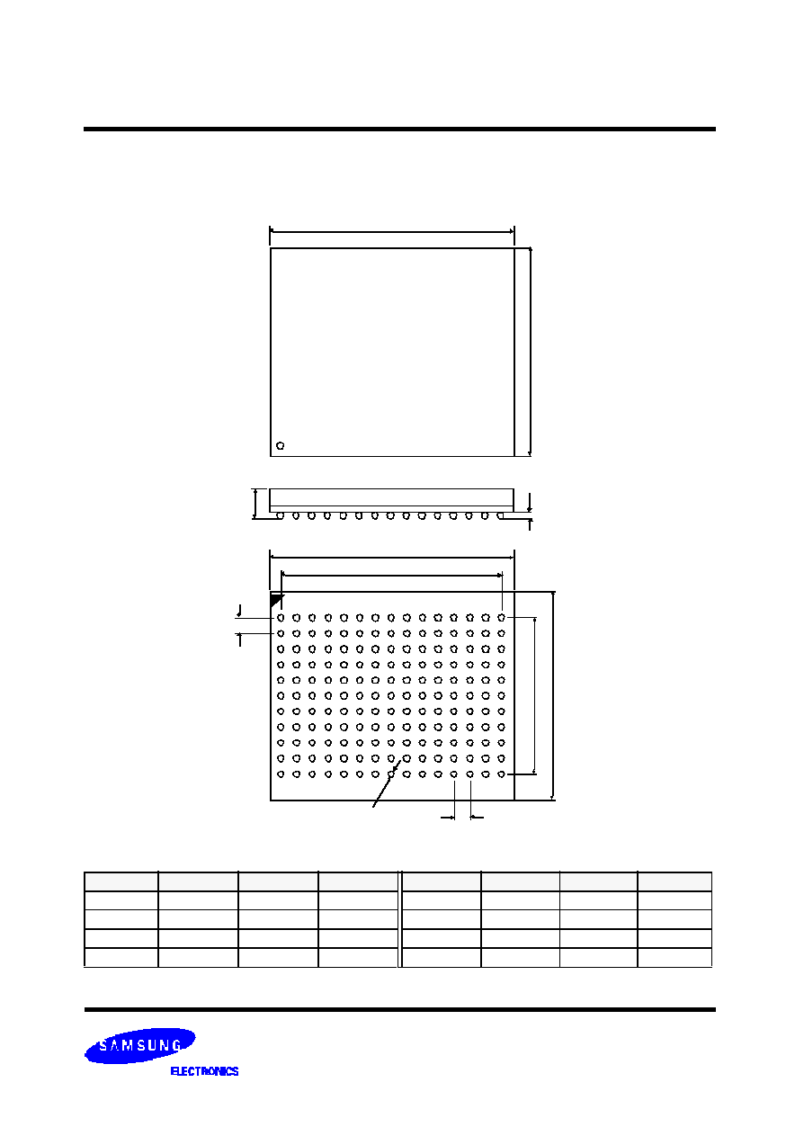
K7N163245A
512Kx36/32 & 1Mx18 Pipelined NtRAM
TM
- 27 -
Rev 2.1
April 2003
K7N161845A
K7N163645A
165 FBGA PACKAGE DIMENSIONS
C
Side View
13mm x 15mm Body, 1.0mm Bump Pitch, 11x15 Ball Array
F
A
H
G
B
Bottom View
Top View
A
B
D
E
E
Symbol
Value
Units
Note
Symbol
Value
Units
Note
A
15
±
0.1
mm
E
1.0
mm
B
13
±
0.1
mm
F
14.0
mm
C
1.3
±
0.1
mm
G
10.0
mm
D
0.35
±
0.05
mm
H
0.5
±
0.05
mm
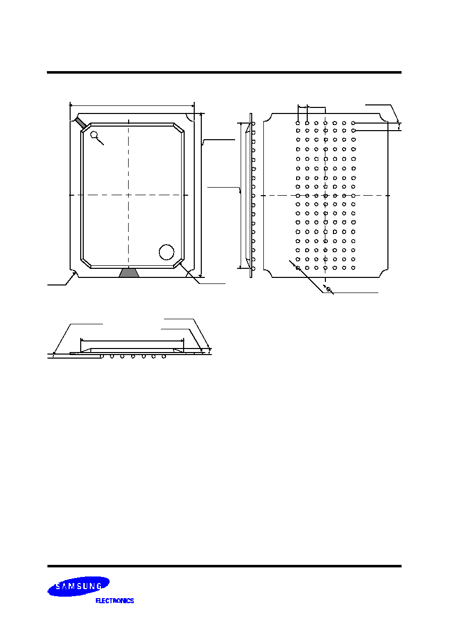
K7N163245A
512Kx36/32 & 1Mx18 Pipelined NtRAM
TM
- 28 -
Rev 2.1
April 2003
K7N161845A
K7N163645A
119BGA PACKAGE DIMENSIONS
0.750
±
0.15
1.27
1.27
12.50
±
0.10
0.60
±
0.10
0.60
±
0.10
1.50REF
C1.00
C0.70
14.00
±
0.10
22.00
±
0.10
20.50
±
0.10
NOTE
:
1. All Dimensions are in Millimeters.
2. Solder Ball to PCB Offset : 0.10 MAX.
3. PCB to Cavity Offset : 0.10 MAX.
Indicator of
Ball(1A) Location
NOTE :
119BGA is only supported with K7N161801A - HC13, K7N163645A - HC16, K7N161845A - HC13 and K7N163645 - HC16.