
K7P401823M
- 1 -
K7P403623M
128Kx36 & 256Kx18 SRAM
Rev 2.0
Oct. 2000
Document Title
128Kx36 & 256Kx18 Synchronous Pipelined SRAM
Revision History
Rev. No.
Rev. 0.0
Rev. 0.1
Rev. 0.2
Rev. 0.3
Rev. 1.0
Rev. 2.0
Remark
Preliminary
Preliminary
Preliminary
Preliminary
Final
History
- Preliminary specification release
- Change specification format.
No change was made in parameters.
- Updated Part Number and Pin Description.
Updated and added Input/Output Voltage Level and V
DDQ
Updated DC Characteristics and Pin Capacitance.
Updated AC Characteristics, Test Conditions and Timing Wave Form.
For JTAG, updated Vendor Definition and added t
SVCH
/t
CHSX.
- Updated PECL Clock Input Level, Output Leakage Current
Updated 119BGA Package Thermal Characteristics
- Final specification release
- Single ended LVCMOS clock operation added
Draft Date
April, 1997
Jan. 1998
Aug. 1998
Dec. 1998
Oct. 2000
The attached data sheets are prepared and approved by SAMSUNG Electronics. SAMSUNG Electronics CO., LTD. reserve the right to change the
specifications. SAMSUNG Electronics will evaluate and reply to your requests and questions on the parameters of this device. If you have any ques-
tions, please contact the SAMSUNG branch office near your office, call or cortact Headquarters.
K7P401823M
- 2 -
K7P403623M
128Kx36 & 256Kx18 SRAM
Rev 2.0
Oct. 2000
PIN DESCRIPTION
Pin Name
Pin Description
Pin Name
Pin Description
K, K
Differential Clocks(PECL Level)
V
DDQ
Output Power Supply
SAn
Synchronous Address Input
M
1
, M
2
Read Protocol Mode Pins ( M
1
=V
DD
, M
2
=V
SS
)
DQn
Bi-directional Data Bus
G
Asynchronous Output Enable
SW
Synchronous Global Write Enable
SS
Synchronous Select
SWa
Synchronous Byte a Write Enable
TCK
JTAG Test Clock
SWb
Synchronous Byte b Write Enable
TMS
JTAG Test Mode Select
SWc
Synchronous Byte c Write Enable
TDI
JTAG Test Data Input
SWd
Synchronous Byte d Write Enable
TDO
JTAG Test Data Output
ZZ
Asynchronous Power Down
V
SS
GND
V
DD
Core Power Supply
NC
No Connection
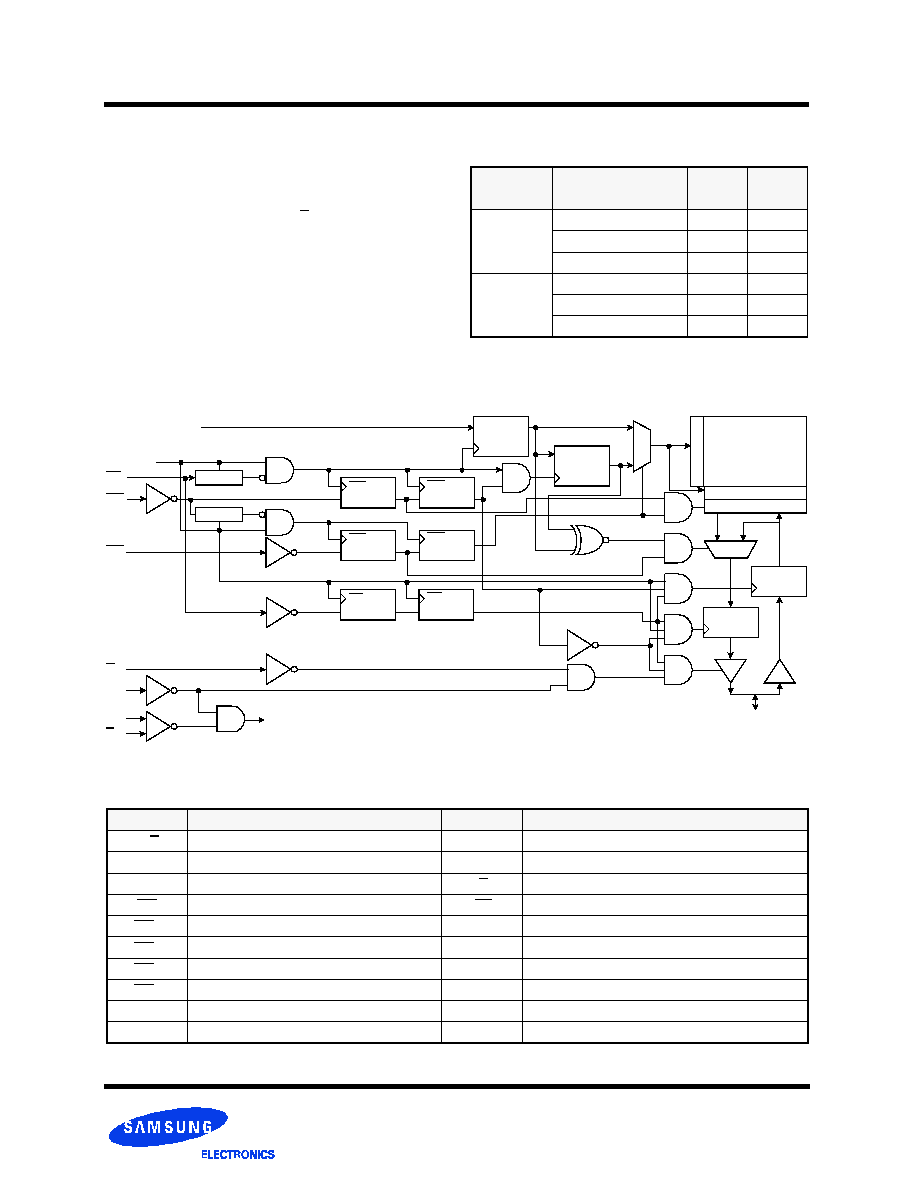
128Kx36 & 256Kx18 Synchronous Pipelined SRAM
FEATURES
FUNCTIONAL BLOCK DIAGRAM
∑ 128Kx36 or 256Kx18 Organizations.
∑ 3.3V Core/ Output Power Supply.
∑ LVTTL 3.3V Input and Output Levels.
∑ Differential, PECL Clock Inputs K, K.
or Single ended LVCMOS Clock
∑ Synchronous Read and Write Operation
∑ Registered Input and Latched Output
∑ Internal Pipeline Latches to Support Late Write.
∑ Byte Write Capability(four byte write selects, one for each 9 bits)
∑ Synchronous or Asynchronous Output Enable.
∑ Power Down Mode via ZZ Signal.
∑ JTAG 1149.1 Compatible Test Access port.
∑ 119(7x17) Pin Ball Grid Array Package(14mmx22mm).
Organiza-
tion
Part Number
Cycle
Time
Access
Time
128Kx36
K7P403623M-H65
6
6.5
K7P403623M-H70
6.5
7.0
K7P403623M-H75
7
7.5
256Kx18
K7P401823M-H65
6
6.5
K7P401823M-H70
6.5
7.0
K7P401823M-H75
7
7.5
SA[0:16] or SA[0:17]
CK
SS
SW
SWx
G
128Kx36
Data In
ZZ
DQx[1:9]
(x=a, b, c, d)
or (x=a, b)
(x=a, b, c, d)
or (x=a, b)
K
K
CK
or
256Kx18
Array
R
o
w
D
e
c
o
d
e
r
Column Decoder
Write/Read Circuit
Register
0 1
Data Out
Latch
1
Read
Address
Register
Write
Address
Register
Latch
SW
Register
SW
Register
Latch
SWx
Register
SWx
Register
SS
Register
SS
Register
0

K7P401823M
- 3 -
K7P403623M
128Kx36 & 256Kx18 SRAM
Rev 2.0
Oct. 2000
PACKAGE PIN CONFIGURATIONS
(TOP VIEW)
K7P403623M(128Kx36)
NOTE : 1. NC* is used for the Boundary Scan.
2. NC** is reserved for TRST input
.
3. NC*** is reserved for HSTL interface.
1
2
3
4
5
6
7
A
V
DDQ
SA
13
SA
10
NC
SA
7
SA
4
V
DDQ
B
NC
NC
SA
9
NC
SA
8
NC
NC
C
NC
SA
12
SA
11
V
DD
SA
6
SA
5
NC
D
DQc
8
DQc
9
V
SS
NC*
V
SS
DQb
9
DQb
8
E
DQc
6
DQc
7
V
SS
SS
V
SS
DQb
7
DQb
6
F
V
DDQ
DQc
5
V
SS
G
V
SS
DQb
5
V
DDQ
G
DQc
3
DQc
4
SWc
NC*
SWb
DQb
4
DQb
3
H
DQc
1
DQc
2
V
SS
NC*
V
SS
DQb
2
DQb
1
J
V
DDQ
V
DD
NC***
V
DD
NC***
V
DD
V
DDQ
K
DQd
1
DQd
2
V
SS
K
V
SS
DQa
2
DQa
1
L
DQd
3
DQd
4
SWd
K
SWa
DQa
4
DQa
3
M
V
DDQ
DQd
5
V
SS
SW
V
SS
DQa
5
V
DDQ
N
DQd
6
DQd
7
V
SS
SA
16
V
SS
DQa
7
DQa
6
P
DQd
8
DQd
9
V
SS
SA
0
V
SS
DQa
9
DQa
8
R
NC
SA
15
M
1
V
DD
M
2
SA
2
NC
T
NC
NC
SA
14
SA
1
SA
3
NC
ZZ
U
V
DDQ
TMS
TDI
TCK
TDO
NC**
V
DDQ
KM718FV4022(256Kx18)
NOTE : 1. NC* is used for the Boundary Scan.
2. NC** is reserved for TRST input
.
3. NC*** is reserved for HSTL interface.
1
2
3
4
5
6
7
A
V
DDQ
SA
13
SA
10
NC
SA
7
SA
4
V
DDQ
B
NC
NC
SA
9
NC
SA
8
NC
NC
C
NC
SA
12
SA
11
V
DD
SA
6
SA
5
NC
D
DQb
1
NC
V
SS
NC*
V
SS
DQa
9
NC
E
NC
DQb
2
V
SS
SS
V
SS
NC
DQa
8
F
V
DDQ
NC
V
SS
G
V
SS
DQa
7
V
DDQ
G
NC
DQb
3
SWb
NC*
NC
NC
DQa
6
H
DQb
4
NC
V
SS
NC*
V
SS
DQa
5
NC
J
V
DDQ
V
DD
NC***
V
DD
NC***
V
DD
V
DDQ
K
NC
DQb
5
V
SS
K
V
SS
NC
DQa
4
L
DQb
6
NC
NC
K
SWa
DQa
3
NC
M
V
DDQ
DQb
7
V
SS
SW
V
SS
NC
V
DDQ
N
DQb
8
NC
V
SS
SA
16
V
SS
DQa
2
NC
P
NC
DQb
9
V
SS
SA
1
V
SS
NC
DQa
1
R
NC
SA
15
M
1
V
DD
M
2
SA
2
NC
T
NC
SA
17
SA
14
NC
SA
3
SA
0
ZZ
U
V
DDQ
TMS
TDI
TCK
TDO
NC**
V
DDQ

K7P401823M
- 4 -
K7P403623M
128Kx36 & 256Kx18 SRAM
Rev 2.0
Oct. 2000
FUNCTION DESCRIPTION
The K7P403623M andK7P401823M are 4,718,592 bit Synchronous SRAM. It is organized as 131,072 words of 36 bits(or 262,144
words of 18 bits) and is implemented in SAMSUNG's advanced CMOS technology.
Single differential PECL level K clocks or single ended LVCMOS clock are used to initiate the read/write operation and all internal
operations are self-timed. At the rising edge of K clock, all addresses, Write Enables, Synchronous Select and Data Ins are regis-
tered internally. Data outputs are updated from output latches of the falling edge of K clock. An internal write data buffer allows write
data to follow one cycle after addresses and controls. The package is 119(7x17) Ball Grid Array with balls on a 1.27mm pitch.
Read Operation
During reads, the address is registered during the clock rising edge and the internal array is read. The data is driven to the CPU in
the following cycle. SS is driven low during this cycle, signaling that the SRAM should drive out the data.
During consecutive read cycles where the address is the same, the data output must be held constantly without any glitches. This
characteristic is because the SRAM will be read by devices that will operate slower than the SRAM frequency and will require multi-
ple SRAM cycles to perform a single read operation.
Write(Store) Operation
All addresses and SW are both sampled on the clock rising edge. SW is low on the rising clock. Write data is sampled on the rising
clock, one cycle after write address and SW have been sampled by the SRAM. SS will be driven low during the same cycle that the
Address, SW and SW[a:d] are valid to signal that a valid operations is on the Address and Control Input.
Pipelined write are supported. This is done by using write data buffers on the SRAM that capture the write addresses on one write
cycle, and write the array on the next write cycle. The "next write cycle" can actually be many cycles away, broken by a series of
read cycles. Byte writes are supported. The byte write signals SW[a:d] signal which 9-bit bytes will be writen. Timing of SW[a:d] is the
same as the SW signal.
Bypass Read Operation
Since write data is not fully written into the array on first write cycle, there is a need to sense the address in case a future read is to
be done from the location that has not been written yet. For this case, the address comparator check to see if the new read address
is the same as the contents of the stored write address Latch. If the contents match, the read data must be supplied from the stored
write data latch with standard read timing. If there is no match, the read data comes from the SRAM array. The bypassing of the
SRAM array occurs on a byte by byte basis. If one byte is written and the other bytes are not, read data from the last written will have
new byte data from the write data buffer and the other bytes from the SRAM array.
Low Power Dissipation Mode
During normal operation, asynchronous signal ZZ must be pulled low. Low Power Mode is enabled by switching ZZ high. When the
SRAM is in Power Down Mode, the outputs will go to a Hi-Z state and the SRAM will draw standby current. SRAM data will be pre-
served and a recovery time(t
ZZR
) is required before the SRAM resumes to normal operation.
TRUTH TABLE
K
ZZ
G
SS
SW
SWa
SWb
SWc
SWd
DQa
DQb
DQc
DQd
Operation
X
H
X
X
X
X
X
X
X
Hi-Z
Hi-Z
Hi-Z
Hi-Z Power Down Mode. No Operation
X
L
H
X
X
X
X
X
X
Hi-Z
Hi-Z
Hi-Z
Hi-Z Output Disabled. No Operation
L
L
H
X
X
X
X
X
Hi-Z
Hi-Z
Hi-Z
Hi-Z Output Disabled. No Operation
L
L
L
H
X
X
X
X
D
OUT
D
OUT
D
OUT
D
OUT
Read Cycle
L
X
L
L
H
H
H
H
Hi-Z
Hi-Z
Hi-Z
Hi-Z No Bytes Written
L
X
L
L
L
H
H
H
D
IN
Hi-Z
Hi-Z
Hi-Z Write first byte
L
X
L
L
H
L
H
H
Hi-Z
D
IN
Hi-Z
Hi-Z Write second byte
L
X
L
L
H
H
L
H
Hi-Z
Hi-Z
D
IN
Hi-Z Write third byte
L
X
L
L
H
H
H
L
Hi-Z
Hi-Z
Hi-Z
D
IN
Write fourth byte
L
X
L
L
L
L
L
L
D
IN
D
IN
D
IN
D
IN
Write all byte

K7P401823M
- 5 -
K7P403623M
128Kx36 & 256Kx18 SRAM
Rev 2.0
Oct. 2000
ABSOLUTE MAXIMUM RATINGS
NOTE : Stresses greater than those listed under "Absolute Maximum Ratings" may cause permanent damage to the device. This is a stress rating only
and functional operation of the device at these or any other conditions above those indicated in the operating sections of this specification is not
implied. Exposure to absolute maximum rating conditions for extended periods may affect reliability.
Parameter
Symbol
Value
Unit
Core Supply Voltage Relative to V
SS
V
DD
-0.5 to 3.9
V
Output Supply Voltage Relative to V
SS
V
DDQ
V
DD
V
Voltage on any I/O pin Relative to V
SS
V
TERM
-0.5 to V
DD
+0.5
V
Maximum Power Dissipation
P
D
3
W
Output Short-Circuit Current
I
OUT
25
mA
Operating Temperature
T
OPR
0 to 70
∞
C
Storage Temperature
T
STG
-55 to 125
∞
C
DC CHARACTERISTICS
NOTE :1. Minimum cycle. I
OUT
=0mA.
2. 50% read cycles.
Parameter
Symbol
Min
Max
Unit
Note
Average Power Supply Operating Current-x36
(V
IN
=V
IH
or V
IL
, ZZ & SS=V
IL
)
I
DD65
I
DD7
I
DD75
-
600
550
500
mA
1, 2
Average Power Supply Operating Current-x18
(V
IN
=V
IH
or V
IL
, ZZ & SS=V
IL
)
I
DD65
I
DD7
I
DD75
-
550
500
450
mA
1, 2
Power Supply Standby Current
(V
IN
=V
IH
or V
IL
, ZZ=V
IH
)
I
SB
-
60
mA
1
Input Leakage Current
(V
IN
=V
SS
or V
DDQ
)
I
LI
-1
1
µ
A
Output Leakage Current
(V
OUT
=V
SS
or V
DDQ
, ZZ=V
IH
, G=V
IH
)
I
LO
-1
1
µ
A
Output High Voltage(I
OH
=-4mA) for V
DDQ
=3.3V
Output High Voltage(I
OH
=-4mA) for V
DDQ
=2.5V
V
OH1
V
OH2
2.4
2.0
V
DDQ
V
Output Low Voltage(I
OL
=4mA)
V
OL
V
SS
0.4
V
RECOMMENDED DC OPERATING CONDITIONS
NOTE
1. For operation with differential PECL clock inputs.
2. For operation with single ended LVCMOS clock input.
Parameter
Symbol
Min
Typ
Max
Unit
Note
Core Power Supply Voltage
V
DD
3.15
3.3
3.45
V
Output Power Supply Voltage
V
DDQ
2.35
2.5
3.45
V
Input High Level
V
IH
1.7
-
V
DD
+0.3
V
Input Low Level
V
IL
-0.3
-
0.7
V
PECL Clock Input High Level
V
IH
-PECL
2.135
-
2.420
V
1
PECL Clock Input Low Level
V
IL
-PECL
1.490
-
1.825
V
1
Clock Input Signal Voltage
V
IN
-0.3
-
3.45
V
2
Clock Input Differential Voltage
V
DIF
-CLK
0.2
-
V
DD
+0.6
V
2
Clock Input Common Mode Voltage
V
CM
-CLK
1.1
-
2.1
V
2
Operating Junction Temperature
T
J
10
-
110
∞
C

K7P401823M
- 6 -
K7P403623M
128Kx36 & 256Kx18 SRAM
Rev 2.0
Oct. 2000
AC CHARACTERISTICS
Parameter
Symbol
-65
-70
-75
Unit
Note
Min
Max
Min
Max
Min
Max
Clock Cycle Time
t
KHKH
6.0
-
6.5
-
7.0
-
ns
Clock High Pulse Width
t
KHKL
2.0
-
2.0
-
2.0
-
ns
Clock Low Pulse Width
t
KLKH
2.0
-
2.0
-
2.0
-
ns
Clock High to Output Valid
t
KHQV
-
6.5
-
7.0
-
7.5
ns
Clock Low to Output Valid
t
KLQV
-
2.5
-
2.5
-
3.0
ns
Clock Low to Output Hold
t
KLQX
0.5
-
0.5
-
0.5
-
ns
Address Setup Time
t
AVKH
0.5
-
0.5
-
0.5
-
ns
Address Hold Time
t
KHAX
1.0
-
1.0
-
1.0
-
ns
Write Data Setup Time
t
DVKH
0.5
-
0.5
-
0.5
-
ns
Write Data Hold Time
t
KHDX
1.0
-
1.0
-
1.0
-
ns
SW, SW[a:d] Setup Time
t
WVKH
0.5
-
0.5
-
0.5
-
ns
SW, SW[a:d] Hold Time
t
KHWX
1.0
-
1.0
-
1.0
-
ns
SS Setup Time
t
SVKH
0.5
-
0.5
-
0.5
-
ns
SS Hold Time
t
KHSX
1.0
-
1.0
-
1.0
-
ns
Clock High to Output Hi-Z
t
KHQZ
-
2.5
-
3.0
-
3.5
ns
Clock Low to Output Low-Z
t
KLQX1
0.5
-
0.5
-
0.5
-
ns
G High to Output High-Z
t
GHQZ
-
2.5
-
3.0
-
3.5
ns
G Low to Output Low-Z
t
GLQX
0.5
-
0.5
-
0.5
-
ns
G Low to Output Valid
t
GLQV
-
2.5
-
3.0
-
3.5
ns
ZZ High to Power Down(Sleep Time)
t
ZZE
-
6.5
-
7.0
-
7.5
ns
ZZ Low to Recovery(Wake-up Time)
t
ZZR
-
6.0
-
6.5
-
7.0
ns
Z0=50
50
1.25V
*Capacitive load consists of all components
AC TEST OUTPUT LOAD
Dout
of the tester environment
20pF*
PIN CAPACITANCE
NOTE : Periodically sampled and not 100% tested.(dV=0V, f=1MHz)
Parameter
Symbol
Typ
Max
Unit
Input Capacitance
C
IN
4
5
pF
Output Capacitance
C
OUT
7
8
pF
AC TEST CONDITIONS
Parameter
Symbol
Value
Unit
Core Power Supply Voltage
V
DD
3.15~3.45
V
Output Power Supply Voltage
V
DDQ
2.4~2.6
V
Input High/Low Level
V
IH
/V
IL
1.7/0.7
V
Clock Input High/Low Level(PECL) V
IH/
V
IL
2.4/1.5
V
Input Rise/Fall Time
T
R
/T
F
1.0/1.0
ns
Clock Input Rise/Fall Time(PECL)
T
R
/T
F
1.0/1.0
ns
Input and Out Timing Reference Level
1.25
V
Clock Input Timing Reference Level
Cross Point
V
K7P401823M
- 7 -
K7P403623M
128Kx36 & 256Kx18 SRAM
Rev 2.0
Oct. 2000
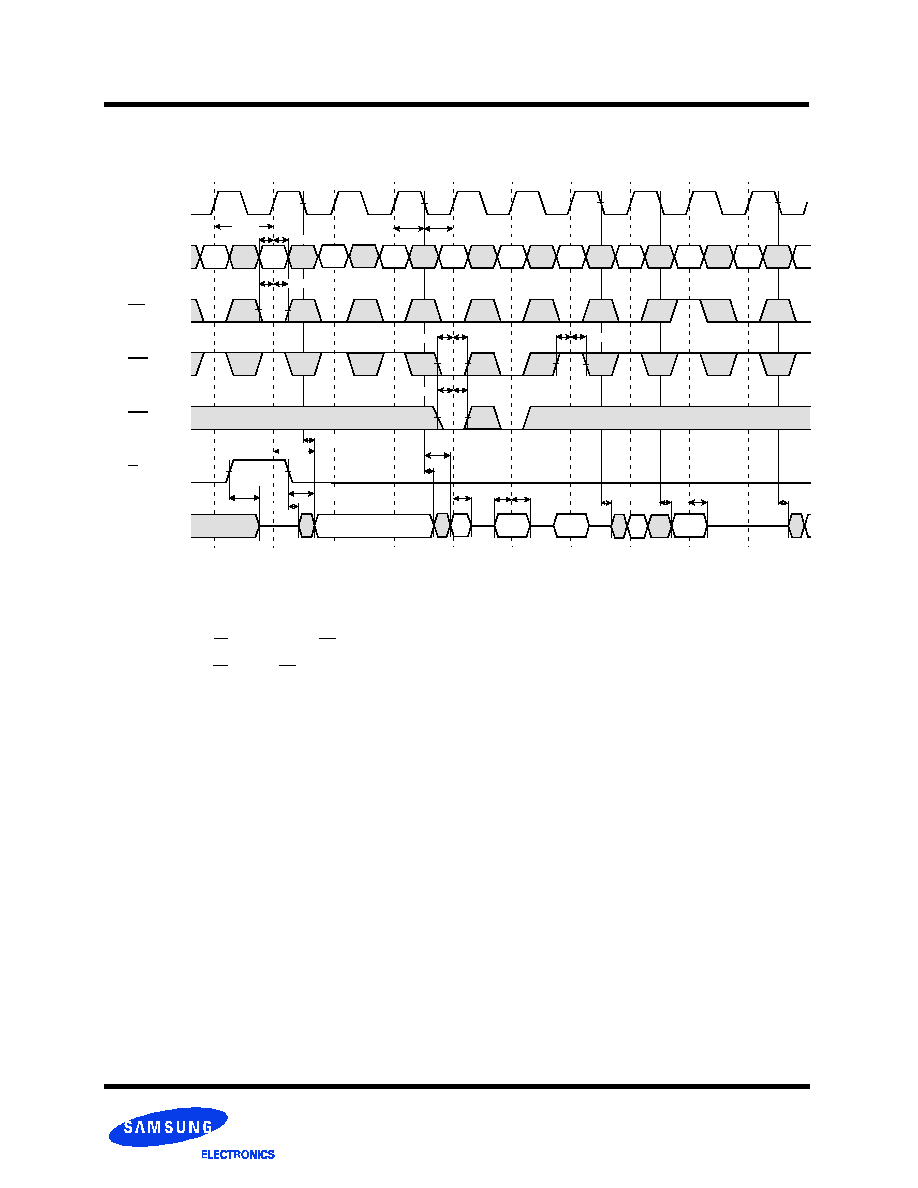
TIMING WAVEFORMS OF NORMAL ACTIVE CYCLES
NOTE
1. D3 is the input data written in memory location A3.
2. Q4 is the output data read from the write data buffer(not from the cell array), as a result of address A4 being a match from the last write
cycle address.
3. Data is valid at the output at the later of t
KHQV
following the rising clock edge, or t
KLQV
following the fallowing clock edge.
4. When SS is sampled high or SW is sampled low on the rising edge of clock, the outputs go into Hi-Z state no later than t
KHQZ
following
the rising clock edge.
5. When SS is low and SW is high on the rising edge of clock, the outputs go into Low-Z state(being driven) no earlier than t
KLQX1
following
the next falling edge of clock.
6. When the SRAM is deselected, the output goes Hi-Z at t
KHQZ
following the rising clock edge. On the next read cycle, note that the
SRAM output do not leave the Hi-Z state until t
KLQX1
after the falling clock edge.
1
2
3
4
5
6
7
8
K
SAn
SS
SW
SWx
DQn
G
A
1
A
2
A
3
A
4
A
5
A
4
A
6
A
7
Q
1
Q
2
D
3
D
4
Q
5
Q
4
t
KHKH
t
KHAX
t
AVKH
t
KHKL
t
KLKH
t
KHSX
t
SVKH
t
WVKH
t
KHWX
t
WVKH
t
KHWX
t
KLQV
t
KHQZ
t
WVKH
t
KHWX
t
KHQV
t
KHQZ
t
DVKH
t
KHDX
t
GHQZ
t
GLQV
t
KLQV
A
1
t
KLQX
t
KLQV
t
GLQX
t
KLQX1
t
KLQX1
9

K7P401823M
- 8 -
K7P403623M
128Kx36 & 256Kx18 SRAM
Rev 2.0
Oct. 2000
TIMING WAVEFORMS OF STANDBY CYCLES
1
2
3
4
5
6
7
8
K
SAn
SS
SW
SWx
DQn
ZZ
A
2
A
1
A
2
A
3
Q
2
Q
3
Q
2
A
1
A
3
Q
1
Q
1
t
KHKH
t
ZZE
t
ZZR
t
KHQV
t
KHQV

K7P401823M
- 9 -
K7P403623M
128Kx36 & 256Kx18 SRAM
Rev 2.0
Oct. 2000
JTAG Instruction Coding
NOTE
1. Places DQs in Hi-Z in order to sample all input data regardless of
other SRAM inputs.
2. TDI is sampled as an input to the first ID register to allow for the serial
shift of the external TDI data.
3. Bypass register is initiated to VSS when BYPASS instruction is
invoked. The Bypass Register also holds serially loaded TDI when
exiting the Shift DR states.
4. SAMPLE instruction dose not places DQs in Hi-Z.
IR2 IR1 IR0 Instruction
TDO Output
Notes
0
0
0 SAMPLE-Z Boundary Scan Register
1
0
0
1 IDCODE
Identification Register
2
0
1
0 SAMPLE-Z Boundary Scan Register
1
0
1
1 BYPASS
Bypass Register
3
1
0
0 SAMPLE
Boundary Scan Register
4
1
0
1 BYPASS
Bypass Register
3
1
1
0 BYPASS
Bypass Register
3
1
1
1 BYPASS
Bypass Register
3
IEEE 1149.1 TEST ACCESS PORT AND BOUNDARY SCAN-JTAG
This part contains an IEEE standard 1149.1 Compatible Teat Access Port(TAP). The package pads are monitored by the Serial
Scan circuitry when in test mode. This is to support connectivity testing during manufacturing and system diagnostics. Internal data is
not driven out of the SRAM under JTAG control. In conformance with IEEE 1149.1, the SRAM contains a TAP controller, Instruction
Register, Bypass Register and ID register. The TAP controller has a standard 16-state machine that resets internally upon power-up,
therefore, TRST signal is not required. It is possible to use this device without utilizing the TAP. To disable the TAP controller without
interfacing with normal operation of the SRAM, TCK must be tied to V
SS
to preclude mid level input. TMS and TDI are designed so an
undriven input will produce a response identical to the application of a logic 1, and may be left unconnected. But they may also be
tied to V
DD
through a resistor. TDO should be left unconnected.
JTAG Block Diagram
SRAM
CORE
BYPASS Reg.
Identification Reg.
Instruction Reg.
Control Signals
TAP Controller
TDO
M
2
M
1
TDI
TMS
TCK
TAP Controller State Diagram
Test Logic Reset
Run Test Idle
0
1
1
1
1
0
0
0
1
0
1
1
0
0
0
1
0
1
1
1
0
0
0
0
0
0
0
Select DR
Capture DR
Shift DR
Exit1 DR
Pause DR
Exit2 DR
Update DR
Select IR
Capture IR
Shift IR
Exit1 IR
Pause IR
Exit2 IR
Update IR
1
1
1
1
1

K7P401823M
- 10
K7P403623M
128Kx36 & 256Kx18 SRAM
Rev 2.0
Oct. 2000
BOUNDARY SCAN EXIT ORDER(x36)
36
3B
SA
9
SA
8
5B
35
37
2B
NC
NC
6B
34
38
3A
SA
10
SA
7
5A
33
39
3C
SA
11
SA
6
5C
32
40
2C
SA
12
SA
5
6C
31
41
2A
SA
13
SA
4
6A
30
42
2D
DQc
9
DQb
9
6D
29
43
1D
DQc
8
DQb
8
7D
28
44
2E
DQc7
DQb
7
6E
27
45
1E
DQc
6
DQb
6
7E
26
46
2F
DQc
5
DQb
5
6F
25
47
2G
DQc
4
DQb
4
6G
24
48
1G
DQc
3
DQb
3
7G
23
49
2H
DQc
2
DQb
2
6H
22
50
1H
DQc
1
DQb
1
7H
21
51
3G
SWc
SWb
5G
20
52
4D
NC
G
4F
19
53
4E
SS
K
4K
18
54
4G
NC
K
4L
17
55
4H
NC
SWa
5L
16
56
4M
SW
DQa
1
7K
15
57
3L
SWd
DQa
2
6K
14
58
1K
DQd
1
DQa
3
7L
13
59
2K
DQd
2
DQa
4
6L
12
60
1L
DQd
3
DQa
5
6M
11
61
2L
DQd
4
DQa
6
7N
10
62
2M
DQd
5
DQa
7
6N
9
63
1N
DQd
6
DQa
8
7P
8
64
2N
DQd
7
DQa
9
6P
7
65
1P
DQd
8
ZZ
7T
6
66
2P
DQd
9
SA
3
5T
5
67
3T
SA
14
SA
2
6R
4
68
2R
SA
15
SA
1
4T
3
69
4N
SA
16
SA
0
4P
2
70
3R
M
1
M
2
5R
1
BOUNDARY SCAN EXIT ORDER(x18)
26
3B
SA
9
SA
8
5B
25
27
2B
NC
NC
6B
24
28
3A
SA
10
SA
7
5A
23
29
3C
SA
11
SA
6
5C
22
30
2C
SA
12
SA
5
6C
21
31
2A
SA
13
SA
4
6A
20
DQa
9
6D
19
32
1D
DQb
1
33
2E
DQb
2
DQa
8
7E
18
DQa
7
6F
17
34
2G
DQb
3
DQa
6
7G
16
DQa
5
6H
15
35
1H
DQb
4
36
3G
SWb
37
4D
NC
G
4F
14
38
4E
SS
K
4K
13
39
4G
NC
K
4L
12
40
4H
NC
SWa
5L
11
41
4M
SW
DQa
4
7K
10
42
2K
DQb
5
DQa
3
6L
9
43
1L
DQb
6
44
2M
DQb
7
DQa
2
6N
8
45
1N
DQb
8
DQa
1
7P
7
ZZ
7T
6
46
2P
DQb
9
SA
3
5T
5
47
3T
SA
14
SA
2
6R
4
48
2R
SA
15
49
4N
SA
16
SA
1
4P
3
50
2T
SA
17
SA
0
6T
2
51
3R
M
1
M
2
5R
1
SCAN REGISTER DEFINITION
Part
Instruction Register
Bypass Register
ID Register
Boundary Scan
128Kx36
3 bits
1 bits
32 bits
70 bits
256Kx18
3 bits
1 bits
32 bits
51 bits
ID REGISTER DEFINITION
Part
Revision Number
(31:28)
Part Configuration
(27:18)
Vendor Definition
(17:12)
Samsung JEDEC Code
(11: 1)
Start Bit(0)
128Kx36
0000
00101 00100
xxxxxx
00001001110
1
256Kx18
0000
00110 00011
xxxxxx
00001001110
1
NOTE : 1. Pins 6B and 2B are no connection pin to internal chip. These pins are place holders for 16M part and the scanned data are fixed to "0" for this
4M parts.

K7P401823M
- 11
K7P403623M
128Kx36 & 256Kx18 SRAM
Rev 2.0
Oct. 2000
JTAG DC OPERATING CONDITIONS
NOTE : 1. The input level of SRAM pin is to follow the SRAM DC specification.
Parameter
Symbol
Min
Typ
Max
Unit
Note
Power Supply Voltage
V
DD
3.15
3.3
3.45
V
Input High Level
V
IH
2.0
-
V
DD
+0.3
V
Input Low Level
V
IL
-0.3
-
0.8
V
Output High Voltage(I
OH
=-2mA)
V
OH
2.4
-
V
DD
V
Output Low Voltage(I
OL
=2mA)
V
OL
V
SS
-
0.4
V
JTAG TIMING DIAGRAM
JTAG AC TEST CONDITIONS
NOTE : 1. See SRAM AC test output load.
Parameter
Symbol
Min
Unit
Note
Input High/Low Level
V
IH
/V
IL
3.0/0.0
V
Input Rise/Fall Time
TR/TF
2.0/2.0
ns
Input and Output Timing Reference Level
1.5
V
1
TCK
TMS
TDI
TDO
t
CHCH
t
CHCL
t
CLCH
t
DVCH
t
CHDX
t
CLQV
t
MVCH
t
CHMX
JTAG AC Characteristics
Parameter
Symbol
Min
Max
Unit
Note
TCK Cycle Time
t
CHCH
50
-
ns
TCK High Pulse Width
t
CHCL
20
-
ns
TCK Low Pulse Width
t
CLCH
20
-
ns
TMS Input Setup Time
t
MVCH
5
-
ns
TMS Input Hold Time
t
CHMX
5
-
ns
TDI Input Setup Time
t
DVCH
5
-
ns
TDI Input Hold Time
t
CHDX
5
-
ns
SRAM Input Setup Time
t
SVCH
5
-
ns
SRAM Input Hold Time
t
CHSX
5
-
ns
Clock Low to Output Valid
t
CLQV
0
10
ns

K7P401823M
- 12
K7P403623M
128Kx36 & 256Kx18 SRAM
Rev 2.0
Oct. 2000
119 BGA PACKAGE DIMENSIONS
119 BGA PACKAGE THERMAL CHARACTERISTICS
Parameter
Symbol
Min
Typ
Max
Unit
Note
Junction to Ambient(at air flow of 1m/sec)
Theta_JA
-
-
17
∞
C/W
Junction to Case
Theta_JC
-
-
4
∞
C/W
Junction to Solder Ball
Theta_JB
-
-
10
∞
C/W
0.750
±
0.15
1.27
1.27
12.50
±
0.10
0.60
±
0.10
0.60
±
0.10
1.50REF
C1.00
C0.70
14.00
±
0.10
22.00
±
0.10
20.50
±
0.10
NOTE :
1. All Dimensions are in Millimeters.
2. Solder Ball to PCB Offset : 0.10 MAX.
3. PCB to Cavity Offset : 0.10 MAX.
Indicator of
Ball(1A) Location