Äîêóìåíòàöèÿ è îïèñàíèÿ www.docs.chipfind.ru
- 1 -
Rev 3.1
July. 2004
512Kx36 & 1Mx18 QDR
TM
II b4 SRAM
K7R163684B
K7R161884B
Document Title
512Kx36-bit,1Mx18-bit QDR
TM
II b4 SRAM
The attached data sheets are prepared and approved by SAMSUNG Electronics. SAMSUNG Electronics CO., LTD. reserve the right to change the
specifications. SAMSUNG Electronics will evaluate and reply to your requests and questions on the parameters of this device. If you have any ques-
tions, please contact the SAMSUNG branch office near your office, call or contact Headquarters.
Revision History
Rev. No.
0.0
0.1
0.2
0.3
0.4
0.5
0.6
0.7
1.0
2.0
3.0
3.1
Remark
Advance
Preliminary
Preliminary
Preliminary
Preliminary
Preliminary
Preliminary
Preliminary
Final
Final
Final
Final
History
1. Initial document.
1. Change the Boundary scan exit order.
2. Correct the Overshoot and Undershoot timing diagram.
1. Change JTAG Block diagram
1. Add the speed bin (-25)
1. Correct the JTAG ID register definition
2. Correct the AC timing parameter (delete the tKHKH Max value)
1. Change the Maximum Clock cycle time.
2. Correct the 165FBGA package ball size.
1. Add the power up/down sequencing comment.
2. Update the DC current parameter (Icc and Isb).
3. Change the Max. speed bin from -33 to -30.
1. Change the ISB1.
1. Final spec release
1. Delete the x8 Org.
2. Delete the 300MHz speed bin
1. Add the 300MHz speed bin
1. Change the stand-by current(I
SB1
)
before after
Isb1 -30 : 230 260
-25 : 210 240
-20 : 190 220
-16 : 170 200
Speed Bin
From
To
-30
200
230
-25
180
210
-20
160
190
-16
140
170
Draft Date
Oct. 17. 2002
Dec. 16, 2002
Dec. 26, 2002
Jan. 27, 2003
Mar. 20, 2003
April. 4, 2003
June. 20, 2003
Oct. 20. 2003
Oct. 31, 2003
Nov. 28, 2003
June. 18, 2004
July. 28, 2004
- 2 -
Rev 3.1
July. 2004
512Kx36 & 1Mx18 QDR
TM
II b4 SRAM
K7R163684B
K7R161884B
36 (or 18)
Q(Data Out)
(Echo Clock out)
CQ, CQ
72
512Kx36-bit, 1Mx18-bit QDR
TM
II b4 SRAM
FEATURES
FUNCTIONAL BLOCK DIAGRAM
·
1.8V+0.1V/-0.1V Power Supply.
·
DLL circuitry for wide output data valid window and future
freguency scaling.
· I/O Supply Voltage 1.5V+0.1V/-0.1V for 1.5V I/O,
1.8V+0.1V/-0.1V for 1.8V I/O
.
·
Separate independent read and write data ports
with concurrent read and write operation
· HSTL I/O
· Full data coherency, providing most current data .
· Synchronous pipeline read with self timed late write.
· Registered address, control and data input/output.
· DDR(Double Data Rate) Interface on read and write ports.
· Fixed 4-bit burst for both read and write operation.
· Clock-stop supports to reduce current.
·
Two input clocks(K and K) for accurate DDR timing at clock
rising edges only.
·
Two input clocks for output data(C and C) to minimize
clock-skew and flight-time mismatches.
·
Two echo clocks (CQ and CQ) to enhance output data
traceability.
·
Single address bus.
·
Byte write (x18, x36) function.
· Sepatate read/write control pin(R and W)
· Simple depth expansion with no data contention.
·
Programmable output impenance.
· JTAG 1149.1 compatible test access port.
· 165FBGA(11x15 ball array FBGA) with body size of 13x15mm
R
ADDRESS
W
C
C
D(Data in)
ADD
REG
DATA
REG
CLK
GEN
CTRL
LOGIC
512Kx36
(1Mx18)
MEMORY
ARRAY
WRITE DRIVER
K
K
BW
X
36 (or 18)
SELECT OUTPUT CONTROL
SEN
SE A
M
PS
W
R
IT
E
/
RE
AD DE
C
O
D
E
OUT
P
UT
RE
G
OUT
P
UT
S
E
L
E
CT
OUT
P
UT
DRIV
E
R
Notes: 1. Numbers in ( ) are for x18 device
72
17
17 (or 18)
4 (or 2)
72(or 36)
72(or 36)
144
Organization
Part
Number
Cycle
Time
Access
Time
Unit
X36
K7R163684B-FC30
3.3
0.45
ns
K7R163684B-FC25
4.0
0.45
ns
K7R163684B-FC20
5.0
0.45
ns
K7R163684B-FC16
6.0
0.50
ns
X18
K7R161884B-FC30
3.3
0.45
ns
K7R161884B-FC25
4.0
0.45
ns
K7R161884B-FC20
5.0
0.45
ns
K7R161884B-FC16
6.0
0.50
ns
QDR SRAM and Quad Data Rate comprise a new family of products developed by Cypress, Renesas, IDT, NEC and Samsung technology.
(or 18)
(or 36)
(or 36)
(or 72)
- 3 -
Rev 3.1
July. 2004
512Kx36 & 1Mx18 QDR
TM
II b4 SRAM
K7R163684B
K7R161884B
PIN CONFIGURATIONS
(TOP VIEW) K7R163684B(512Kx36)
Notes : 1. * Checked No Connect(NC) pins are reserved for higher density address, i.e. 3A for 72Mb, 10A for 144Mb and 2A for 288Mb.
2. BW
0
controls write to D0:D8, BW
1
controls write to D9:D17, BW
2
controls write to D18:D26 and BW
3
controls write to D27:D35.
1
2
3
4
5
6
7
8
9
10
11
A
CQ
V
SS
/SA*
NC/SA*
W
BW
2
K
BW
1
R
NC
V
SS
/SA*
CQ
B
Q27
Q18
D18
SA
BW
3
K
BW
0
SA
D17
Q17
Q8
C
D27
Q28
D19
V
SS
SA
NC
SA
V
SS
D16
Q7
D8
D
D28
D20
Q19
V
SS
V
SS
V
SS
V
SS
V
SS
Q16
D15
D7
E
Q29
D29
Q20
V
DDQ
V
SS
V
SS
V
SS
V
DDQ
Q15
D6
Q6
F
Q30
Q21
D21
V
DDQ
V
DD
V
SS
V
DD
V
DDQ
D14
Q14
Q5
G
D30
D22
Q22
V
DDQ
V
DD
V
SS
V
DD
V
DDQ
Q13
D13
D5
H
Doff
V
REF
V
DDQ
V
DDQ
V
DD
V
SS
V
DD
V
DDQ
V
DDQ
V
REF
ZQ
J
D31
Q31
D23
V
DDQ
V
DD
V
SS
V
DD
V
DDQ
D12
Q4
D4
K
Q32
D32
Q23
V
DDQ
V
DD
V
SS
V
DD
V
DDQ
Q12
D3
Q3
L
Q33
Q24
D24
V
DDQ
V
SS
V
SS
V
SS
V
DDQ
D11
Q11
Q2
M
D33
Q34
D25
V
SS
V
SS
V
SS
V
SS
V
SS
D10
Q1
D2
N
D34
D26
Q25
V
SS
SA
SA
SA
V
SS
Q10
D9
D1
P
Q35
D35
Q26
SA
SA
C
SA
SA
Q9
D0
Q0
R
TDO
TCK
SA
SA
SA
C
SA
SA
SA
TMS
TDI
PIN NAME
Notes: 1. C, C, K or K cannot be set to V
REF
voltage.
2. When ZQ pin is directly connected to V
DD
output impedance is set to minimum value
and it cannot be connected to ground or left unconnected.
3. Not connected to chip pad internally.
SYMBOL
PIN NUMBERS
DESCRIPTION
NOTE
K, K
6B, 6A
Input Clock
C, C
6P, 6R
Input Clock for Output Data
1
CQ, CQ
11A, 1A
Output Echo Clock
Doff
1H
DLL Disable when low
SA
4B,8B,5C,7C,5N-7N,4P,5P,7P,8P,3R-5R,7R-9R
Address Inputs
D0-35
10P,11N,11M,10K,11J,11G,10E,11D,11C,10N,9M,9L
9J,10G,9F,10D,9C,9B,3B,3C,2D,3F,2G,3J,3L,3M,2N
1C,1D,2E,1G,1J,2K,1M,1N,2P
Data Inputs
Q0-35
11P,10M,11L,11K,10J,11F,11E,10C,11B,9P,9N,10L
9K,9G,10F,9E,9D,10B,2B,3D,3E,2F,3G,3K,2L,3N
3P,1B,2C,1E,1F,2J,1K,1L,2M,1P
Data Outputs
W
4A
Write Control Pin,active when low
R
8A
Read Control Pin,active when low
BW
0
, BW
1,
BW
2
, BW
3
7B,7A,5A,5B
Block Write Control Pin,active when low
V
REF
2H,10H
Input Reference Voltage
ZQ
11H
Output Driver Impedance Control Input
2
V
DD
5F,7F,5G,7G,5H,7H,5J,7J,5K,7K
Power Supply ( 1.8 V )
V
DDQ
4E,8E,4F,8F,4G,8G,3H,4H,8H,9H,4J,8J,4K,8K,4L,8L
Output Power Supply ( 1.5V or 1.8V )
V
SS
2A,10A,4C,8C,4D-8D,5E-7E,6F,6G,6H,6J,6K,5L-7L,4M,
8M,4N,8N
Ground
TMS
10R
JTAG Test Mode Select
TDI
11R
JTAG Test Data Input
TCK
2R
JTAG Test Clock
TDO
1R
JTAG Test Data Output
NC
3A,6C,9A
No Connect
3
- 4 -
Rev 3.1
July. 2004
512Kx36 & 1Mx18 QDR
TM
II b4 SRAM
K7R163684B
K7R161884B
PIN CONFIGURATIONS
(TOP VIEW) K7R161884B(1Mx18)
Notes: 1. * Checked No Connect(NC) pins are reserved for higher density address, i.e. 10A for 72Mb and 2A for 144Mb.
2. BW
0
controls write to D0:D8 and BW
1
controls write to D9:D17.
1
2
3
4
5
6
7
8
9
10
11
A
CQ
V
SS
/SA*
NC
W
BW
1
K
NC
R
SA
V
SS
/SA*
CQ
B
NC
Q9
D9
SA
NC
K
BW
0
SA
NC
NC
Q8
C
NC
NC
D10
V
SS
SA
NC
SA
V
SS
NC
Q7
D8
D
NC
D11
Q10
V
SS
V
SS
V
SS
V
SS
V
SS
NC
NC
D7
E
NC
NC
Q11
V
DDQ
V
SS
V
SS
V
SS
V
DDQ
NC
D6
Q6
F
NC
Q12
D12
V
DDQ
V
DD
V
SS
V
DD
V
DDQ
NC
NC
Q5
G
NC
D13
Q13
V
DDQ
V
DD
V
SS
V
DD
V
DDQ
NC
NC
D5
H
Doff
V
REF
V
DDQ
V
DDQ
V
DD
V
SS
V
DD
V
DDQ
V
DDQ
V
REF
ZQ
J
NC
NC
D14
V
DDQ
V
DD
V
SS
V
DD
V
DDQ
NC
Q4
D4
K
NC
NC
Q14
V
DDQ
V
DD
V
SS
V
DD
V
DDQ
NC
D3
Q3
L
NC
Q15
D15
V
DDQ
V
SS
V
SS
V
SS
V
DDQ
NC
NC
Q2
M
NC
NC
D16
V
SS
V
SS
V
SS
V
SS
V
SS
NC
Q1
D2
N
NC
D17
Q16
V
SS
SA
SA
SA
V
SS
NC
NC
D1
P
NC
NC
Q17
SA
SA
C
SA
SA
NC
D0
Q0
R
TDO
TCK
SA
SA
SA
C
SA
SA
SA
TMS
TDI
PIN NAME
Notes: 1. C, C, K or K cannot be set to V
REF
voltage.
2. When ZQ pin is directly connected to V
DD
output impedance is set to minimum value
and it cannot be connected to ground or left unconnected.
3. Not connected to chip pad internally.
SYMBOL
PIN NUMBERS
DESCRIPTION
NOTE
K, K
6B, 6A
Input Clock
C, C
6P, 6R
Input Clock for Output Data
1
CQ, CQ
11A, 1A
Output Echo Clock
Doff
1H
DLL Disable when low
SA
3A,9A,4B,8B,5C,7C,5N-7N,4P,5P,7P,8P,3R-5R,7R-9R
Address Inputs
D0-17
10P,11N,11M,10K,11J,11G,10E,11D,11C,3B,3C,2D
3F,2G,3J,3L,3M,2N
Data Inputs
Q0-17
11P,10M,11L,11K,10J,11F,11E,10C,11B,2B,3D,3E
2F,3G,3K,2L,3N,3P
Data Outputs
W
4A
Write Control Pin,active when low
R
8A
Read Control Pin,active when low
BW
0
, BW
1
7B, 5A
Block Write Control Pin,active when low
V
REF
2H,10H
Input Reference Voltage
ZQ
11H
Output Driver Impedance Control Input
2
V
DD
5F,7F,5G,7G,5H,7H,5J,7J,5K,7K
Power Supply ( 1.8 V )
V
DDQ
4E,8E,4F,8F,4G,8G,3H,4H,8H,9H,4J,8J,4K,8K,4L,8L
Output Power Supply ( 1.5V or 1.8V )
V
SS
2A,10A,4C,8C,4D-8D,5E-7E,6F,6G,6H,6J,6K,5L-7L,4M-8M,4N,8N
Ground
TMS
10R
JTAG Test Mode Select
TDI
11R
JTAG Test Data Input
TCK
2R
JTAG Test Clock
TDO
1R
JTAG Test Data Output
NC
3A,7A,1B,5B,9B,10B,1C,2C,6C,9C,1D,9D,10D,1E,2E,9E,1F
9F,10F,1G,9G,10G,1J,2J,9J,1K,2K,9K,1L,9L,10L,1M
2M,9M,1N,9N,10N,1P,2P,9P
No Connect
3
- 5 -
Rev 3.1
July. 2004
512Kx36 & 1Mx18 QDR
TM
II b4 SRAM
K7R163684B
K7R161884B
The K7R163684B and K7R161884B are 18,874,368-bits QDR(Quad Data Rate)
Synchronous Pipelined Burst SRAMs.
They are organized as 524,288 words by 36bits for K7R163684B and 1,048,576 words by 18 bits for K7R161884B.
The QDR operation is possible by supporting DDR read and write operations through separate data output and input ports
with the same cycle. Memory bandwidth is maxmized as data can be transfered into sram
on every rising edge of K and K, and transfered out of sram on every rising edge of C and C.
And totally independent read and write ports eliminate the need for high speed bus turn around.
Address for read and write are latched on alternate rising edges of the input clock K.
Data inputs, and all control signals are synchronized to the input clock ( K or K ).
Normally data outputs are synchronized to output clocks ( C and C ), but when C and C are tied high,
the data outputs are synchronized to the input clocks ( K and K ).
Read data are referenced to echo clock ( CQ or CQ ) outputs.
Common address bus is used to access address both for read and write operations.
The internal burst counter is fiexd to 4-bit sequential for both read and write operations, reguiring tow full clock bus cycles.
Any request that attempts to interrupt a burst operation in progress is ignored.
Synchronous pipeline read and late write enable high speed operations.
Simple depth expansion is accomplished by using R and W for port selection.
Byte write operation is supported with BW
0
and BW
1
( BW
2
and BW
3 )
pins.
IEEE 1149.1 serial boundary scan (JTAG) simplifies monitoring package pads attachment status with system.
The K7R163684B and K7R161884B are implemented with SAMSUNG's high performance 6T CMOS technology
and is available in 165pin FBGA packages. Multiple power and ground pins minimize ground bounce.
GENERAL DESCRIPTION
Read Operations
Read cycles are initiated by activating R at the rising edge of the positive input clock K.
Address is presented and stored in the read address register synchronized with K clock.
For 4-bit burst DDR operation, it will access four 36-bit or 18-bit data words with each read command.
The first pipelined data is transfered out of the device triggered by C clock following next K clock rising edge.
Next burst data is triggered by the rising edge of following C clock rising edge.
The process continues until all four data are transfered.
Continuous read operations are initated with K clock rising edge.
And pipelined data are transferred out of device on every rising edge of both C and C clocks.
In case C and C tied to high, output data are triggered by K and K insted of C and C.
When the R is disabled after a read operation, the K7R163684B and K7R161884B will first complete
burst read operation
before entering into deselect mode at the next K clock rising edge.
Then output drivers disabled automatically to high impedance state.
Echo clock operation
To assure the output tracibility, the SRAM provides the output Echo clock, pair of compliment clock CQ and CQ,
which are synchronized with internal data output.
Echo clocks run free during normal operation.
The Echo clock is triggered by internal output clock signal, and transfered to external through same structures
as output driver.
- 6 -
Rev 3.1
July. 2004
512Kx36 & 1Mx18 QDR
TM
II b4 SRAM
K7R163684B
K7R161884B
Write cycles are initiated by activating W at the rising edge of the positive input clock K.
Address is presented and stored in the write address register synchronized with K clock.
For 4-bit burst DDR operation, it will write four 36-bit or 18-bit data words with each write command.
The first "late" data is transfered and registered in to the device synchronous with next K clock rising edge.
Next burst data is transfered and registered synchronous with following K clock rising edge.
The process continues until all four data are transfered and registered.
Continuous write operations are initated with K rising edge.
And "late writed" data is presented to the device on every rising edge of both K and K clocks.
The device disregards input data presented on the same cycle W disabled.
When the W is disabled after a read operation, the K7R163684B and K7R161884B will first complete
burst read operation before entering into deselect mode at the next K clock rising edge.
The K7R163684B and K7R161884B support byte write operations.
With activating BW
0
or BW
1
( BW
2
or BW
3 )
in write cycle, only one byte of input data is presented.
In K7R161884B, BW
0
controls write operation to D0:D8, BW
1
controls write operation to D9:D17.
And in K7R163684B BW
2
controls write operation to D18:D26, BW
3
controls write operation to D27:D35.
Write Operations
Depth Expansion
The K7R163684B and K7R161884B can be operated with the single clock pair K and K,
insted of C or C for output clocks.
To operate these devices in single clock mode, C and C must be tied high during power up and must be maintained high
during operation.
After power up, this device can't change to or from single clock mode.
System flight time and clock skew could not be compensated in this mode.
Separate input and output ports enables easy depth expansion.
Each port can be selected and deselected independently
and read and write operation do not affect each other.
Before chip deselected, all read and write pending operations are completed.
The designer can program the SRAM's output buffer impedance by terminating the ZQ pin to V
SS
through a precision resistor(RQ).
The value of RQ (within 15%) is five times the output impedance desired.
For example, 250
resistor will give an output impedance of 50
.
Impedance updates occur early in cycles that do not activate the outputs, such as deselect cycles.
In all cases impedance updates are transparent to the user and do not produce access time "push-outs"
or other anomalous behavior in the SRAM.
There are no power up requirements for the SRAM. However, to guarantee optimum output driver impedance after power up,
the SRAM needs 1024 non-read cycles.
Singel Clock Mode
Programmable Impedance Output Buffer Opration
The following power-up supply voltage application is recommended: V
SS
, V
DD
, V
DDQ
, V
REF
, then V
IN
. V
DD
and V
DDQ
can be applied
simultaneously, as long as V
DDQ
does not exceed V
DD
by more than 0.5V during power-up. The following power-down supply voltage
removal sequence is recommended: V
IN
, V
REF
, V
DDQ
, V
DD
, V
SS
. V
DD
and V
DDQ
can be removed simultaneously, as long as V
DDQ
does not exceed V
DD
by more than 0.5V during power-down.
Power-Up/Power-Down Supply Voltage Sequencing
- 7 -
Rev 3.1
July. 2004
512Kx36 & 1Mx18 QDR
TM
II b4 SRAM
K7R163684B
K7R161884B
STATE DIAGRAM
Notes: 1. Internal burst counter is fixed as 2-bit linear, i.e. when first address is A0+0, next internal burst address is A0+1.
2. "READ" refers to read active status with R=Low, "READ" refers to read inactive status with R=high. "WRITE" and "WRITE" are the same case.
3. Read and write state machine can be active simulateneously.
4. State machine control timing sequence is controlled by K.
READ
DDR READ
D count=D count+1
POWER-UP
WRITE NOP
LOAD NEW
READ ADDRESS
D count=0
ALWAYS
WRITE
ALWAYS
READ
WRITE
READ
D count=2
INCREMENT
READ ADDRESS
READ NOP
INCREMENT
WRITE ADDRESS
DDR WRITE
D count=D count+1
LOAD NEW
WRITE ADDRESS
D count=0
ALWAYS
READ
D count=1
READ
D count=2
ALWAYS
WRITE
D count=2
WRITE
D count=1
WRITE
D count=2
- 8 -
Rev 3.1
July. 2004
512Kx36 & 1Mx18 QDR
TM
II b4 SRAM
K7R163684B
K7R161884B
WRITE TRUTH TABLE
(x18)
Notes: 1. X means "Don
t Care".
2. All inputs in this table must meet setup and hold time around the rising edge of input clock K or K (
).
3. Assumes a WRITE cycle was initiated.
4. This table illustates operation for x18 devices.
K
K
BW
0
BW
1
OPERATION
L
L
WRITE ALL BYTEs ( K
)
L
L
WRITE ALL BYTEs ( K
)
L
H
WRITE BYTE 0 ( K
)
L
H
WRITE BYTE 0 ( K
)
H
L
WRITE BYTE 1 ( K
)
H
L
WRITE BYTE 1 ( K
)
H
H
WRITE NOTHING ( K
)
H
H
WRITE NOTHING ( K
)
WRITE TRUTH TABLE
(x36)
Notes: 1. X means "Don
t Care".
2. All inputs in this table must meet setup and hold time around the rising edge of input clock K or K (
).
3. Assumes a WRITE cycle was initiated.
K
K
BW
0
BW
1
BW
2
BW
3
OPERATION
L
L
L
L
WRITE ALL BYTEs ( K
)
L
L
L
L
WRITE ALL BYTEs ( K
)
L
H
H
H
WRITE BYTE 0 ( K
)
L
H
H
H
WRITE BYTE 0 ( K
)
H
L
H
H
WRITE BYTE 1 ( K
)
H
L
H
H
WRITE BYTE 1 ( K
)
H
H
L
L
WRITE BYTE 2 and BYTE 3 ( K
)
H
H
L
L
WRITE BYTE 2 and BYTE 3 ( K
)
H
H
H
H
WRITE NOTHING ( K
)
H
H
H
H
WRITE NOTHING ( K
)
TRUTH TABLES
SYNCHRONOUS TRUTH TABLE
Notes: 1. X means "Don
t Care".
2. The rising edge of clock is symbolized by (
).
3. Before enter into clock stop status, all pending read and write operations will be completed.
4. This signal was HIGH on previous K clock rising edge. Initating consecutive READ or WRITE operations on consecutive K clock rising edges
is not permitted. The device will ignore the second request.
5. If this signal was LOW to inititate the previous cycle, this signal becomes a don
t care for this operation however it is strongly recommended
that this signal is brought HIGH as shown in the truth table.
K
R
W
D
Q
OPERATION
D(A1)
D(A2)
D(A3)
D(A4)
Q(A1)
Q(A2)
Q(A3)
Q(A4)
Stopped
X
X
Previous
state
Previous
state
Previous
state
Previous
state
Previous
state
Previous
state
Previous
state
Previous
state
Clock Stop
H
H
X
X
X
X
High-Z
High-Z
High-Z
High-Z
No Operation
L
4
X
X
X
X
X
D
OUT
at C(t+1)
D
OUT
at C(t+2)
D
OUT
at C(t+2)
D
OUT
at C(t+3)
Read
H
5
L
4
Din
at K(t+1)
Din
at K(t+1)
Din
at K(t+2)
Din
at K(t+2)
X
X
X
X
Write
- 9 -
Rev 3.1
July. 2004
512Kx36 & 1Mx18 QDR
TM
II b4 SRAM
K7R163684B
K7R161884B
DC ELECTRICAL CHARACTERISTICS
(V
DD
=1.8V
±0.1V, T
A
=0
°C to +70°C)
Notes: 1. Minimum cycle. I
OUT
=0mA.
2. |I
OH
|=(V
DDQ
/2)/(RQ/5)
±15% for 175 RQ 350.
3. |I
OL
|=(V
DDQ
/2)/(RQ/5)
±15% for 175 RQ 350.
4. Minimum Impedance Mode when ZQ pin is connected to V
DDQ
.
5. Operating current is calculated with 50% read cycles and 50% write cycles.
6. Standby Current is only after all pending read and write burst opeactions are completed.
7. Programmable Impedance Mode.
8. These are DC test criteria. DC design criteria is V
REF
±50mV. The AC V
IH
/V
IL
levels are defined separately for measuring
timing parameters.
9. V
IL
(Min)DC=
-
0.3V, V
IL
(Min)AC=-1.5V(pulse width
3ns).
10. V
IH
(Max)DC=
V
DDQ
+0.3, V
IH
(Max)AC=
V
DDQ
+0.85V(pulse width
3ns).
PARAMETER
SYMBOL
TEST CONDITIONS
MIN
MAX
UNIT NOTE
Input Leakage Current
I
IL
V
DD
=Max ; V
IN
=V
SS
to V
DDQ
-2
+2
µA
Output Leakage Current
I
OL
Output Disabled,
-2
+2
µA
Operating Current
(x36) : DDR
I
CC
V
DD
=Max , I
OUT
=0mA
Cycle Time
t
KHKH
Min
-30
-
550
mA
1,5
-25
-
500
-20
-
450
-16
400
Operating Current
(x18) : DDR
I
CC
V
DD
=Max , I
OUT
=0mA
Cycle Time
t
KHKH
Min
-30
-
450
mA
1,5
-25
-
400
-20
-
350
-16
300
Standby Current(NOP): DDR
I
SB1
Device deselected,
I
OUT
=0mA, f=Max,
All Inputs
0.2V or
V
DD
-0.2V
-30
-
260
mA
1,6
-25
-
240
-20
-
220
-16
-
200
Output High Voltage
V
OH1
V
DDQ
/2-0.12
V
DDQ
/2+0.12
V
2,7
Output Low Voltage
V
OL1
V
DDQ
/2-0.12
V
DDQ
/2+0.12
V
3,7
Output High Voltage
V
OH2
I
OH
=-1.0mA
V
DDQ
-0.2
V
DDQ
V
4
Output Low Voltage
V
OL2
I
OL
=1.0mA
V
SS
0.2
V
4
Input Low Voltage
V
IL
-0.3
V
REF
-0.1
V
8,9
Input High Voltage
V
IH
V
REF
+0.1
V
DDQ
+0.3
V
8,10
ABSOLUTE MAXIMUM RATINGS*
*Note: 1. Stresses greater than those listed under "Absolute Maximum Ratings" may cause permanent damage to the device. This is a stress rating
only and functional operation of the device at these or any other conditions above those indicated in the operating sections of this specification
is not implied. Exposure to absolute maximum rating conditions for extended periods may affect reliability.
2. V
DDQ
must not exceed V
DD
during normal operation.
PARAMETER
SYMBOL
RATING
UNIT
Voltage on V
DD
Supply Relative to V
SS
V
DD
-0.5 to 2.9
V
Voltage on V
DDQ
Supply Relative to V
SS
V
DDQ
-0.5 to V
DD
V
Voltage on Input Pin Relative to V
SS
V
IN
-0.5 to V
DD+
0.3
V
Storage Temperature
T
STG
-65 to 150
°C
Operating Temperature
T
OPR
0 to 70
°C
Storage Temperature Range Under Bias
T
BIAS
-10 to 85
°C
- 10 -
Rev 3.1
July. 2004
512Kx36 & 1Mx18 QDR
TM
II b4 SRAM
K7R163684B
K7R161884B
Note: For power-up, V
IH
V
DDQ
+0.3V and V
DD
1.7V and V
DDQ
1.4V t
200ms
V
DDQ
V
IL
V
DDQ
+0.5V
20% t
KHKH
(MIN)
V
SS
V
IH
V
SS
-0.5V
20% t
KHKH
(MIN)
Undershoot Timing
Overershoot Timing
OPERATING CONDITIONS
(0
°C T
A
70°C)
PARAMETER
SYMBOL
MIN
MAX
UNIT
Supply Voltage
V
DD
1.7
1.9
V
V
DDQ
1.4
1.9
V
Reference
Voltage
V
REF
0.68
0.95
V
Ground
V
SS
0
0
V
V
DDQ
/2
50
SRAM
Zo=50
0.75V
V
REF
ZQ
250
AC TEST OUTPUT LOAD
AC TEST CONDITIONS
Note: Parameters are tested with RQ=250
Parameter
Symbol
Value
Unit
Core Power Supply Voltage
V
DD
1.7~1.9
V
Output Power Supply Voltage
V
DDQ
1.4~1.9
V
Input High/Low Level
V
IH
/V
IL
1.25/0.25
V
Input Reference Level
V
REF
0.75
V
Input Rise/Fall Time
T
R
/T
F
0.3/0.3
ns
Output Timing Reference Level
V
DDQ
/2
V
AC ELECTRICAL CHARACTERISTICS
(V
DD
=1.8V
±0.1V, T
A
=0
°C to +70°C)
Notes: 1. This condition is for AC function test only, not for AC parameter test.
2. To maintain a valid level, the transitioning edge of the input must :
a) Sustain a constant slew rate from the current AC level through the target AC level, V
IL(AC)
or V
IH(AC)
b) Reach at least the target AC level
c) After the AC target level is reached, continue to maintain at least the target DC level, V
IL(DC)
or V
IH(DC)
PARAMETER
SYMBOL
MIN
MAX
UNIT
NOTES
Input High Voltage
V
IH
(AC)
V
REF
+ 0.2
-
V
1,2
Input Low Voltage
V
IL
(AC)
-
V
REF
- 0.2
V
1,2
V
DDQ
+0.25V
V
SS
-0.25V
- 11 -
Rev 3.1
July. 2004
512Kx36 & 1Mx18 QDR
TM
II b4 SRAM
K7R163684B
K7R161884B
AC TIMING CHARACTERISTICS
(V
DD
=1.8V
±0.1V, T
A
=0
°C to +70°C)
Notes: 1. All address inputs must meet the specified setup and hold times for all latching clock edges.
2. Control singles are R, W,BW
0
,BW
1
and (NW
0
, NW
1
, for x8) and (BW
2
, BW
3
, also for x36)
3. If C,C are tied high, K,K become the references for C,C timing parameters.
4. To avoid bus contention, at a given voltage and temperature tCHQX
1
is bigger than tCHQZ.
The specs as shown do not imply bus contention beacuse tCHQX
1
is a MIN parameter that is worst case at totally different test conditions
(0
°C, 1.9V) than tCHQZ, which is a MAX parameter(worst case at 70°C, 1.7V)
It is not possible for two SRAMs on the same board to be at such different voltage and temperature.
5. Clock phase jitter is the variance from clock rising edge to the next expected clock rising edge.
6. Vdd slew rate must be less than 0.1V DC per 50 ns for DLL lock retention. DLL lock time begins once Vdd and input clock are stable.
7. Echo clock is very tightly controlled to data valid/data hold. By design, there is a
± 0.1 ns variation from echo clock to data.
The data sheet parameters reflect tester guardbands and test setup variations.
PARAMETER
SYMBOL
-30
-25
-20
-16
UNIT NOTE
MIN
MAX
MIN
MAX
MIN
MAX
MIN
MAX
Clock
Clock Cycle Time (K, K, C, C)
t
KHKH
3.30
5.25
4.00
6.30
5.00
7.88
6.00
8.40
ns
Clock Phase Jitter (K, K, C, C)
t
KC var
0.20
0.20
0.20
0.20
ns
5
Clock High Time (K, K, C, C)
t
KHKL
1.32
1.60
2.00
2.40
ns
Clock Low Time (K, K, C, C)
t
KLKH
1.32
1.60
2.00
2.40
ns
Clock to Clock (K
K, C C)
t
KHKH
1.49
1.80
2.20
2.70
ns
Clock to data clock (K
C, K C)
t
KHCH
0.00
1.45
0.00
1.80
0.00
2.30
0.00
2.80
ns
DLL Lock Time (K, C)
t
KC lock
1024
1024
1024
1024
cycle
6
K Static to DLL reset
t
KC reset
30
30
30
30
ns
Output Times
C, C High to Output Valid
t
CHQV
0.45
0.45
0.45
0.50
ns
3
C, C High to Output Hold
t
CHQX
-0.45
-0.45
-0.45
-0.50
ns
3
C, C High to Echo Clock Valid
t
CHCQV
0.45
0.45
0.45
0.50
ns
C, C High to Echo Clock Hold
t
CHCQX
-0.45
-0.45
-0.45
-0.50
ns
CQ, CQ High to Output Valid
t
CQHQV
0.27
0.30
0.35
0.40
ns
7
CQ, CQ High to Output Hold
t
CQHQX
-0.27
-0.30
-0.35
-0.40
ns
7
C, High to Output High-Z
t
CHQZ
0.45
0.45
0.45
0.50
ns
3
C, High to Output Low-Z
t
CHQX1
-0.45
-0.45
-0.45
-0.50
ns
3
Setup Times
Address valid to K rising edge
t
AVKH
0.40
0.50
0.60
0.70
ns
Control inputs valid to K rising edge
t
IVKH
0.40
0.50
0.60
0.70
ns
2
Data-in valid to K, K rising edge
t
DVKH
0.30
0.35
0.40
0.50
ns
Hold Times
K rising edge to address hold
t
KHAX
0.40
0.50
0.60
0.70
ns
K rising edge to control inputs hold
t
KHIX
0.40
0.50
0.60
0.70
ns
K, K rising edge to data-in hold
t
KHDX
0.30
0.35
0.40
0.50
ns
- 12 -
Rev 3.1
July. 2004
512Kx36 & 1Mx18 QDR
TM
II b4 SRAM
K7R163684B
K7R161884B
APPLICATION INRORMATION
THERMAL RESISTANCE
Note: Junction temperature is a function of on-chip power dissipation, package thermal impedance, mounting site temperature and mounting site
thermal impedance. T
J
=T
A
+ P
D
x
JA
PRMETER
SYMBOL
TYP
Unit
NOTES
Junction to Ambient
JA
17.1
°C
/W
Junction to Case
JC
3.3
°C
/W
PIN CAPACITANCE
Note: 1. Parameters are tested with RQ=250
and V
DDQ
=1.5V.
2. Periodically sampled and not 100% tested.
PRMETER
SYMBOL
TESTCONDITION
TYP
MAX
Unit
NOTES
Address Control Input Capacitance
C
IN
V
IN
=0V
4
5
pF
Input and Output Capacitance
C
OUT
V
OUT
=0V
6
7
pF
Clock Capacitance
C
CLK
-
5
6
pF
SRAM#1
D
SA R W BW
0
Q
ZQ
K
C C
SRAM#4
R
Vt
Vt
Vt
R=50
Vt=V
REF
Vt
Vt
R
R=250
BW
1
K
D
SA
RW BW
0
Q
K
C C
BW
1
K
Data In
Data Out
Address
R
W
BW
Return CLK
Source CLK
Return CLK
Source CLK
MEMORY
CONTROLLER
CQ
CQ
ZQ R=250
CQ
CQ
ZQ
SRAM1 Input CQ
SRAM1 Input CQ
SRAM4 Input CQ
SRAM4 Input CQ
- 13 -
Rev 3.1
July. 2004
512Kx36 & 1Mx18 QDR
TM
II b4 SRAM
K7R163684B
K7R161884B
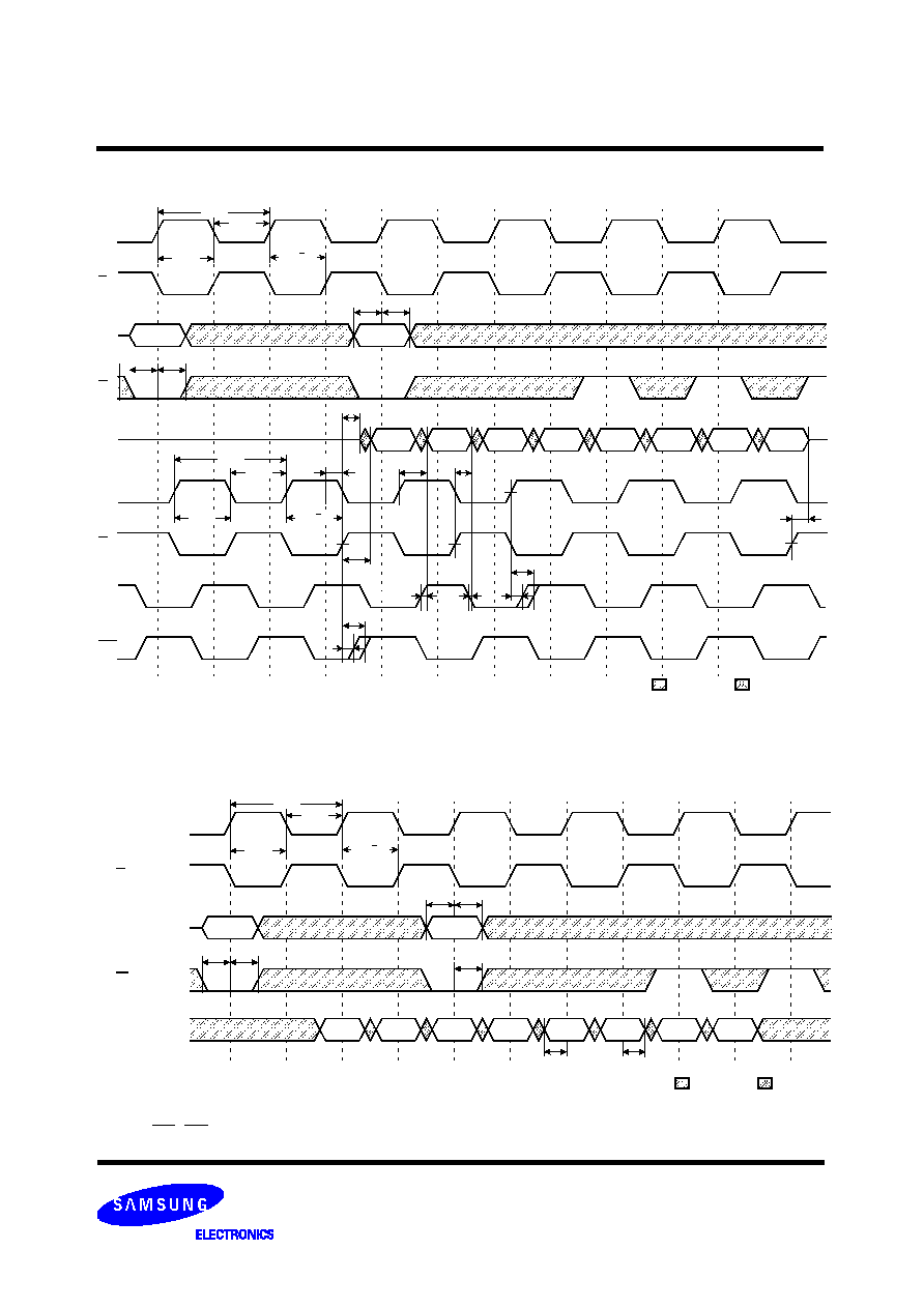
t
KLKH
t
KHKH
t
KHKH
t
KHKL
t
AVKH
t
KHAX
A1
A2
t
IVKH
t
KHIX
Q1-1
Q1-2
Q1-3
Q1-4
Q2-3
t
CHQX
1
t
KHCH
t
CHQV
t
CHQX
t
CQHQV
t
CQHQX
t
CHCQX
t
CHCQV
t
CHQV
t
CHCQX
t
CHCQV
t
KLKH
t
KHKH
t
KHKL
t
KHKH
Note: 1. Q1-1 refers to output from address A1+0, Q1-2 refers to output from address A1+1 i.e. the next internal burst address following A1+0.
2. Outputs are disabled one cycle after a NOP.
K
SA
R
K
Q
C
C
TIMING WAVE FORMS OF READ AND NOP
Don
t Care Undefined
CQ
CQ
Q2-1
Q2-2
D1-1
D1-2
D1-3
D1-4
K
SA
W
K
D(Data In)
TIMING WAVE FORMS OF WRITE AND NOP
D2-1
D2-2
t
DVKH
t
KHDX
Don
t Care Undefined
Note: 1. D1-1 refers to input to address A1+0, D1-2 refers to input to address A1+1, i.e the next internal burst address following A1+0.
2. BWx ( NWx ) assumed active.
t
KLKH
t
KHKH
t
KHKH
t
KHKL
t
AVKH
t
KHAX
A1
A2
t
IVKH
t
KHIX
D2-3
D2-4
t
KHIX
(Data Out)
Q2-4
t
CHQZ
READ
NOP
NOP
READ
WRITE
NOP
NOP
WRITE
- 14 -
Rev 3.1
July. 2004
512Kx36 & 1Mx18 QDR
TM
II b4 SRAM
K7R163684B
K7R161884B
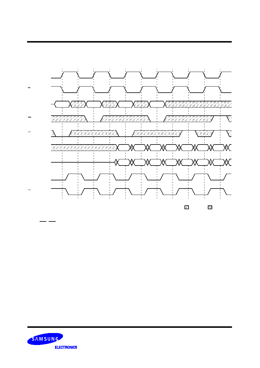
A1
A2
TIMING WAVE FORMS OF READ, WRITE AND NOP
Don
t Care Undefined
Note: 1. If address A3=A2, data Q3-1=D2-1, data Q3-2=D2-2 , data Q3-3=D2-3, data Q3-4=D2-4
Write data is forwarded immediately as read results.
2.BWx ( NWx ) assumed active.
K
SA
W
K
C
C
R
D(Data In)
D(Data Out)
A3
D4-3
D4-2
D4-1
D2-4
D2-3
D2-2
D2-1
A4
Q3-3
Q3-2
Q3-1
Q1-4
Q1-3
Q1-2
Q1-1
READ
NOP
NOP
READ
WRITE
WRITE
- 15 -
Rev 3.1
July. 2004
512Kx36 & 1Mx18 QDR
TM
II b4 SRAM
K7R163684B
K7R161884B
IEEE 1149.1 TEST ACCESS PORT AND BOUNDARY SCAN-JTAG
This part contains an IEEE standard 1149.1 Compatible Test Access Port(TAP). The package pads are monitored by the Serial Scan
circuitry when in test mode. This is to support connectivity testing during manufacturing and system diagnostics. Internal data is not
driven out of the SRAM under JTAG control. In conformance with IEEE 1149.1, the SRAM contains a TAP controller, Instruction Reg-
ister, Bypass Register and ID register. The TAP controller has a standard 16-state machine that resets internally upon power-up,
therefore, TRST signal is not required. It is possible to use this device without utilizing the TAP. To disable the TAP controller without
interfacing with normal operation of the SRAM, TCK must be tied to V
SS
to preclude mid level input. TMS and TDI are designed so an
undriven input will produce a response identical to the application of a logic 1, and may be left unconnected. But they may also be
tied to V
DD
through a resistor. TDO should be left unconnected.
TAP Controller State Diagram
JTAG Block Diagram
Test Logic Reset
Run Test Idle
0
1
1
1
1
0
0
0
1
0
1
1
0
0
0
1
0
1
1
1
0
0
0
0
0
0
0
Select DR
Capture DR
Shift DR
Exit1 DR
Pause DR
Exit2 DR
Update DR
Select IR
Capture IR
Shift IR
Exit1 IR
Pause IR
Exit2 IR
Update IR
1
1
1
1
1
JTAG Instruction Coding
NOTE :
1. Places DQs in Hi-Z in order to sample all input data regardless of other
SRAM inputs. This instruction is not IEEE 1149.1 compliant.
2. Places DQs in Hi-Z in order to sample all input data regardless of other
SRAM inputs.
3. TDI is sampled as an input to the first ID register to allow for the serial shift
of the external TDI data.
4. Bypass register is initiated to V
SS
when BYPASS instruction is invoked. The
Bypass Register also holds serially loaded TDI when exiting the Shift DR
states.
5. SAMPLE instruction dose not places DQs in Hi-Z.
6. This instruction is reserved for future use.
IR2 IR1 IR0
Instruction
TDO Output
Notes
0
0
0
EXTEST
Boundary Scan Register
1
0
0
1
IDCODE
Identification Register
3
0
1
0
SAMPLE-Z
Boundary Scan Register
2
0
1
1
RESERVED Do Not Use
6
1
0
0
SAMPLE
Boundary Scan Register
5
1
0
1
RESERVED Do Not Use
6
1
1
0
RESERVED Do Not Use
6
1
1
1
BYPASS
Bypass Register
4
SRAM
CORE
BYPASS Reg.
Identification Reg.
Instruction Reg.
Control Signals
TAP Controller
TDO
TDI
TMS
TCK
CQ
K,K
C,C
A,D
Q
CQ
- 16 -
Rev 3.1
July. 2004
512Kx36 & 1Mx18 QDR
TM
II b4 SRAM
K7R163684B
K7R161884B
ID REGISTER DEFINITION
Note : Part Configuration
/def=001 for 18Mb, /wx=11 for x36, 10 for x18
/t=1 for DLL Ver., 0 for non-DLL Ver. /q=1 for QDR, 0 for DDR /b=1 for 4Bit Burst, 0 for 2Bit Burst /s=1 for Separate I/O, 0 for Common I/O
Part
Revision Number
(31:29)
Part Configuration
(28:12)
Samsung JEDEC Code
(11: 1)
Start Bit(0)
512Kx36
000
00def0wx0t0q0b0s0
00001001110
1
1Mx18
000
00def0wx0t0q0b0s0
00001001110
1
SCAN REGISTER DEFINITION
Part
Instruction Register
Bypass Register
ID Register
Boundary Scan
512Kx36
3 bits
1 bit
32 bits
107 bits
1Mx18
3 bits
1 bit
32 bits
107 bits
Note: 1. NC pins are read as "X" ( i.e. don
t care.)
ORDER
PIN ID
37
10D
38
9E
39
10C
40
11D
41
9C
42
9D
43
11B
44
11C
45
9B
46
10B
47
11A
48
Internal
49
9A
50
8B
51
7C
52
6C
53
8A
54
7A
55
7B
56
6B
57
6A
58
5B
59
5A
60
4A
61
5C
62
4B
63
3A
64
1H
65
1A
66
2B
67
3B
68
1C
69
1B
70
3D
71
3C
72
1D
ORDER
PIN ID
73
2C
74
3E
75
2D
76
2E
77
1E
78
2F
79
3F
80
1G
81
1F
82
3G
83
2G
84
1J
85
2J
86
3K
87
3J
88
2K
89
1K
90
2L
91
3L
92
1M
93
1L
94
3N
95
3M
96
1N
97
2M
98
3P
99
2N
100
2P
101
1P
102
3R
103
4R
104
4P
105
5P
106
5N
107
5R
ORDER
PIN ID
1
6R
2
6P
3
6N
4
7P
5
7N
6
7R
7
8R
8
8P
9
9R
10
11P
11
10P
12
10N
13
9P
14
10M
15
11N
16
9M
17
9N
18
11L
19
11M
20
9L
21
10L
22
11K
23
10K
24
9J
25
9K
26
10J
27
11J
28
11H
29
10G
30
9G
31
11F
32
11G
33
9F
34
10F
35
11E
36
10E
BOUNDARY SCAN EXIT ORDER

- 17 -
Rev 3.1
July. 2004
512Kx36 & 1Mx18 QDR
TM
II b4 SRAM
K7R163684B
K7R161884B
JTAG DC OPERATING CONDITIONS
Note: 1. The input level of SRAM pin is to follow the SRAM DC specification
.
Parameter
Symbol
Min
Typ
Max
Unit
Note
Power Supply Voltage
V
DD
1.7
1.8
1.9
V
Input High Level
V
IH
1.3
-
V
DD
+0.3
V
Input Low Level
V
IL
-0.3
-
0.5
V
Output High Voltage(I
OH
=-2mA)
V
OH
1.4
-
V
DD
V
Output Low Voltage(I
OL
=2mA)
V
OL
V
SS
-
0.4
V
JTAG TIMING DIAGRAM
JTAG AC Characteristics
Parameter
Symbol
Min
Max
Unit
Note
TCK Cycle Time
t
CHCH
50
-
ns
TCK High Pulse Width
t
CHCL
20
-
ns
TCK Low Pulse Width
t
CLCH
20
-
ns
TMS Input Setup Time
t
MVCH
5
-
ns
TMS Input Hold Time
t
CHMX
5
-
ns
TDI Input Setup Time
t
DVCH
5
-
ns
TDI Input Hold Time
t
CHDX
5
-
ns
SRAM Input Setup Time
t
SVCH
5
-
ns
SRAM Input Hold Time
t
CHSX
5
-
ns
Clock Low to Output Valid
t
CLQV
0
10
ns
JTAG AC TEST CONDITIONS
Note: 1. See SRAM AC test output load on page 11.
Parameter
Symbol
Min
Unit
Note
Input High/Low Level
V
IH
/V
IL
1.8/0.0
V
Input Rise/Fall Time
TR/TF
1.0/1.0
ns
Input and Output Timing Reference Level
0.9
V
1
TCK
TMS
TDI
PI
t
CHCH
t
MVCH
t
CHMX
t
CHCL
t
CLCH
t
DVCH
t
CHDX
t
CLQV
TDO
(SRAM)
t
SVCH
t
CHSX

- 18 -
Rev 3.1
July. 2004
512Kx36 & 1Mx18 QDR
TM
II b4 SRAM
K7R163684B
K7R161884B
165 FBGA PACKAGE DIMENSIONS
Side View
13mm x 15mm Body, 1.0mm Bump Pitch, 11x15 Ball Array
Bottom View
Top View
Symbol
Value
Units
Note
Symbol
Value
Units
Note
A
13
± 0.1
mm
E