
FLASH MEMORY
K8D6x16UTM / K8D6x16UBM
Revision 1.5
March 2005
1
Document Title
64M Bit (8M x8/4M x16) Dual Bank NOR Flash Memory
Revision History
Revision No.
0.0
1.0
1.1
1.2
1.3
1.4
1.5
Remark
Preliminary
Final
History
Initial Draft
Final Specification
Revised
- Release the stand-by current from typ. 5uA(max. 18uA) to typ.
10uA(max. 30uA).
Not support 48TSOP1 Package
Not support 16M/16M BANK partition
Support 48TSOP1 Package
Support 48TSOP1 Lead Free Package
Support 48FBGA Leaded/Lead Free Package
Draft Date
January 10, 2002
May 22, 2002
June 18, 2003
November 18, 2003
July 22, 2004
September 16,
2004
March 16, 2005

FLASH MEMORY
K8D6x16UTM / K8D6x16UBM
Revision 1.5
March 2005
2
64M Bit (8M x8/4M x16) Dual Bank NOR Flash Memory
The K8D6316U featuring single 3.0V power supply, is a 64Mbit
NOR-type Flash Memory organized as 8Mx8 or 4M x16. The
memory architecture of the device is designed to divide its
memory arrays into 135 blocks to be protected by the block
group. This block architecture provides highly flexible erase and
program capability. The K8D6316U NOR Flash consists of two
banks. This device is capable of reading data from one bank
while programming or erasing in the other bank. Access times
of 70ns, 80ns and 90ns are available for the device. The
device
s fast access times allow high speed microprocessors to
operate without wait states. The device performs a program
operation in units of 8 bits (Byte) or 16 bits (Word) and erases in
units of a block. Single or multiple blocks can be erased. The
block erase operation is completed within typically 0.7 sec. The
device requires 15mA as program/erase current in the standard
and industrial temperature ranges.
The K8D6316U NOR Flash Memory is created by using Sam-
sung's advanced CMOS process technology. This device is
available in 48 pin TSOP1 and 48 ball TBGA,FBGA packages.
The device is compatible with EPROM applications to require
high-density and cost-effective nonvolatile read/write storage
solutions.
FEATURES
∑
Single Voltage, 2.7V to 3.6V for Read and Write operations
∑
Organization
8,388,608 x 8 bit (Byte mode) / 4,194,304 x 16 bit (Word mode)
∑
Fast Read Access Time : 70ns
∑
Read While Program/Erase Operation
∑
Dual Bank architectures
Bank 1 / Bank 2 : 16Mb / 48Mb
∑
Secode(Security Code) Block : Extra 64K Byte block
∑
Power Consumption (typical value @5MHz)
- Read Current : 14mA
- Program/Erase Current : 15mA
- Read While Program or Read While Erase Current : 25mA
- Standby Mode/Auto Sleep Mode : 10
µ
A
∑
WP/ACC input pin
- Allows special protection of two outermost boot blocks at V
IL
,
regardless of block protect status
- Removes special protection of two outermost boot block at V
IH,
the two blocks return to normal block protect status
- Program time at V
HH
: 9
µ
s/word
∑
Erase Suspend/Resume
∑
Unlock Bypass Program
∑
Hardware RESET Pin
∑
Command Register Operation
∑
Block Group Protection / Unprotection
∑
Supports Common Flash Memory Interface
∑
Industrial Temperature : -40
∞
C to 85
∞
C
∑
Endurance : 100,000 Program/Erase Cycles Minimum
∑
Data Retention : 10 years
∑
Package : 48 Pin TSOP1 : 12 x 20 mm / 0.5 mm Pin pitch
48 Ball TBGA :
6 x 9 mm / 0.8 mm Ball pitch
48 Ball FBGA :
6 x 9 mm / 0.8 mm Ball pitch
GENERAL DESCRIPTION
SAMSUNG ELECTRONICS CO., LTD. reserves the right to change products and specifications without notice.
PIN DESCRIPTION
Pin Name
Pin Function
A0 - A21
Address Inputs
DQ0 - DQ14
Data Inputs / Outputs
DQ15/A-1
DQ15 Data Input / Output
A-1 LSB Address
BYTE
Word / Byte Selection
CE
Chip Enable
OE
Output Enable
RESET
Hardware Reset Pin
RY/BY
Ready/Busy Output
WE
Write Enable
WP/ACC
Hardware Write Protection/Program
Acceleration
Vcc
Power Supply
V
SS
Ground
N.C
No Connection
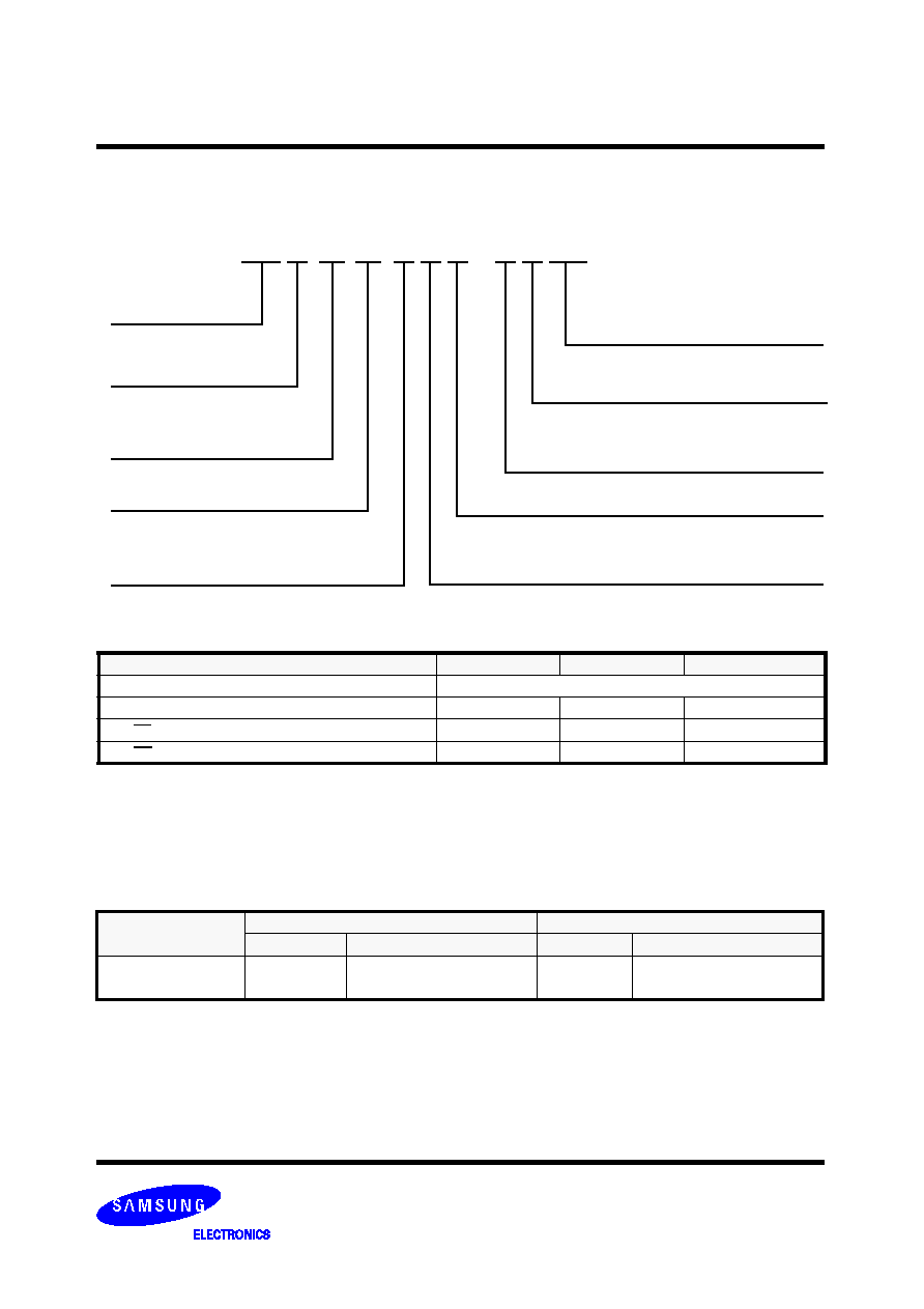
PIN CONFIGURATION
48-pin TSOP1
Standard Type
12mm x 20mm
1
2
3
4
5
6
7
8
9
10
11
12
13
14
15
16
17
18
19
20
21
22
23
24
48
47
46
45
44
43
42
41
40
39
38
37
36
35
34
33
32
31
30
29
28
27
26
25
A15
A14
A13
A12
A11
A10
A9
A8
A19
A20
WE
RESET
A21
WP/ACC
RY/BY
A18
A17
A7
A6
A5
A4
A3
A2
A1
A16
BYTE
Vss
DQ15/A-1
DQ7
DQ14
DQ6
DQ13
DQ5
DQ12
DQ4
Vcc
DQ11
DQ3
DQ10
DQ2
DQ9
DQ1
DQ8
DQ0
OE
Vss
CE
A0
Note :
Please refer to the package dimension.
FLASH MEMORY
K8D6x16UTM / K8D6x16UBM
Revision 1.5
March 2005
3
A3
A7
A9
A13
A4
A17
RESET
RY/BY
A8
A12
A2
A6
A18
A21
A10
A14
DQ15/
A5
A20
A19
A11
A0
DQ0
DQ2
DQ5
DQ7
A16
CE
DQ8
DQ10
DQ12
DQ14
BYTE
DQ9
DQ11
V
CC
DQ13
V
SS
DQ1
DQ3
DQ4
DQ6
V
SS
A-1
2
3
4
5
6
C
D
E
F
G
H
WE
WP/
A1
A15
OE
ACC
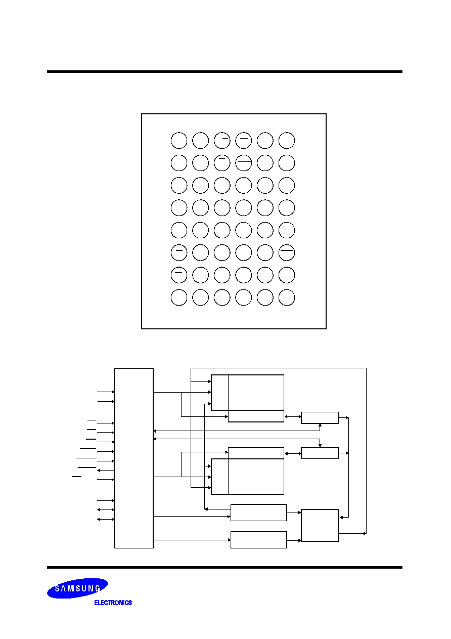
FUNCTIONAL BLOCK DIAGRAM
Vcc
Vss
CE
OE
WE
BYTE
RESET
RY/BY
A0~A21
DQ0~DQ14
I/O
Interface
&
Bank
Control
X
Dec
Y Dec
Latch &
Control
Latch &
Control
Dec
X
Y Dec
Erase
Control
Program
Control
High
Voltage
Gen.
Bank2
Cell Array
Bank1
Address
Bank2
Address
Bank1 Data-In/Out
Bank2 Data-In/Out
Bank1
Cell Array
48 Ball TBGA/FBGA TOP VIEW (BALL DOWN)
1
A
B
WP/ACC
DQ15/A-1
FLASH MEMORY
K8D6x16UTM / K8D6x16UBM
Revision 1.5
March 2005
4
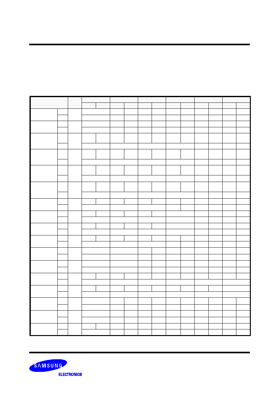
Table 2. K8D6316U DEVICE BANK DIVISIONS
Device
Part Number
Bank 1
Bank 2
Mbit
Block Sizes
Mbit
Block Sizes
K8D6316U
16 Mbit
Eight 8 Kbyte/4 Kword,
thirty-one 64 Kbyte/32 Kword
48 Mbit
Ninety-six
64 Kbyte/32 Kword
ORDERING INFORMATION
K 8 D 6x 1 6 U T M - T I 0 7
Samsung
NOR Flash Memory
Device Type
Dual Bank Boot Block
Bank Division
63 = 16Mbits + 48Mbits
Operating Temperature Range
C = Commercial Temp. (0
∞
C to 70
∞
C)
I = Industrial Temp. (-40
∞
C to 85
∞
C)
Block Architecture
T = Top Boot Block
B = Bottom Boot Block
Version
M = 1st Generation
Access Time
07 = 70 ns
08 = 80 ns
09 = 90 ns
Operating Voltage Range
2.7V to 3.6V
Organization
x8/x16 Selectable
Table 1. PRODUCT LINE-UP
Part No.
- 7
-8
-9
Vcc
2.7V~3.6V
Max. Address Access Time (ns)
70ns
80ns
90ns
Max. CE Access Time (ns)
70ns
80ns
90ns
Max. OE Access Time (ns)
25ns
25ns
35ns
Package
P = 48TSOP1(Lead-Free) Y = 48 TSOP1
D : FBGA(Lead Free) F : FBGA
L : TBGA(Lead Free) T : TBGA
FLASH MEMORY
K8D6x16UTM / K8D6x16UBM
Revision 1.5
March 2005
5
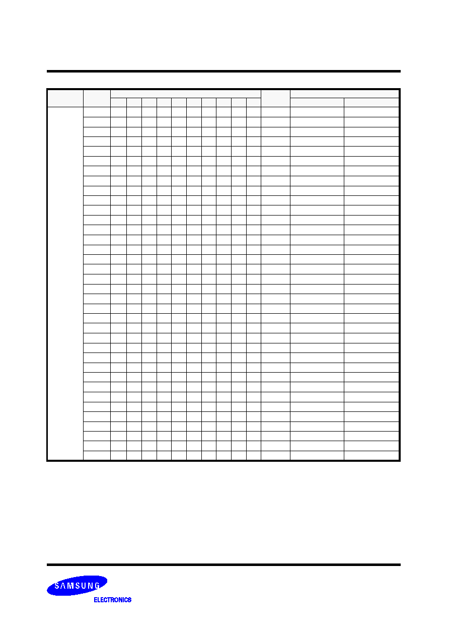
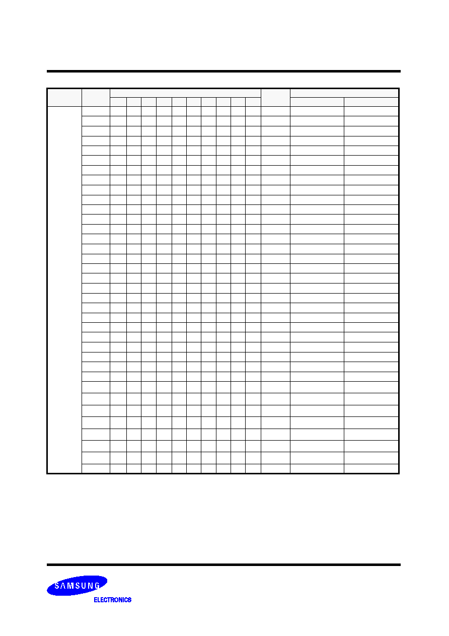
Table 3. Top Boot
Block Address (K8D6316UT)
K8D6316UT
Block
Block Address
Block Size
(KB/KW)
Address Range
A21
A20
A19
A18
A17
A16
A15
A14
A13
A12
Byte Mode
Word Mode
Bank1
BA134
1
1
1
1
1
1
1
1
1
1
8/4
7FE000H-7FFFFFH
3FF000H-3FFFFFH
BA133
1
1
1
1
1
1
1
1
1
0
8/4
7FC000H-7FDFFFH
3FE000H-3FEFFFH
BA132
1
1
1
1
1
1
1
1
0
1
8/4
7FA000H-7FBFFFH
3FD000H-3FDFFFH
BA131
1
1
1
1
1
1
1
1
0
0
8/4
7F8000H-7F9FFFH
3FC000H-3FCFFFH
BA130
1
1
1
1
1
1
1
0
1
1
8/4
7F6000H-7F7FFFH
3FB000H-3FBFFFH
BA129
1
1
1
1
1
1
1
0
1
0
8/4
7F4000H-7F5FFFH
3FA000H-3FAFFFH
BA128
1
1
1
1
1
1
1
0
0
1
8/4
7F2000H-7F3FFFH
3F9000H-3F9FFFH
BA127
1
1
1
1
1
1
1
0
0
0
8/4
7F0000H-7F1FFFH
3F8000H-3F8FFFH
BA126
1
1
1
1
1
1
0
X
X
X
64/32
7E0000H-7EFFFFH
3F0000H-3F7FFFH
BA125
1
1
1
1
1
0
1
X
X
X
64/32
7D0000H-7DFFFFH
3E8000H-3EFFFFH
BA124
1
1
1
1
1
0
0
X
X
X
64/32
7C0000H-7CFFFFH
3E0000H-3E7FFFH
BA123
1
1
1
1
0
1
1
X
X
X
64/32
7B0000H-7BFFFFH
3D8000H-3DFFFFH
BA122
1
1
1
1
0
1
0
X
X
X
64/32
7A0000H-7AFFFFH
3D0000H-3D7FFFH
BA121
1
1
1
1
0
0
1
X
X
X
64/32
790000H-79FFFFH
3C8000H-3CFFFFH
BA120
1
1
1
1
0
0
0
X
X
X
64/32
780000H-78FFFFH
3C0000H-3C7FFFH
BA119
1
1
1
0
1
1
1
X
X
X
64/32
770000H-77FFFFH
3B8000H-3BFFFFH
BA118
1
1
1
0
1
1
0
X
X
X
64/32
760000H-76FFFFH
3B0000H-3B7FFFH
BA117
1
1
1
0
1
0
1
X
X
X
64/32
750000H-75FFFFH
3A8000H-3AFFFFH
BA116
1
1
1
0
1
0
0
X
X
X
64/32
740000H-74FFFFH
3A0000H-3A7FFFH
BA115
1
1
1
0
0
1
1
X
X
X
64/32
730000H-73FFFFH
398000H-39FFFFH
BA114
1
1
1
0
0
1
0
X
X
X
64/32
720000H-72FFFFH
390000H-397FFFH
BA113
1
1
1
0
0
0
1
X
X
X
64/32
710000H-71FFFFH
388000H-38FFFFH
BA112
1
1
1
0
0
0
0
X
X
X
64/32
700000H-70FFFFH
380000H-387FFFH
BA111
1
1
0
1
1
1
1
X
X
X
64/32
6F0000H-6FFFFFH
378000H-37FFFFH
BA110
1
1
0
1
1
1
0
X
X
X
64/32
6E0000H-6EFFFFH
370000H-377FFFH
BA109
1
1
0
1
1
0
1
X
X
X
64/32
6D0000H-6DFFFFH
368000H-36FFFFH
BA108
1
1
0
1
1
0
0
X
X
X
64/32
6C0000H-6CFFFFH
360000H-367FFFH
BA107
1
1
0
1
0
1
1
X
X
X
64/32
6B0000H-6BFFFFH
358000H-35FFFFH
BA106
1
1
0
1
0
1
0
X
X
X
64/32
6A0000H-6AFFFFH
350000H-357FFFH
BA105
1
1
0
1
0
0
1
X
X
X
64/32
690000H-69FFFFH
348000H-34FFFFH
BA104
1
1
0
1
0
0
0
X
X
X
64/32
680000H-68FFFFH
340000H-347FFFH
BA103
1
1
0
0
1
1
1
X
X
X
64/32
670000H-67FFFFH
338000H-33FFFFH
BA102
1
1
0
0
1
1
0
X
X
X
64/32
660000H-66FFFFH
330000H-337FFFH
BA101
1
1
0
0
1
0
1
X
X
X
64/32
650000H-65FFFFH
328000H-32FFFFH
BA100
1
1
0
0
1
0
0
X
X
X
64/32
640000H-64FFFFH
320000H-327FFFH
BA99
1
1
0
0
0
1
1
X
X
X
64/32
630000H-63FFFFH
318000H-31FFFFH

FLASH MEMORY
K8D6x16UTM / K8D6x16UBM
Revision 1.5
March 2005
6
Table 3. Top Boot Block Address (Continued)
K8D6316UT
Block
Block Address
Block Size
(KB/KW)
Address Range
A21
A20
A19
A18
A17
A16
A15
A14
A13
A12
Byte Mode
Word Mode
Bank1
BA98
1
1
0
0
0
1
0
X
X
X
64/32
620000H-62FFFFH
310000H-317FFFH
BA97
1
1
0
0
0
0
1
X
X
X
64/32
610000H-61FFFFH
308000H-30FFFFH
BA96
1
1
0
0
0
0
0
X
X
X
64/32
600000H-60FFFFH
300000H-307FFFH
Bank2
BA95
1
0
1
1
1
1
1
X
X
X
64/32
5F0000H-5FFFFFH
2F8000H-2FFFFFH
BA94
1
0
1
1
1
1
0
X
X
X
64/32
5E0000H-5EFFFFH
2F0000H-2F7FFFH
BA93
1
0
1
1
1
0
1
X
X
X
64/32
5D0000H-5DFFFFH
2E8000H-2EFFFFH
BA92
1
0
1
1
1
0
0
X
X
X
64/32
5C0000H-5CFFFFH
2E0000H-2E7FFFH
BA91
1
0
1
1
0
1
1
X
X
X
64/32
5B0000H-5BFFFFH
2D8000H-2DFFFFH
BA90
1
0
1
1
0
1
0
X
X
X
64/32
5A0000H-5AFFFFH
2D0000H-2D7FFFH
BA89
1
0
1
1
0
0
1
X
X
X
64/32
590000H-59FFFFH
2C8000H20CFFFFH
BA88
1
0
1
1
0
0
0
X
X
X
64/32
580000H-58FFFFH
2C0000H-2C7FFFH
BA87
1
0
1
0
1
1
1
X
X
X
64/32
570000H-57FFFFH
2B8000H-2BFFFFH
BA86
1
0
1
0
1
1
0
X
X
X
64/32
560000H-56FFFFH
2B0000H-2B7FFFH
BA85
1
0
1
0
1
0
1
X
X
X
64/32
550000H-55FFFFH
2A8000H-2AFFFFH
BA84
1
0
1
0
1
0
0
X
X
X
64/32
540000H-54FFFFH
2A0000H-2A7FFFH
BA83
1
0
1
0
0
1
1
X
X
X
64/32
530000H-53FFFFH
298000H-29FFFFH
BA82
1
0
1
0
0
1
0
X
X
X
64/32
520000H-52FFFFH
290000H-297FFFH
BA81
1
0
1
0
0
0
1
X
X
X
64/32
510000H-51FFFFH
288000H-28FFFFH
BA80
1
0
1
0
0
0
0
X
X
X
64/32
500000H-50FFFFH
280000H-287FFFH
BA79
1
0
0
1
1
1
1
X
X
X
64/32
4F0000H-4FFFFFH
278000H-27FFFFH
BA78
1
0
0
1
1
1
0
X
X
X
64/32
4E0000H-4EFFFFH
270000H-277FFFH
BA77
1
0
0
1
1
0
1
X
X
X
64/32
4D0000H-4DFFFFH
268000H-26FFFFH
BA76
1
0
0
1
1
0
0
X
X
X
64/32
4C0000H-4CFFFFH
260000H-267FFFH
BA75
1
0
0
1
0
1
1
X
X
X
64/32
4B0000H-4BFFFFH
258000H-25FFFFH
BA74
1
0
0
1
0
1
0
X
X
X
64/32
4A0000H-4AFFFFH
250000H-257FFFH
BA73
1
0
0
1
0
0
1
X
X
X
64/32
490000H-49FFFFH
248000H-24FFFFH
BA72
1
0
0
1
0
0
0
X
X
X
64/32
480000H-48FFFFH
240000H-247FFFH
BA71
1
0
0
0
1
1
1
X
X
X
64/32
470000H-47FFFFH
238000H-23FFFFH

FLASH MEMORY
K8D6x16UTM / K8D6x16UBM
Revision 1.5
March 2005
7
Table 3. Top Boot
Block Address (Continued)
K8D6316UT
Block
Block Address
Block Size
(KB/KW)
Address Range
A21
A20
A19
A18
A17
A16
A15
A14
A13
A12
Byte Mode
Word Mode
Bank2
BA70
1
0
0
0
1
1
0
X
X
X
64/32
460000H-46FFFFH
230000H-237FFFH
BA69
1
0
0
0
1
0
1
X
X
X
64/32
450000H-45FFFFH
228000H-22FFFFH
BA68
1
0
0
0
1
0
0
X
X
X
64/32
440000H-44FFFFH
220000H-227FFFH
BA67
1
0
0
0
0
1
1
X
X
X
64/32
430000H-43FFFFH
218000H-21FFFFH
BA66
1
0
0
0
0
1
0
X
X
X
64/32
420000H-42FFFFH
210000H-217FFFH
BA65
1
0
0
0
0
0
1
X
X
X
64/32
410000H-41FFFFH
208000H-20FFFFH
BA64
1
0
0
0
0
0
0
X
X
X
64/32
400000H-3FFFFFH
200000H-207FFFH
BA63
0
1
1
1
1
1
1
X
X
X
64/32
3F0000H-3FFFFFH
1F8000H-1FFFFFH
BA62
0
1
1
1
1
1
0
X
X
X
64/32
3E0000H-3EFFFFH
1F0000H-1F7FFFH
BA61
0
1
1
1
1
0
1
X
X
X
64/32
3D0000H-3DFFFFH
1E8000H-1EFFFFH
BA60
0
1
1
1
1
0
0
X
X
X
64/32
3C0000H-3CFFFFH
1E0000H-1E7FFFH
BA59
0
1
1
1
0
1
1
X
X
X
64/32
3B0000H-3BFFFFH
1D8000H-1DFFFFH
BA58
0
1
1
1
0
1
0
X
X
X
64/32
3A0000H-3AFFFFH
1D0000H-1D7FFFH
BA57
0
1
1
1
0
0
1
X
X
X
64/32
390000H-39FFFFH
1C8000H-1CFFFFH
BA56
0
1
1
1
0
0
0
X
X
X
64/32
380000H-38FFFFH
1C0000H-1C7FFFH
BA55
0
1
1
0
1
1
1
X
X
X
64/32
370000H-37FFFFH
1B8000H-1BFFFFH
BA54
0
1
1
0
1
1
0
X
X
X
64/32
360000H-36FFFFH
1B0000H-1B7FFFH
BA53
0
1
1
0
1
0
1
X
X
X
64/32
350000H-35FFFFH
1A8000H-1AFFFFH
BA52
0
1
1
0
1
0
0
X
X
X
64/32
340000H-34FFFFH
1A0000H-1A7FFFH
BA51
0
1
1
0
0
1
1
X
X
X
64/32
330000H-33FFFFH
198000H-19FFFFH
BA50
0
1
1
0
0
1
0
X
X
X
64/32
320000H-32FFFFH
190000H-197FFFH
BA49
0
1
1
0
0
0
1
X
X
X
64/32
310000H-31FFFFH
188000H-18FFFFH
BA48
0
1
1
0
0
0
0
X
X
X
64/32
300000H-30FFFFH
180000H-187FFFH
BA47
0
1
0
1
1
1
1
X
X
X
64/32
2F0000H-2FFFFFH
178000H-17FFFFH
BA46
0
1
0
1
1
1
0
X
X
X
64/32
2E0000H-2EFFFFH
170000H-177FFFH
BA45
0
1
0
1
1
0
1
X
X
X
64/32
2D0000H-2DFFFFH
168000H-16FFFFH
BA44
0
1
0
1
1
0
0
X
X
X
64/32
2C0000H-2CFFFFH
160000H-167FFFH
BA43
0
1
0
1
0
1
1
X
X
X
64/32
2B0000H-2BFFFFH
158000H-15FFFFH
BA42
0
1
0
1
0
1
0
X
X
X
64/32
2A0000H-2AFFFFH
150000H-157FFFH
BA41
0
1
0
1
0
0
1
X
X
X
64/32
290000H-29FFFFH
148000H-14FFFFH
BA40
0
1
0
1
0
0
0
X
X
X
64/32
280000H-28FFFFH
140000H-147FFFH
BA39
0
1
0
0
1
1
1
X
X
X
64/32
270000H-27FFFFH
138000H-13FFFFH
BA38
0
1
0
0
1
1
0
X
X
X
64/32
260000H-26FFFFH
130000H-137FFFH
BA37
0
1
0
0
1
0
1
X
X
X
64/32
250000H-25FFFFH
128000H-12FFFFH
BA36
0
1
0
0
1
0
0
X
X
X
64/32
240000H-24FFFFH
120000H-127FFFH
BA35
0
1
0
0
0
1
1
X
X
X
64/32
230000H-23FFFFH
118000H-11FFFFH
FLASH MEMORY
K8D6x16UTM / K8D6x16UBM
Revision 1.5
March 2005
8
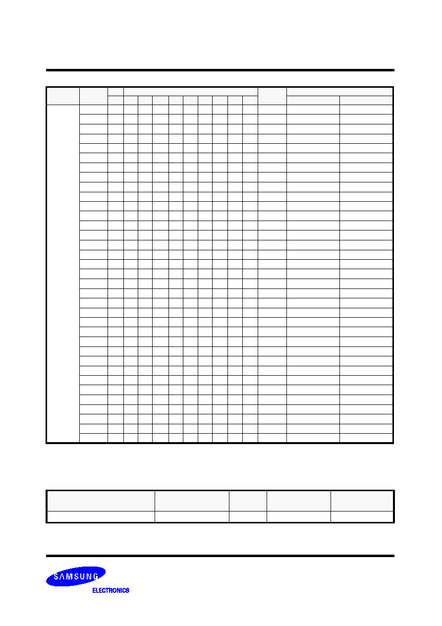
Table 3. Top Boot Block Address (Continued)
Note :
The bank address bits are A21
A20 for K8D6316UT.
K8D6316UT
Block
Block Address
Block Size
(KB/KW)
Address Range
A21
A20
A19
A18
A17
A16
A15
A14
A13
A12
Byte Mode
Word Mode
Bank2
BA34
0
1
0
0
0
1
0
X
X
X
64/32
220000H-22FFFFH
110000H-117FFFH
BA33
0
1
0
0
0
0
1
X
X
X
64/32
210000H-21FFFFH
108000H-10FFFFH
BA32
0
1
0
0
0
0
0
X
X
X
64/32
200000H-20FFFFH
100000H-107FFFH
BA31
0
0
1
1
1
1
1
X
X
X
64/32
1F0000H-1FFFFFH
0F8000H-0FFFFFH
BA30
0
0
1
1
1
1
0
X
X
X
64/32
1E0000H-1EFFFFH
0F0000H-0F7FFFH
BA29
0
0
1
1
1
0
1
X
X
X
64/32
1D0000H-1DFFFFH
0E8000H-0EFFFFH
BA28
0
0
1
1
1
0
0
X
X
X
64/32
1C0000H-1CFFFFH
0E0000H-0E7FFFH
BA27
0
0
1
1
0
1
1
X
X
X
64/32
1B0000H-1BFFFFH
0D8000H-0DFFFFH
BA26
0
0
1
1
0
1
0
X
X
X
64/32
1A0000H-1AFFFFH
0D0000H-0D7FFFH
BA25
0
0
1
1
0
0
1
X
X
X
64/32
190000H-19FFFFH
0C8000H-0CFFFFH
BA24
0
0
1
1
0
0
0
X
X
X
64/32
180000H-18FFFFH
0C0000H-0C7FFFH
BA23
0
0
1
0
1
1
1
X
X
X
64/32
170000H-17FFFFH
0B8000H-0BFFFFH
BA22
0
0
1
0
1
1
0
X
X
X
64/32
160000H-16FFFFH
0B0000H-0B7FFFH
BA21
0
0
1
0
1
0
1
X
X
X
64/32
150000H-15FFFFH
0A8000H-0AFFFFH
BA20
0
0
1
0
1
0
0
X
X
X
64/32
140000H-14FFFFH
0A0000H-0A7FFFH
BA19
0
0
1
0
0
1
1
X
X
X
64/32
130000H-13FFFFH
098000H-09FFFFH
BA18
0
0
1
0
0
1
0
X
X
X
64/32
120000H-12FFFFH
090000H-097FFFH
BA17
0
0
1
0
0
0
1
X
X
X
64/32
110000H-11FFFFH
088000H-08FFFFH
BA16
0
0
1
0
0
0
0
X
X
X
64/32
100000H-10FFFFH
080000H-087FFFH
BA15
0
0
0
1
1
1
1
X
X
X
64/32
0F0000H-0FFFFFH
078000H-07FFFFH
BA14
0
0
0
1
1
1
0
X
X
X
64/32
0E0000H-0EFFFFH
070000H-077FFFH
BA13
0
0
0
1
1
0
1
X
X
X
64/32
0D0000H-0DFFFFH
068000H-06FFFFH
BA12
0
0
0
1
1
0
0
X
X
X
64/32
0C0000H-0CFFFFH
060000H-067FFFH
BA11
0
0
0
1
0
1
1
X
X
X
64/32
0B0000H-0BFFFFH
058000H-05FFFFH
BA10
0
0
0
1
0
1
0
X
X
X
64/32
0A0000H-0AFFFFH
050000H-057FFFH
BA9
0
0
0
1
0
0
1
X
X
X
64/32
090000H-09FFFFH
048000H-04FFFFH
BA8
0
0
0
1
0
0
0
X
X
X
64/32
080000H-08FFFFH
040000H-047FFFH
BA7
0
0
0
0
1
1
1
X
X
X
64/32
070000H-07FFFFH
038000H-03FFFFH
BA6
0
0
0
0
1
1
0
X
X
X
64/32
060000H-06FFFFH
030000H-037FFFH
BA5
0
0
0
0
1
0
1
X
X
X
64/32
050000H-05FFFFH
028000H-02FFFFH
BA4
0
0
0
0
1
0
0
X
X
X
64/32
040000H-04FFFFH
020000H-027FFFH
BA3
0
0
0
0
0
1
1
X
X
X
64/32
030000H-03FFFFH
018000H-01FFFFH
BA2
0
0
0
0
0
1
0
X
X
X
64/32
020000H-02FFFFH
010000H-017FFFH
BA1
0
0
0
0
0
0
1
X
X
X
64/32
010000H-01FFFFH
008000H-00FFFFH
BA0
0
0
0
0
0
0
0
X
X
X
64/32
000000H-00FFFFH
000000H-007FFFH
Device
Block Address
A21-A12
Block Size
(KB/KW)
(X8)
Address Range
(X16)
Address Range
K8D6316UT
1111111xxx
64/32
7F0000H-7FFFFFH
3F8000H-3FFFFFH
Table 4. Secode Block Addresses for Top Boot Devices
FLASH MEMORY
K8D6x16UTM / K8D6x16UBM
Revision 1.5
March 2005
9
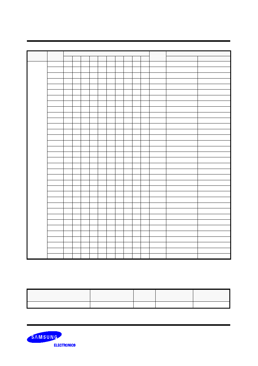
Table 5. Bottom Boot Block Address (K8D6316UB)
K8D6316UB
Block
Block Address
Block Size
(KB/KW)
Address Range
A21
A20
A19
A18
A17
A16
A15
A14
A13
A12
Byte Mode
Word Mode
Bank2
BA134
1
1
1
1
1
1
1
X
X
X
64/32
7F0000H-7FFFFFH
3F8000H-3FFFFFH
BA133
1
1
1
1
1
1
0
X
X
X
64/32
7E0000H-7EFFFFH
3F0000H-3F7FFFH
BA132
1
1
1
1
1
0
1
X
X
X
64/32
7D0000H-7DFFFFH
3E8000H-3EFFFFH
BA131
1
1
1
1
1
0
0
X
X
X
64/32
7C0000H-7CFFFFH
3E0000H-3E7FFFH
BA130
1
1
1
1
0
1
1
X
X
X
64/32
7B0000H-7BFFFFH
3D8000H-3DFFFFH
BA129
1
1
1
1
0
1
0
X
X
X
64/32
7A0000H-7AFFFFH
3D0000H-3D7FFFH
BA128
1
1
1
1
0
0
1
X
X
X
64/32
790000H-79FFFFH
3C8000H-3CFFFFH
BA127
1
1
1
1
0
0
0
X
X
X
64/32
780000H-78FFFFH
3C0000H-3C7FFFH
BA126
1
1
1
0
1
1
1
X
X
X
64/32
770000H-77FFFFH
3B8000H-3BFFFFH
BA125
1
1
1
0
1
1
0
X
X
X
64/32
760000H-76FFFFH
3B0000H-3B7FFFH
BA124
1
1
1
0
1
0
1
X
X
X
64/32
750000H-75FFFFH
3A8000H-3AFFFFH
BA123
1
1
1
0
1
0
0
X
X
X
64/32
740000H-74FFFFH
3A0000H-3A7FFFH
BA122
1
1
1
0
0
1
1
X
X
X
64/32
730000H-73FFFFH
398000H-39FFFFH
BA121
1
1
1
0
0
1
0
X
X
X
64/32
720000H-72FFFFH
390000H-397FFFH
BA120
1
1
1
0
0
0
1
X
X
X
64/32
710000H-71FFFFH
388000H-38FFFFH
BA119
1
1
1
0
0
0
0
X
X
X
64/32
700000H-70FFFFH
380000H-387FFFH
BA118
1
1
0
1
1
1
1
X
X
X
64/32
6F0000H-6F1FFFH
378000H-37FFFFH
BA117
1
1
0
1
1
1
0
X
X
X
64/32
6E0000H-6EFFFFH
370000H-377FFFH
BA116
1
1
0
1
1
0
1
X
X
X
64/32
6D0000H-6DFFFFH
368000H-36FFFFH
BA115
1
1
0
1
1
0
0
X
X
X
64/32
6C0000H-6CFFFFH
360000H-367FFFH
BA114
1
1
0
1
0
1
1
X
X
X
64/32
6B0000H-6BFFFFH
358000H-35FFFFH
BA113
1
1
0
1
0
1
0
X
X
X
64/32
6A0000H-6AFFFFH
350000H-357FFFH
BA112
1
1
0
1
0
0
1
X
X
X
64/32
690000H-69FFFFH
348000H-34FFFFH
BA111
1
1
0
1
0
0
0
X
X
X
64/32
680000H-68FFFFH
340000H-347FFFH
BA110
1
1
0
0
1
1
1
X
X
X
64/32
670000H-67FFFFH
338000H-33FFFFH
BA109
1
1
0
0
1
1
0
X
X
X
64/32
660000H-66FFFFH
330000H-337FFFH
BA108
1
1
0
0
1
0
1
X
X
X
64/32
650000H-65FFFFH
328000H-32FFFFH
BA107
1
1
0
0
1
0
0
X
X
X
64/32
640000H-64FFFFH
320000H-327FFFH
BA106
1
1
0
0
0
1
1
X
X
X
64/32
630000H-63FFFFH
318000H-31FFFFH
BA105
1
1
0
0
0
1
0
X
X
X
64/32
620000H-62FFFFH
310000H-317FFFH
BA104
1
1
0
0
0
0
1
X
X
X
64/32
610000H-61FFFFH
308000H-30FFFFH
BA103
1
1
0
0
0
0
0
X
X
X
64/32
600000H-60FFFFH
300000H-307FFFH
BA102
1
0
1
1
1
1
1
X
X
X
64/32
5F0000H-5FFFFFH
2F8000H-2FFFFFH
BA101
1
0
1
1
1
1
0
X
X
X
64/32
5E0000H-5EFFFFH
2F0000H-2F7FFFH
BA100
1
0
1
1
1
0
1
X
X
X
64/32
5D0000H-5DFFFFH
2E8000H-2EFFFFH
BA99
1
0
1
1
1
0
0
X
X
X
64/32
5C0000H-5CFFFFH
2E0000H-2E7FFFH
FLASH MEMORY
K8D6x16UTM / K8D6x16UBM
Revision 1.5
March 2005
10
Table 5. Bottom Block Address (Continued)
K8D6316UB
Block
Block Address
Block Size
(KB/KW)
Address Range
A21
A20
A19
A18
A17
A16
A15
A14
A13
A12
Byte Mode
Word Mode
Bank2
BA98
1
0
1
1
0
1
1
X
X
X
64/32
5B0000H-5BFFFFH
2D8000H-2DFFFFH
BA97
1
0
1
1
0
1
0
X
X
X
64/32
5A0000H-5AFFFFH
2D0000H-2D7FFFH
BA96
1
0
1
1
0
0
1
X
X
X
64/32
590000H-59FFFFH
2C8000H-2CFFFFH
BA95
1
0
1
1
0
0
0
X
X
X
64/32
580000H-58FFFFH
2C0000H-2C7FFFH
BA94
1
0
1
0
1
1
1
X
X
X
64/32
570000H-57FFFFH
2B8000H-2BFFFFH
BA93
1
0
1
0
1
1
0
X
X
X
64/32
560000H-56FFFFH
2B0000H-2B7FFFH
BA92
1
0
1
0
1
0
1
X
X
X
64/32
550000H-55FFFFH
2A8000H-2AFFFFH
BA91
1
0
1
0
1
0
0
X
X
X
64/32
540000H-54FFFFH
2A0000H-2A7FFFH
BA90
1
0
1
0
0
1
1
X
X
X
64/32
530000H-53FFFFH
298000H-29FFFFH
BA89
1
0
1
0
0
1
0
X
X
X
64/32
520000H-52FFFFH
290000H-297FFFH
BA88
1
0
1
0
0
0
1
X
X
X
64/32
510000H-51FFFFH
288000H-28FFFFH
BA87
1
0
1
0
0
0
0
X
X
X
64/32
500000H-50FFFFH
280000H-287FFFH
BA86
1
0
0
1
1
1
1
X
X
X
64/32
4F0000H-4FFFFFH
278000H-27FFFFH
BA85
1
0
0
1
1
1
0
X
X
X
64/32
4E0000H-4EFFFFH
270000H-277FFFH
BA84
1
0
0
1
1
0
1
X
X
X
64/32
4D0000H-4DFFFFH
268000H-26FFFFH
BA83
1
0
0
1
1
0
0
X
X
X
64/32
4C0000H-4CFFFFH
260000H-267FFFH
BA82
1
0
0
1
0
1
1
X
X
X
64/32
4B0000H-4BFFFFH
258000H-25FFFFH
BA81
1
0
0
1
0
1
0
X
X
X
64/32
4A0000H-4AFFFFH
250000H-257FFFH
BA80
1
0
0
1
0
0
1
X
X
X
64/32
490000H-49FFFFH
248000H-24FFFFH
BA79
1
0
0
1
0
0
0
X
X
X
64/32
480000H-48FFFFH
240000H-247FFFH
BA78
1
0
0
0
1
1
1
X
X
X
64/32
470000H-47FFFFH
238000H-23FFFFH
BA77
1
0
0
0
1
1
0
X
X
X
64/32
460000H-46FFFFH
230000H-237FFFH
BA76
1
0
0
0
1
0
1
X
X
X
64/32
450000H-45FFFFH
228000H-22FFFFH
BA75
1
0
0
0
1
0
0
X
X
X
64/32
440000H-44FFFFH
220000H-227FFFH
BA74
1
0
0
0
0
1
1
X
X
X
64/32
430000H-43FFFFH
218000H-21FFFFH
BA73
1
0
0
0
0
1
0
X
X
X
64/32
420000H-42FFFFH
210000H-217FFFH
BA72
1
0
0
0
0
0
1
X
X
X
64/32
410000H-41FFFFH
208000H-20FFFFH
BA71
1
0
0
0
0
0
0
X
X
X
64/32
400000H-40FFFFH
200000H-207FFFH

FLASH MEMORY
K8D6x16UTM / K8D6x16UBM
Revision 1.5
March 2005
11
Table 5. Bottom Boot Block Address (Continued)
K8D6316UB
Block
Block Address
Block Size
(KB/KW)
Address Range
A21
A20
A19
A18
A17
A16
A15
A14
A13
A12
Byte Mode
Word Mode
Bank2
BA70
0
1
1
1
1
1
1
X
X
X
64/32
3F0000H-3FFFFFH
1F8000H-1FFFFFH
BA69
0
1
1
1
1
1
0
X
X
X
64/32
3E0000H-3EFFFFH
1F0000H-1F7FFFH
BA68
0
1
1
1
1
0
1
X
X
X
64/32
3D0000H-3DFFFFH
1E8000H-1EFFFFH
BA67
0
1
1
1
1
0
0
X
X
X
64/32
3C0000H-3CFFFFH
1E0000H-1E7FFFH
BA66
0
1
1
1
0
1
1
X
X
X
64/32
3B0000H-3BFFFFH
1D8000H-1DFFFFH
BA65
0
1
1
1
0
1
0
X
X
X
64/32
3A0000H-3AFFFFH
1D0000H-1D7FFFH
BA64
0
1
1
1
0
0
1
X
X
X
64/32
390000H-39FFFFH
1C8000H-1CFFFFH
BA63
0
1
1
1
0
0
0
X
X
X
64/32
380000H-38FFFFH
1C0000H-1C7FFFH
BA62
0
1
1
0
1
1
1
X
X
X
64/32
370000H-37FFFFH
1B8000H-1BFFFFH
BA61
0
1
1
0
1
1
0
X
X
X
64/32
360000H-36FFFFH
1B0000H-1B7FFFH
BA60
0
1
1
0
1
0
1
X
X
X
64/32
350000H-35FFFFH
1A8000H-1AFFFFH
BA59
0
1
1
0
1
0
0
X
X
X
64/32
340000H-34FFFFH
1A0000H-1A7FFFH
BA58
0
1
1
0
0
1
1
X
X
X
64/32
330000H-33FFFFH
198000H-19FFFFH
BA57
0
1
1
0
0
1
0
X
X
X
64/32
320000H-32FFFFH
190000H-197FFFH
BA56
0
1
1
0
0
0
1
X
X
X
64/32
310000H-31FFFFH
188000H-18FFFFH
BA55
0
1
1
0
0
0
0
X
X
X
64/32
300000H-30FFFFH
180000H-187FFFH
BA54
0
1
0
1
1
1
1
X
X
X
64/32
2F0000H-2F1FFFH
178000H-17FFFFH
BA53
0
1
0
1
1
1
0
X
X
X
64/32
2E0000H-2EFFFFH
170000H-177FFFH
BA52
0
1
0
1
1
0
1
X
X
X
64/32
2D0000H-2DFFFFH
168000H-16FFFFH
BA51
0
1
0
1
1
0
0
X
X
X
64/32
2C0000H-2CFFFFH
160000H-167FFFH
BA50
0
1
0
1
0
1
1
X
X
X
64/32
2B0000H-2BFFFFH
158000H-15FFFFH
BA49
0
1
0
1
0
1
0
X
X
X
64/32
2A0000H-2AFFFFH
150000H-157FFFH
BA48
0
1
0
1
0
0
1
X
X
X
64/32
290000H-29FFFFH
148000H-14FFFFH
BA47
0
1
0
1
0
0
0
X
X
X
64/32
280000H-28FFFFH
140000H-147FFFH
BA46
0
1
0
0
1
1
1
X
X
X
64/32
270000H-27FFFFH
138000H-13FFFFH
BA45
0
1
0
0
1
1
0
X
X
X
64/32
260000H-26FFFFH
130000H-137FFFH
BA44
0
1
0
0
1
0
1
X
X
X
64/32
250000H-25FFFFH
128000H-12FFFFH
BA43
0
1
0
0
1
0
0
X
X
X
64/32
240000H-24FFFFH
120000H-127FFFH
BA42
0
1
0
0
0
1
1
X
X
X
64/32
230000H-23FFFFH
118000H-11FFFFH
BA41
0
1
0
0
0
1
0
X
X
X
64/32
220000H-22FFFFH
110000H-117FFFH
BA40
0
1
0
0
0
0
1
X
X
X
64/32
210000H-21FFFFH
108000H-10FFFFH
BA39
0
1
0
0
0
0
0
X
X
X
64/32
200000H-20FFFFH
100000H-107FFFH
Bank1
BA38
0
0
1
1
1
1
1
X
X
X
64/32
1F0000H-1FFFFFH
0F8000H-0FFFFFH
BA37
0
0
1
1
1
1
0
X
X
X
64/32
1E0000H-1EFFFFH
0F0000H-0F7FFFH
BA36
0
0
1
1
1
0
1
X
X
X
64/32
1D0000H-1DFFFFH
0E8000H-0EFFFFH
BA35
0
0
1
1
1
0
0
X
X
X
64/32
1C0000H-1CFFFFH
0E0000H-0E7FFFH
FLASH MEMORY
K8D6x16UTM / K8D6x16UBM
Revision 1.5
March 2005
12
Table 5. Bottom Block Address (Continued)
Note :
The bank address bits are A21
A20 for K8D6316UB.
K8D6316UB
Block
Block Address
Block Size
(KB/KW)
Address Range
A21
A20
A19
A18
A17
A16
A15
A14
A13
A12
Byte Mode
Word Mode
Bank1
BA34
0
0
1
1
0
1
1
X
X
X
64/32
1B0000H-1BFFFFH
0D8000H-0DFFFFH
BA33
0
0
1
1
0
1
0
X
X
X
64/32
1A0000H-1AFFFFH
0D0000H-0D7FFFH
BA32
0
0
1
1
0
0
1
X
X
X
64/32
190000H-19FFFFH
0C8000H-0CFFFFH
BA31
0
0
1
1
0
0
0
X
X
X
64/32
180000H-18FFFFH
0C0000H-0C7FFFH
BA30
0
0
1
0
1
1
1
X
X
X
64/32
170000H-17FFFFH
0B8000H-0BFFFFH
BA29
0
0
1
0
1
1
0
X
X
X
64/32
160000H-16FFFFH
0B0000H-0B7FFFH
BA28
0
0
1
0
1
0
1
X
X
X
64/32
150000H-15FFFFH
0A8000H-0AFFFFH
BA27
0
0
1
0
1
0
0
X
X
X
64/32
140000H-14FFFFH
0A0000H-0A7FFFH
BA26
0
0
1
0
0
1
1
X
X
X
64/32
130000H-13FFFFH
098000H-09FFFFH
BA25
0
0
1
0
0
1
0
X
X
X
64/32
120000H-12FFFFH
090000H-097FFFH
BA24
0
0
1
0
0
0
1
X
X
X
64/32
110000H-11FFFFH
088000H-08FFFFH
BA23
0
0
1
0
0
0
0
X
X
X
64/32
100000H-10FFFFH
080000H-087FFFH
BA22
0
0
0
1
1
1
1
X
X
X
64/32
0F0000H-0FFFFFH
078000H-07FFFFH
BA21
0
0
0
1
1
1
0
X
X
X
64/32
0E0000H-0EFFFFH
070000H-077FFFH
BA20
0
0
0
1
1
0
1
X
X
X
64/32
0D0000H-0DFFFFH
068000H-06FFFFH
BA19
0
0
0
1
1
0
0
X
X
X
64/32
0C0000H-0CFFFFH
060000H-067FFFH
BA18
0
0
0
1
0
1
1
X
X
X
64/32
0B0000H-0BFFFFH
058000H-05FFFFH
BA17
0
0
0
1
0
1
0
X
X
X
64/32
0A0000H-0AFFFFH
050000H-057FFFH
BA16
0
0
0
1
0
0
1
X
X
X
64/32
090000H-09FFFFH
048000H-04FFFFH
BA15
0
0
0
1
0
0
0
X
X
X
64/32
080000H-08FFFFH
040000H-047FFFH
BA14
0
0
0
0
1
1
1
X
X
X
64/32
070000H-07FFFFH
038000H-03FFFFH
BA13
0
0
0
0
1
1
0
X
X
X
64/32
060000H-06FFFFH
030000H-037FFFH
BA12
0
0
0
0
1
0
1
X
X
X
64/32
050000H-05FFFFH
028000H-02FFFFH
BA11
0
0
0
0
1
0
0
X
X
X
64/32
040000H-04FFFFH
020000H-027FFFH
BA10
0
0
0
0
0
1
1
X
X
X
64/32
030000H-03FFFFH
018000H-01FFFFH
BA9
0
0
0
0
0
1
0
X
X
X
64/32
020000H-02FFFFH
010000H-017FFFH
BA8
0
0
0
0
0
0
1
X
X
X
64/32
010000H-01FFFFH
008000H-00FFFFH
BA7
0
0
0
0
0
0
0
1
1
1
8/4
00E000H-00FFFFH
007000H-007FFFH
BA6
0
0
0
0
0
0
0
1
1
0
8/4
00C000H-00DFFFH
006000H-006FFFH
BA5
0
0
0
0
0
0
0
1
0
1
8/4
00A000H-00BFFFH
005000H-005FFFH
BA4
0
0
0
0
0
0
0
1
0
0
8/4
008000H-009FFFH
004000H-004FFFH
BA3
0
0
0
0
0
0
0
0
1
1
8/4
006000H-007FFFH
003000H-003FFFH
BA2
0
0
0
0
0
0
0
0
1
0
8/4
004000H-005FFFH
002000H-002FFFH
BA1
0
0
0
0
0
0
0
0
0
1
8/4
002000H-003FFFH
001000H-001FFFH
BA0
0
0
0
0
0
0
0
0
0
0
8/4
000000H-001FFFH
000000H-000FFFH
Device
Block Address
A21-A12
Block Size
(KB/KW)
(X8)
Address Range
(X16)
Address Range
K8D6316UB
0000000xxx
64/32
000000H-00FFFFH
000000H-007FFFH
Table 6. Secode Block Addresses for Bottom Boot Devices
FLASH MEMORY
K8D6x16UTM / K8D6x16UBM
Revision 1.5
March 2005
13
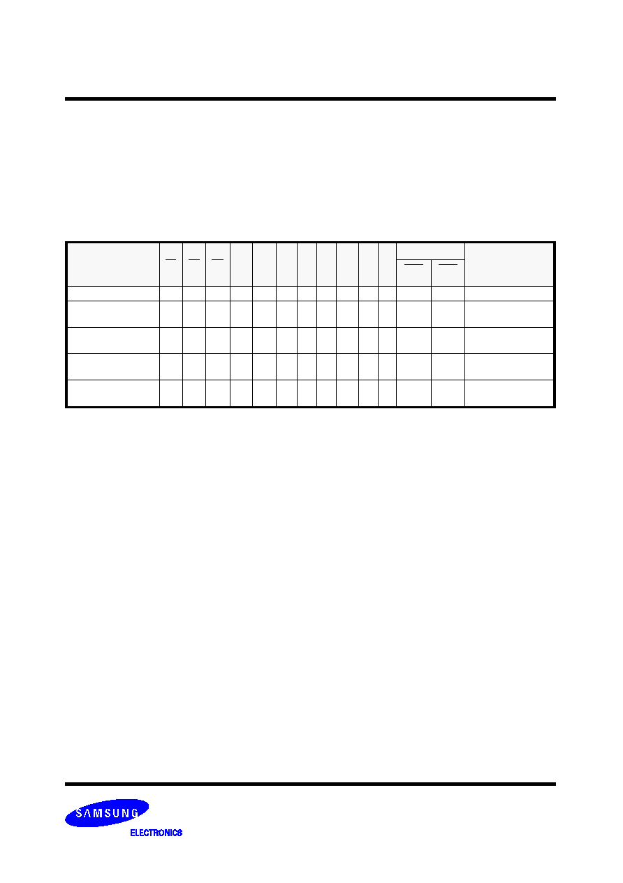
PRODUCT INTRODUCTION
The K8D6316U is an 64Mbit (67,108,864 bits) NOR-type Flash memory. The device features single voltage power supply operating
within the range of 2.7V to 3.6V. The device is programmed by using the Channel Hot Electron (CHE) injection mechanism which is
used to program EPROMs. The device is erased electrically by using Fowler-Nordheim tunneling mechanism. To provide highly flex-
ible erase and program capability, the device adapts a block memory architecture that divides its memory array into 135 blocks (64-
Kbyte x 127 , 8-Kbyte x 8). Programming is done in units of 8 bits (Byte) or 16 bits (Word). All bits of data in one or multiple blocks
can be erased simultaneously when the device executes the erase operation. To prevent the device from accidental erasing or over-
writing the programmed data, 135 memory blocks can be hardware protected by the block group. Byte/Word modes are available for
read operation. These modes can be selected via BYTE pin. The device provides read access times of 70ns, 80ns and 90ns support-
ing high speed microprocessors to operate without any wait states.
The command set of K8D6316U is fully compatible with standard Flash devices. The device is controlled by chip enable (CE), output
enable (OE) and write enable (WE). Device operations are executed by selective command codes. The command codes to be com-
bined with addresses and data are sequentially written to the command registers using microprocessor write timing.
The command
codes serve as inputs to an internal state machine which controls the program/erase circuitry. Register contents also internally latch
addresses and data necessary to execute the program and erase operations. The K8D6316U is implemented with Internal Program/
Erase Algorithms to execute the program/erase operations. The Internal Program/Erase Algorithms are invoked by program/erase
command sequences. The Internal Program Algorithm automatically programs and verifies data at specified addresses. The Internal
Erase Algorithm automatically pre-programs the memory cell which is not programmed and then executes the erase operation. The
K8D6316U has means to indicate the status of completion of program/erase operations. The status can be indicated via the RY/BY
pin, Data polling of DQ7, or the Toggle bit (DQ6). Once the operations have been completed, the device automatically resets itself to
the read mode. The device requires only 14 mA as active read current and 15 mA for program/erase operations.
Table 7. Operations Table
Operation
CE
OE
WE
BYTE
WP/
ACC
A9
A6
A1
A0
DQ15/
A-1
DQ8/
DQ14
DQ0/
DQ7
RESET
Read
word L
L
H
H
L/H
A9
A6
A1
A0
DQ15
D
OUT
D
OUT
H
byte
L
L
H
L
A9
A6
A1
A0
A-1
High-Z
D
OUT
H
Stand-by
Vcc
±
0.3V
X
X
X
(2)
X
X
X
X
High-Z
High-Z
High-Z
(2)
Output Disable
L
H
H
X
L/H
X
X
X
X
High-Z
High-Z
High-Z
H
Reset
X
X
X
X
L/H
X
X
X
X
High-Z
High-Z
High-Z
L
Write
word
L
H
L
H
(4)
A9
A6
A1
A0
D
IN
D
IN
D
IN
H
byte
L
H
L
L
A9
A6
A1
A0
A-1
High-Z
D
IN
H
Enable Block Group
Protect (3)
L
H
L
X
L/H
X
L
H
L
X
X
D
IN
V
ID
Enable Block Group
Unprotect (3)
L
H
L
X
(4)
X
H
H
L
X
X
D
IN
V
ID
Temporary Block
Group
X
X
X
X
(4)
X
X
X
X
X
X
X
V
ID
Auto Select
Manufacturer ID (5)
L
L
H
X
L/H
V
ID
L
L
L
X
X
Code
(See
Table 9)
H
Auto Select
Device Code (5)
L
L
H
X
L/H
V
ID
L
L
H
X
X
Code
(See
Table 9)
H
Notes :
1. L = V
IL
(Low), H = V
IH
(High), V
ID
= 8.5V~12.5V, D
IN
= Data in, D
OUT
= Data out, X = Don't care.
2. WP/ACC and RESET pin are asserted at Vcc
±
0.3 V or Vss
±
0.3 V in the Stand-by mode.
3. Addresses must be composed of the Block address (A12 - A21).
The Block Protect and Unprotect operations may be implemented via programming equipment too.
Refer to the "Block Group Protection and Unprotection".
4. If WP/ACC
=
V
IL,
the two outermost boot blocks is protected. If WP/ACC
=
V
IH,
the two outermost boot block protection depends on whether those
blocks were last protected or unprotected using the method described in "Block Group Protection and Unprotection". If WP/ACC
=
V
HH
, all blocks
will be temporarily unprotected.
5. Manufacturer and device codes may also be accessed via a command register write sequence. Refer to Table 9.
FLASH MEMORY
K8D6x16UTM / K8D6x16UBM
Revision 1.5
March 2005
14
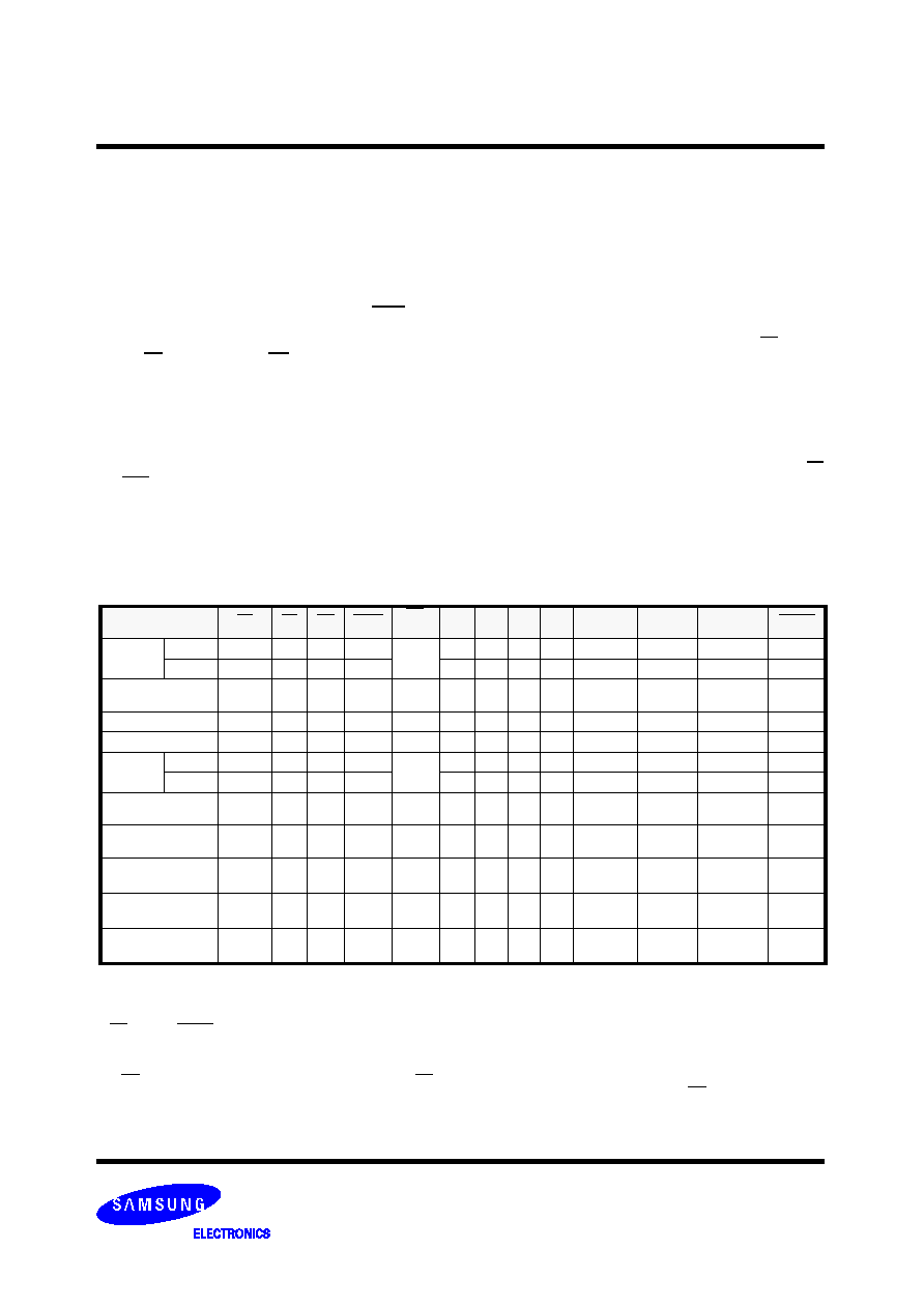
COMMAND DEFINITIONS
The K8D6316U operates by selecting and executing its operational modes. Each operational mode has its own command set. In
order to select a certain mode, a proper command with specific address and data sequences must be written into the command reg-
ister. Writing incorrect information which include address and data or writing an improper command will reset the device to the read
mode. The defined valid register command sequences are stated in Table 8. Note that Erase Suspend (B0H) and Erase Resume
(30H) commands are valid only while the Block Erase Operation is in progress.
Table 8. Command Sequences
Command Sequence
Cycle
1st Cycle
2nd Cycle
3rd Cycle
4th Cycle
5th Cycle
6th Cycle
Word
Byte
Word
Byte
Word
Byte
Word
Byte
Word
Byte
Word
Byte
Read
Addr
1
RA
Data
RD
Reset
Addr
1
XXXH
Data
F0H
Autoselect
Manufacturer
ID (2,3)
Addr
4
555H
AAAH
2AAH
555H
DA/
555H
DA/
AAAH
DA/
X00H
DA/
X00H
Data
AAH 55H
90H
ECH
Autoselect
Device Code
(2,3)
Addr
4
555H
AAAH
2AAH
555H
DA/
555H
DA/
AAAH
DA/
X01H
DA/
X02H
Data
AAH 55H
90H
(See
Table
9)
Autoselect
Block Group
Protect Verify
(2,3)
Addr
4
555H
AAAH
2AAH
555H
DA/
555H
DA/
AAAH
BA /
X02H
BA/
X04H
Data
AAH 55H
90H
(See Table 9)
Auto Select
Secode Block
Factory Protect
Verify (2,3)
Addr
4
555H
AAAH
2AAH
555H
DA/
555H
DA/
AAAH
DA /
X03H
DA/
X06H
Data
AAH 55H
90H
(See Table 9)
Enter Secode
Block Region
Addr
3
555H
AAAH
2AAH
555H
555H
AAAH
Data
AAH 55H
88H
Exit Secode
Block Region
Addr
4
555H
AAAH
2AAH
555H
555H
AAAH XXXH
Data
AAH 55H
90H
00H
Program
Addr
4
555H
AAAH
2AAH
555H
555H
AAAH PA
Data
AAH
55H
A0H
PD
Unlock Bypass
Addr
3
555H
AAAH
2AAH
555H
555H
AAAH
Data
AAH
55H
20H
Unlock Bypass
Program
Addr
2
XXXH
PA
Data
A0H
PD
Unlock Bypass
Reset
Addr
2
XXXH
XXXH
Data
90H
00H
Chip Erase
Addr
6
555H
AAAH
2AAH
555H
555H
AAAH 555H
AAAH
2AAH
555H
555H
AAAH
Data
AAH
55H
80H
AAH
55H
10H
Block Erase
Addr
6
555H
AAAH
2AAH
555H
555H
AAAH 555H
AAAH
2AAH
555H
BA
Data
AAH
55H
80H
AAH
55H
30H
Block Erase
Suspend (4, 5)
Addr
1
XXXH
Data
B0H
Block Erase
Resume
Addr
1
XXXH
Data
30H
CFI Query (6)
Addr
1
55H
AAH
Data
98H
FLASH MEMORY
K8D6x16UTM / K8D6x16UBM
Revision 1.5
March 2005
15
Notes : 1. RA : Read Address, PA : Program Address, RD : Read Data, PD : Program Data
DA : Dual Bank Address (A20 - A21), BA : Block Address (A12 - A21), X = Don't care .
2. To terminate the Autoselect Mode, it is necessary to write Reset command to the register.
3. The 4th cycle data of Autoselect mode is output data.
The 3rd and 4th cycle bank addresses of Autoselect mode must be same.
4. The Read / Program operations at non-erasing blocks and the autoselect mode are allowed in the Erase Suspend mode.
5. The Erase Suspend command is applicable only to the Block Erase operation.
6. Command is valid when the device is in read mode or Autoselect mode.
7. DQ8 - DQ15 are don't care in command sequence, but RD and PD is excluded.
8. A11 - A21 are also don't care, except for the case of special notice.
Description
CE
OE
WE
A21
to
A12
A11
to
A10
A9
A8
to
A7
A6
A5
to
A2
A1
A0
DQ8 to DQ15
DQ7
to
DQ0
BYTE
=V
IH
BYTE
=V
IL
Manufacturer ID
L
L
H
DA
X
V
ID
X
L
X
L
L
X
X
ECH
Device Code K8D6316UT
(Top Boot Block)
L
L
H
DA
X
V
ID
X
L
X
L
H
22H
X
E0H
Device Code K8D6316UB
(Bottom Boot Block)
L
L
H
DA
X
V
ID
X
L
X
L
H
22H
X
E2H
Block Protection
Verification
L
L
H
BA
X
V
ID
X
L
X
H
L
X
X
01H (Protected),
00H (Unprotected)
Secode
Block (2)
Indicator Bit (DQ7)
L
L
H
DA
X
V
ID
X
L
X
H
H
X
X
80H (Factory locked),
00H (Not factory locked)
Table 9. K8D6316U Autoselect Codes, (High Voltage Method)
Notes : 1. L=Logic Low=V
IL
, H=Logic High=V
IH
, DA=Dual Bank Address, BA=Block Address, X=Don't care.
2. Secode Block : Security Code Block.

FLASH MEMORY
K8D6x16UTM / K8D6x16UBM
Revision 1.5
March 2005
16
DEVICE OPERATION
Byte/Word Mode
If the BYTE pin is set at logical "1" , the device is in word mode, DQ0-DQ15 are active. Otherwise the BYTE pin is set at logical "0" ,
the device is in byte mode, DQ0-DQ7 are active. DQ8-DQ14 are in the High-Z state and DQ15 pin is used as an input for the LSB
(A-1) address pin.
Read Mode
The K8D6316U is controlled by Chip Enable (CE), Output Enable (OE) and Write Enable (WE). When CE and OE are low and WE
is high, the data stored at the specified address location,will be the output of the device. The outputs are in high impedance state
whenever CE or OE is high.
Standby Mode
The K8D6316U features Stand-by Mode to reduce power consumption. This mode puts the device on hold when the device is dese-
lected by making CE high (CE = V
IH
). Refer to the DC characteristics for more details on stand-by modes.
Output Disable
The device outputs are disabled when OE is High (OE = V
IH
). The output pins are in high impedance state.
Automatic Sleep Mode
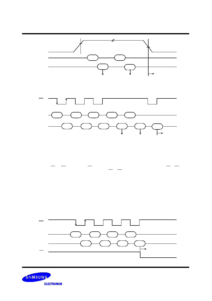
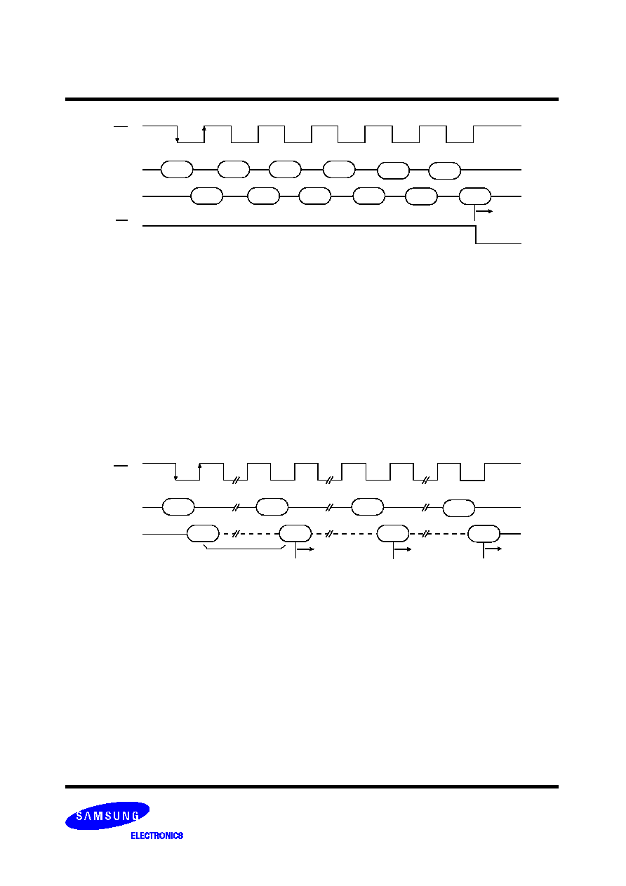
K8D6316U features Automatic Sleep Mode to minimize the device power consumption. Since the device typically draws 10
µ
A of
the current in Automatic Sleep Mode, this feature plays an extremely important role in battery-powered applications. When
addresses remain steady for t
AA
+50ns, the device automatically activates the Automatic Sleep Mode. In the sleep mode, output data
is latched and always available to the system. When addresses are changed, the device provides new data without wait time.
Data
Outputs
t
AA
+ 50ns
Data
Auto Sleep Mode
Address
Data
Data
Data
Data
Figure 1. Auto Sleep Mode Operation
Autoselect Mode
The K8D6316U offers the Autoselect Mode to identify manufacturer and device type by reading a binary code. The Autoselect Mode
allows programming equipment to automatically match the device to be programmed with its corresponding programming algorithm.
In addition, this mode allows the verification of the status of write protected blocks. This mode is used by two method. The one is high
voltage method to be required V
ID
(8.5V~12.5V) on address pin A9. When A9 is held at V
ID
and the bank address or block address is
asserted, the device outputs the valid data via DQ pins(see Table 9 and Figure 2). The rest of addresses except A0, A1 and A6 are
Don
t Care. The other is autoselect command method that the autoselect code is accessible by the commamd sequence without V
ID.
The manufacturer and device code may also be read via the command register. The Command Sequence is shown in Table 8 and
Figure 3. The autoselect operation of block protect verification is initiated by first writing two unlock cycle. The third cycle must con-
tain the bank address and autoselect command (90H). If Block address while (A6, A1, A0) = (0,1,0) is finally asserted on the address
pin, it will produce a logical "1" at the device output DQ0 to indicate a write protected block or a logical "0" at the device output DQ0
to indicate a write unprotected block. To terminate the autoselect operation, write Reset command (F0H) into the command register.
FLASH MEMORY
K8D6x16UTM / K8D6x16UBM
Revision 1.5
March 2005
17
Figure 3. Autoselect Operation ( by command sequence method )
WE
555H/
AAAH
2AAH/
555H
555H/
AAAH
AAH
55H
90H
00H/
01H/
ECH
Manufacturer
Code
Device Code
A21
A0(x16)/*
DQ15
DQ0
F0H
Return to
Read Mode
Write (Program/Erase) Mode
The K8D6316U executes its program/erase operations by writing commands into the command register. In order to write the com-
mands to the register, CE and WE must be low and OE must be high. Addresses are latched on the falling edge of CE or WE (which-
ever occurs last) and the data are latched on the rising edge of CE or WE (whichever occurs first). The device uses standard
microprocessor write timing.
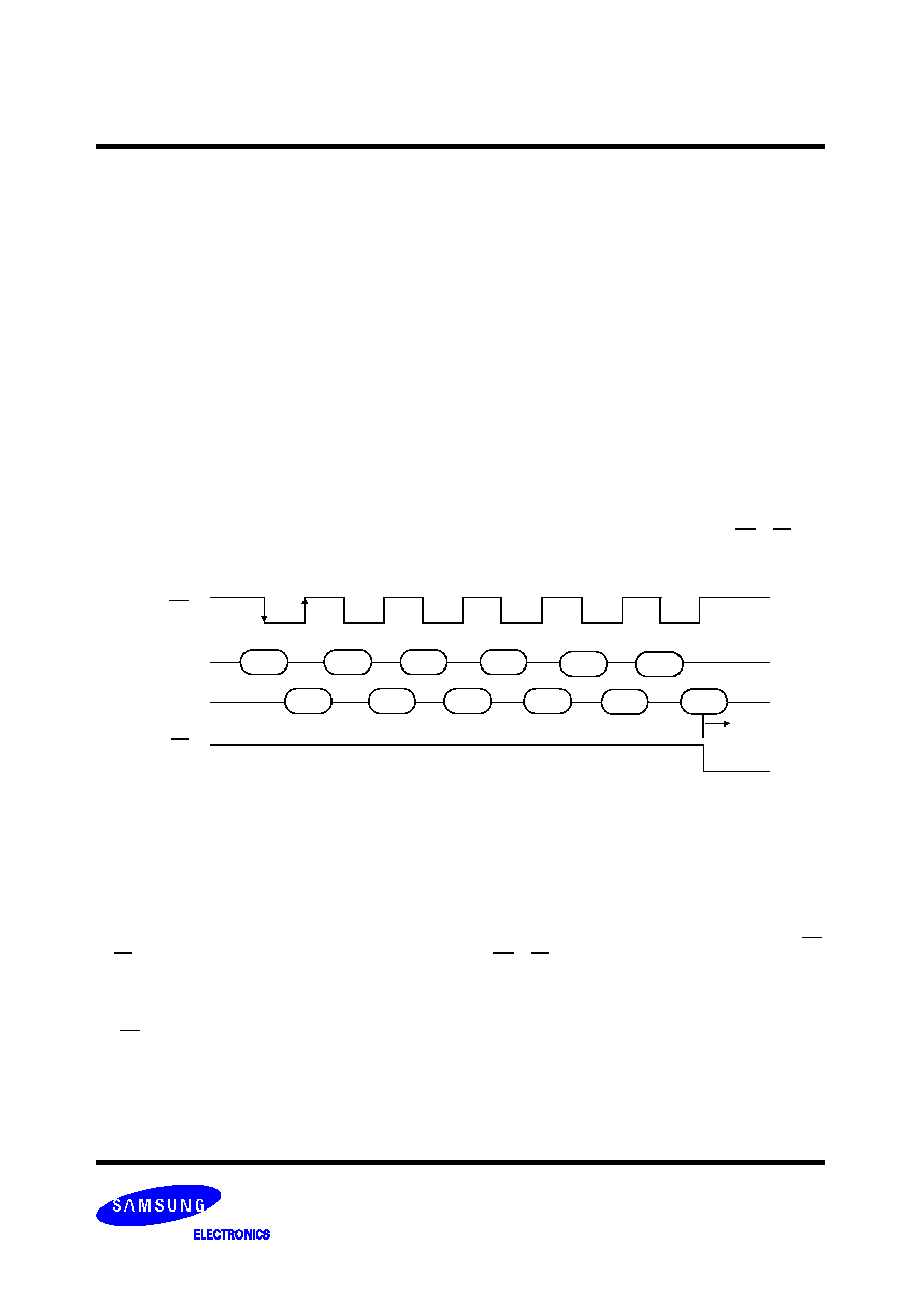
Program
The K8D6316U can be programmed in units of a word or a byte. Programming is writing 0's into the memory array by executing the
Internal Program Routine. In order to perform the Internal Program Routine, a four-cycle command sequence is necessary. The first
two cycles are unlock cycles. The third cycle is assigned for the program setup command. In the last cycle, the address of the mem-
ory location and the data to be programmed at that location are written. The device automatically generates adequate program
pulses and verifies the programmed cell margin by the Internal Program Routine. During the execution of the Routine, the system is
not required to provide further controls or timings.
During the Internal Program Routine, commands written to the device will be ignored. Note that a hardware reset during a program
operation will cause data corruption at the corresponding location.
Figure 4. Program Command Sequence
WE
555H/
AAAH
2AAH/
555H
555H/
AAAH
AAH
55H
A0H
Program
Program
Program
Start
DQ15-DQ0
Address
Data
RY/BY
A9
V
ID
00H
01H
ECH
22E0H
or
22E2H
Manufacturer
Code
Device Code
A6,A1,A0*
DQ15-DQ0
Figure 2. Autoselect Operation ( by high voltage method )
Return to
Read Mode
V = V
IH
or V
IL
22E0H
or
22E2H
Note : The addresses other than A0 , A1 and A6 are Don
t care. Please refer to Table 9 for device code.
Note : The 3rd Cycle and 4th Cycle address must include the same bank address. Please refer to Table 9 for device code.
(
K8D6316U
)
(K8D6316U)
A21
A-1(x8)
A21
A0(x16)/
A21
A-1(x8)
00H
02H
FLASH MEMORY
K8D6x16UTM / K8D6x16UBM
Revision 1.5
March 2005
18
Unlock Bypass
The K8D6316U provides the unlock bypass mode to save its program time for program operation. The mode is invoked by the unlock
bypass command sequence. Then, the unlock bypass program command sequence is required to program the device.
Unlike the standard program command sequence that contains four bus cycles, the unlock bypass program command sequence
comprises only two bus cycles.
The unlock bypass mode is engaged by issuing the unlock bypass command sequence which is comprised of three bus cycles. Writ-
ing first two unlock cycles is followed by a third cycle containing the unlock bypass command (20H). Once the device is in the unlock
bypass mode, the unlock bypass program command sequence is necessary to program in this mode. The unlock bypass program
command sequence is comprised of only two bus cycles; writing the unlock bypass program command
(A0H) is followed by the pro-
gram address and data. This command sequence is the only valid one for programming the device in the unlock bypass mode.
The unlock bypass reset command sequence is the only valid command sequence to exit the unlock bypass mode. The unlock
bypass reset command sequence consists of two bus cycles. The first cycle must contain the data (90H). The second cycle contains
only the data (00H). Then, the device returns to the read mode.
Chip Erase
To erase a chip is to write 1
s into the entire memory array by executing the Internal Erase Routine. The Chip Erase requires six bus
cycles to write the command sequence. The erase set-up command is written after first two "unlock" cycles. Then, there are two
more write cycles prior to writing the chip erase command. The Internal Erase Routine automatically pre-programs and verifies the
entire memory for an all zero data pattern prior to erasing. The automatic erase begins on the rising edge of the last WE or CE pulse
in the command sequence and terminates when DQ7 is "1". After that the device returns to the read mode.
Figure 5. Chip Erase Command Sequence
WE
555H/
AAAH
2AAH/
555H
555H/
AAAH
AAH
55H
80H
555H
Chip Erase
Start
DQ15-DQ0
AAAH
2AAH/
555H
AAH
55H
10H
RY/BY
555H/
AAAH
A21
A0(x16)/
A21
A-1(x8)
Block Erase
To erase a block is to write 1
s into the desired memory block by executing the Internal Erase Routine. The Block Erase requires six
bus cycles to write the command sequence shown in Table 8. After the first two "unlock" cycles, the erase setup command (80H) is
written at the third cycle. Then there are two more "unlock" cycles followed by the Block Erase command. The Internal Erase Routine
automatically pre-programs and verifies the entire memory prior to erasing it. The block address is latched on the falling edge of WE
or CE, while the Block Erase command is latched on the rising edge of WE or CE.
Multiple blocks can be erased sequentially by writing the six bus-cycle operation in Figure 6. Upon completion of the last cycle for the
Block Erase, additional block address and the Block Erase command (30H) can be written to perform the Multi-Block Erase. An 50
µ
s
(typical) "time window" is required between the Block Erase command writes. The Block Erase command must be written within the
50
µ
s "time window", otherwise the Block Erase command will be ignored. The 50
µ
s "time window" is reset when the falling edge of
the WE occurs within the 50
µ
s of "time window" to latch the Block Erase command. During the 50
µ
s of "time window", any command
other than the Block Erase or the Erase Suspend command written to the device will reset the device to read mode. After the 50
µ
s of
"time window", the Block Erase command will initiate the Internal Erase Routine to erase the selected blocks. Any Block Erase
address and command following the exceeded "time window" may or may not be accepted. No other commands will be recognized
except the Erase Suspend command during Block Erase operation.
FLASH MEMORY
K8D6x16UTM / K8D6x16UBM
Revision 1.5
March 2005
19
WE
555H/
AAAH
2AAH/
555H
555H/
AAAH
AAH
55H
80H
555H/
Block Erase
Start
DQ15-DQ0
AAAH
2AAH/
555H
Block
Address
AAH
55H
30H
RY/BY
WE
DQ15-DQ0
Figure 7. Erase Suspend/Resume Command Sequence
Erase Suspend / Resume
The Erase Suspend command interrupts the Block Erase to read or program data in a block that is not being erased. The Erase Sus-
pend command is only valid during the Block Erase operation including the time window of 50
µ
s. The Erase Suspend command is
not valid while the Chip Erase
or the Internal Program Routine sequence is running.
When the Erase Suspend command is written during a Block Erase operation, the device requires a maximum of 20
µ
s to suspend
the erase operation. But, when the Erase Suspend command is written during the block erase time window (50
µ
s) , the device imme-
diately terminates the block erase time window and suspends the erase operation.
After the erase operation has been suspended, the device is availble for reading or programming data in a block that is not being
erased. The system may also write the autoselect command sequence when the device is in the Erase Suspend mode.
When the Erase Resume command is executed, the Block Erase operation will resume. When the Erase Suspend or Erase Resume
command is executed, the addresses are in Don't Care state.
Figure 6. Block Erase Command Sequence
A21
A0(x16)/
A21
A-1(x8)
A21
A0(x16)/
A21
A-1(x8)
555H/
AAAH
Block
Address
AAH
30H
XXXH
Erase
Resume
XXXH
B0H
30H
Erase
Suspend
Block Erase
Start
Block Erase
Command Sequence
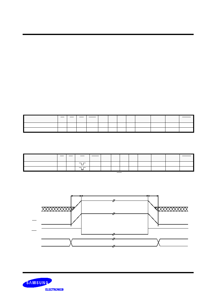
FLASH MEMORY
K8D6x16UTM / K8D6x16UBM
Revision 1.5
March 2005
20
Read While Write
The K8D6316U provides dual bank memory architecture that divides the memory array into two banks. The device is capable of
reading data from one bank and writing data to the other bank simultaneously. This is so called the Read While Write operation with
dual bank architecture; this feature provides the capability of executing the read operation during Program/Erase or Erase-Suspend-
Program operation.
The Read While Write operation is prohibited during the chip erase operation. It is also allowed during erase operation when either
single block or multiple blocks from same bank are loaded to be erased. It means that the Read While Write operation is prohibited
when blocks from Bank1 and another blocks from Bank2 are loaded all together for the multi-block erase operation.
Block Group Protection & Unprotection
The K8D6316U feature hardware block group protection. This feature will disable both program and erase operations in any combi-
nation of forty one block groups of memory. Please refer to Tables 10 and 11. The block group protection feature is enabled using
programming equipment at the user's site. The device is shipped with all block groups unprotected.
This feature can be hardware protected or unprotected. If a block is protected, program or erase command in the protected block will
be ignored by the device. The protected block can only be read. This is useful method to preserve an important program data. The
block group unprotection allows the protected blocks to be erased or programed. All blocks must be protected before unprotect oper-
ation is executing. The block group protection and unprotection can be implemented by two methods.
The first method needs the following conditions.
Operation
CE
OE
WE
BYTE
A9
A6
A1
A0
DQ15/
A-1
DQ8/
DQ14
DQ0/
DQ7
RESET
Block Group Protect
L
H
L
X
X
L
H
L
X
X
D
IN
V
ID
Block Group Unprotect
L
H
L
X
X
H
H
L
X
X
D
IN
V
ID
The K8D6316U needs the recovery time (20
µ
s) from the rising edge of WE in order to execute its program, erase and read opera-
tions.
Operation
CE
OE
WE
BYTE
A9
A6
A1
A0
DQ15/
A-1
DQ8/
DQ14
DQ0/
DQ7
RESET
Block Group Protect
L
V
ID
X
V
ID
L
H
L
X
X
X
H
Block Group Unprotect
L
V
ID
X
V
ID
H
H
L
X
X
X
H
A9
OE
Don
'
t Care
WE
Address
Don
'
t Care
500ns
500ns
Block Group Address*
Figure 8. Block Group Protect Sequence (The second method)
Block Group Protect:150
µ
s
Block Group Unprotect:500ms
Notes : * Block Group Address is Don't Care during Block Group Unprotection.
Address must be inputted to the block group address (A12~A21) during block group protection operation. Please refer to Figure 9
(Algorithm) and Switching Waveforms of Block Group Protect & Unprotect Operations.
The second method needs the following conditions in order to keep backward compatibility. Please refer to Figure 8.
Low
V
ID
V
ID
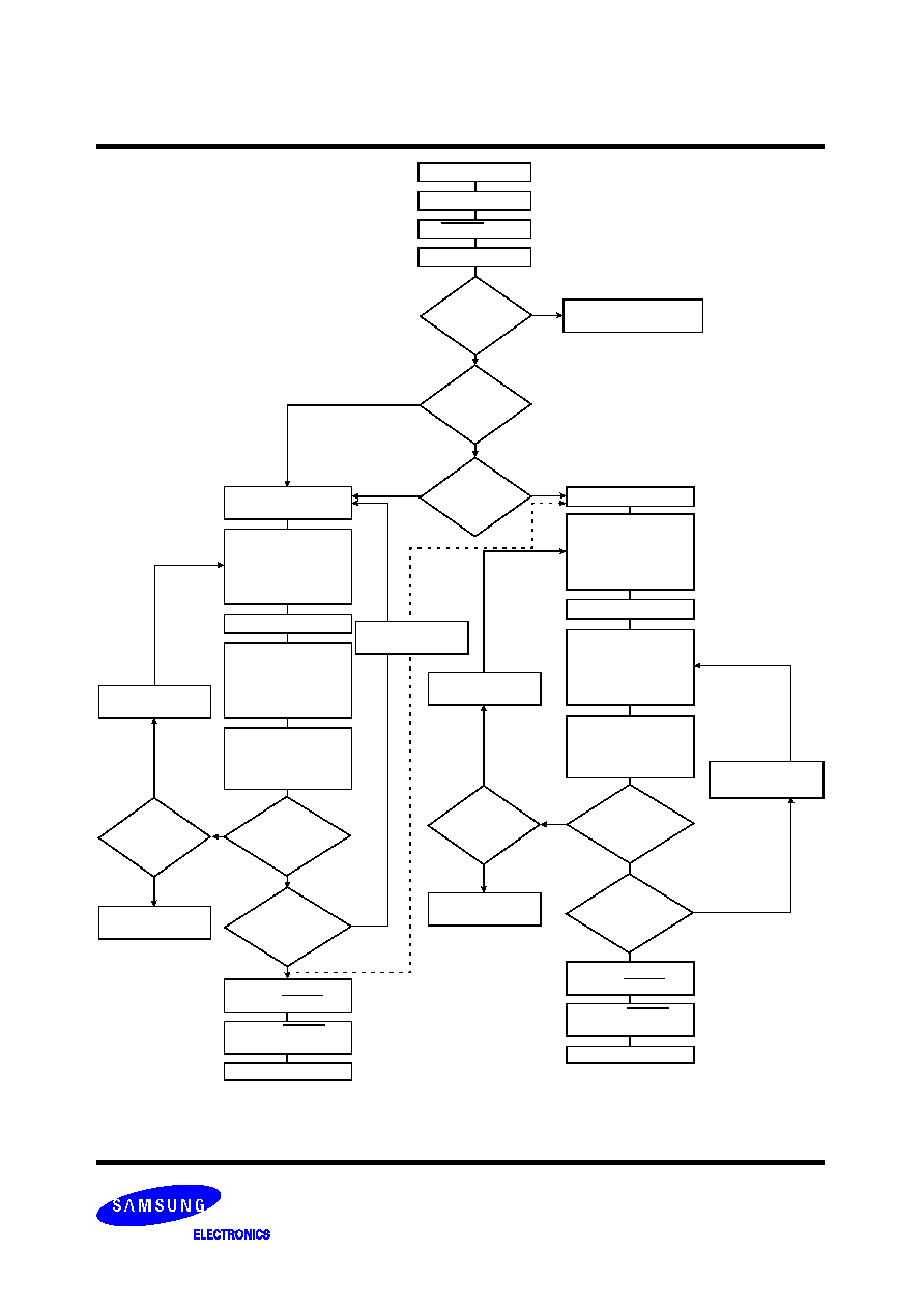
FLASH MEMORY
K8D6x16UTM / K8D6x16UBM
Revision 1.5
March 2005
21
Figure 9. Block Group Protection & Unprotection Algorithms
Block Protect
Algorithm
Set up Block Group
address
Block Group Protect:
Write 60H to Block
Group address with
A6=0,A1=1
A0=0
Wait 150
µ
s
Verify Block Group
Protect:Write 40H to
Block Group address
with A6=0,
A1=1,A0=0
Read from
Block Group address
with A6=0,
A1=1,A0=0
Data=01h?
Protect another
Block Group?
Remove V
ID
from RESET
Write RESET
command
END
Wait 1
µ
s
First Write
Cycle=60h?
Temporary Block Group
Unprotect Mode
Block Group Unprotect
Write 60H
with
A6=1,A1=1
A0=0
Wait 15ms
Verify Block Group
Unprotect:Write 40H to
Block Group address
with A6=1,
A1=1,A0=0
Read from
Block Group address
with A6=1,
A1=1,A0=0
Data=00h?
Last Block Group
Remove VID
from RESET
Write RESET
command
END
No
Increment
COUNT
COUNT
=1000?
Device failed
No
Yes
Yes
No
No
Yes
Algorithm
Increment
COUNT
COUNT
=25?
Device failed
No
Yes
No
All Block Groups
Protected ?
No
Block Group <i>, i= 0
START
COUNT = 1
RESET=V
ID
Yes
Yes
Yes
No
Note : All blocks must be protected before unprotect operation is executing.
verified ?
Block Group
Protection ?
Yes
No
Yes
Set up next Block
Reset
COUNT=1
Block Unprotect
Group address
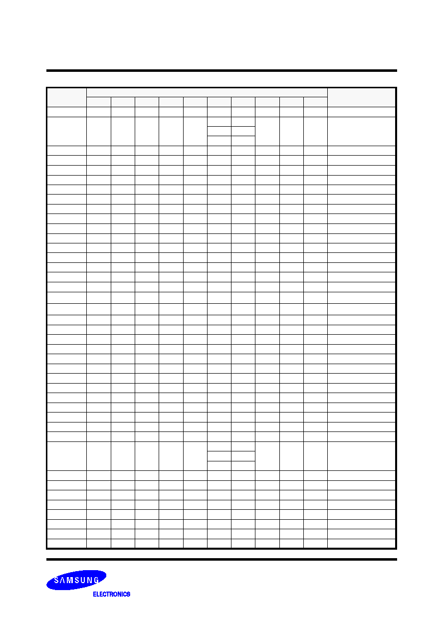
FLASH MEMORY
K8D6x16UTM / K8D6x16UBM
Revision 1.5
March 2005
22
Table 10. Block Group Address (Top Boot Block)
Block Group
Block Address
Block
A21
A20
A19
A18
A17
A16
A15
A14
A13
A12
BGA0
0
0
0
0
0
0
0
X
X
X
BA0
BGA1
0
0
0
0
0
0
1
X
X
X
BA1 to BA3
1
0
1
1
BGA2
0
0
0
0
1
X
X
X
X
X
BA4 to BA7
BGA3
0
0
0
1
0
X
X
X
X
X
BA8 to BA11
BGA4
0
0
0
1
1
X
X
X
X
X
BA12 to BA15
BGA5
0
0
1
0
0
X
X
X
X
X
BA16 to BA19
BGA6
0
0
1
0
1
X
X
X
X
X
BA20 to BA23
BGA7
0
0
1
1
0
X
X
X
X
X
BA24 to BA27
BGA8
0
0
1
1
1
X
X
X
X
X
BA28 to BA31
BGA9
0
1
0
0
0
X
X
X
X
X
BA32 to BA35
BGA10
0
1
0
0
1
X
X
X
X
X
BA36 to BA39
BGA11
0
1
0
1
0
X
X
X
X
X
BA40 to BA43
BGA12
0
1
0
1
1
X
X
X
X
X
BA44 to BA47
BGA13
0
1
1
0
0
X
X
X
X
X
BA48 to BA51
BGA14
0
1
1
0
1
X
X
X
X
X
BA52 to BA55
BGA15
0
1
1
1
0
X
X
X
X
X
BA56 to BA59
BGA16
0
1
1
1
1
X
X
X
X
X
BA60 to BA63
BGA17
1
0
0
0
0
X
X
X
X
X
BA64 to BA67
BGA18
1
0
0
0
1
X
X
X
X
X
BA68 to BA71
BGA19
1
0
0
1
0
X
X
X
X
X
BA72 to BA75
BGA20
1
0
0
1
1
X
X
X
X
X
BA76 to BA79
BGA21
1
0
1
0
0
X
X
X
X
X
BA80 to BA83
BGA22
1
0
1
0
1
X
X
X
X
X
BA84 to BA87
BGA23
1
0
1
1
0
X
X
X
X
X
BA88 to BA91
BGA24
1
0
1
1
1
X
X
X
X
X
BA92 to BA95
BGA25
1
1
0
0
0
X
X
X
X
X
BA96 to BA99
BGA26
1
1
0
0
1
X
X
X
X
X
BA100 to BA103
BGA27
1
1
0
1
0
X
X
X
X
X
BA104 to BA107
BGA28
1
1
0
1
1
X
X
X
X
X
BA108 to BA111
BGA29
1
1
1
0
0
X
X
X
X
X
BA112 to BA115
BGA30
1
1
1
0
1
X
X
X
X
X
BA116 to BA119
BGA31
1
1
1
1
0
X
X
X
X
X
BA120 to BA123
BGA32
1
1
1
1
1
0
0
X
X
X
BA124 to BA126
0
1
1
0
BGA33
1
1
1
1
1
1
1
0
0
0
BA127
BGA34
1
1
1
1
1
1
1
0
0
1
BA128
BGA35
1
1
1
1
1
1
1
0
1
0
BA129
BGA36
1
1
1
1
1
1
1
0
1
1
BA130
BGA37
1
1
1
1
1
1
1
1
0
0
BA131
BGA38
1
1
1
1
1
1
1
1
0
1
BA132
BGA39
1
1
1
1
1
1
1
1
1
0
BA133
BGA40
1
1
1
1
1
1
1
1
1
1
BA134
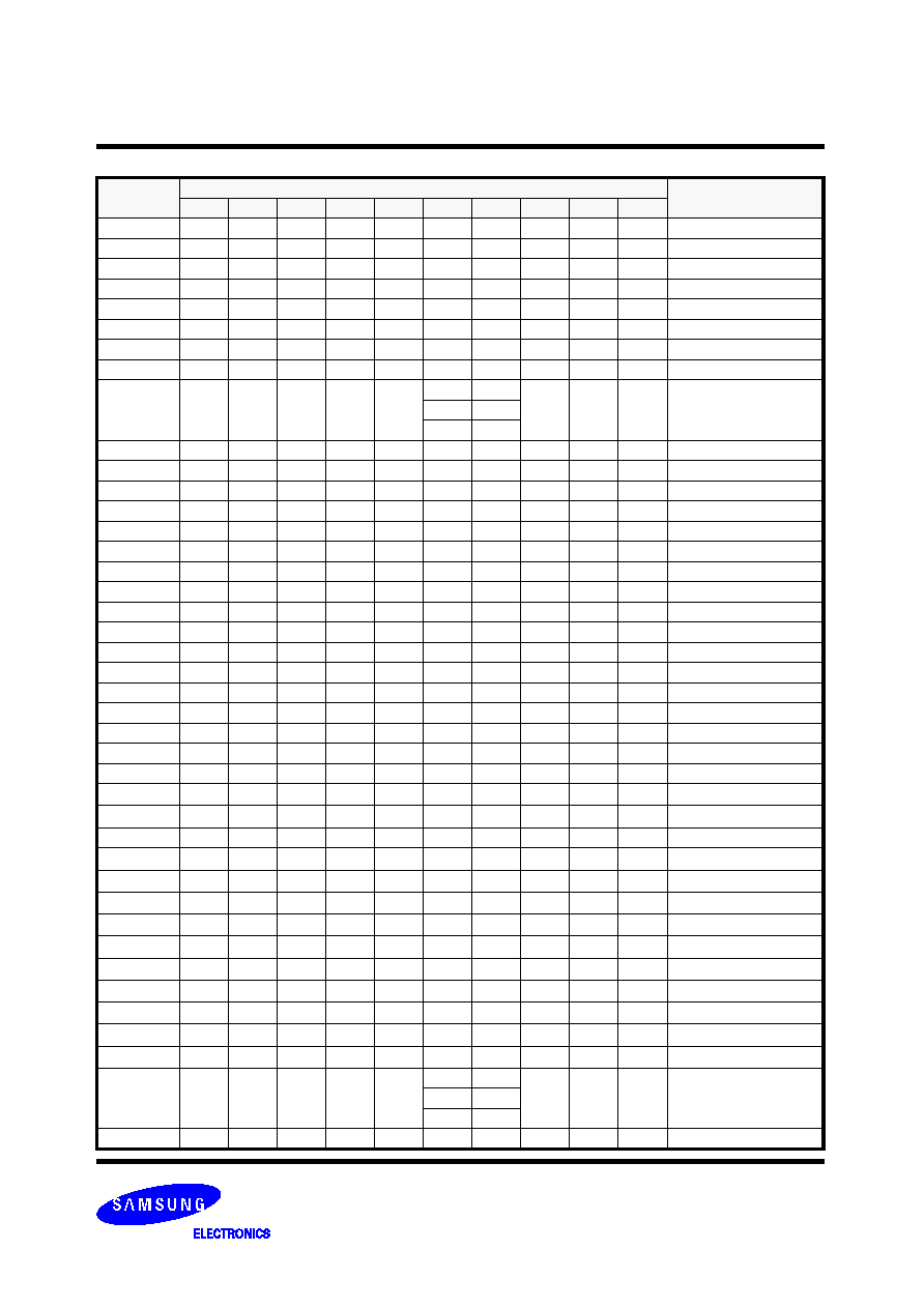
FLASH MEMORY
K8D6x16UTM / K8D6x16UBM
Revision 1.5
March 2005
23
Table 11. Block Group Address (Bottom Boot Block)
Block Group
Block Address
Block
A21
A20
A19
A18
A17
A16
A15
A14
A13
A12
BGA0
0
0
0
0
0
0
0
0
0
0
BA0
BGA1
0
0
0
0
0
0
0
0
0
1
BA1
BGA2
0
0
0
0
0
0
0
0
1
0
BA2
BGA3
0
0
0
0
0
0
0
0
1
1
BA3
BGA4
0
0
0
0
0
0
0
1
0
0
BA4
BGA5
0
0
0
0
0
0
0
1
0
1
BA5
BGA6
0
0
0
0
0
0
0
1
1
0
BA6
BGA7
0
0
0
0
0
0
0
1
1
1
BA7
BGA8
0
0
0
0
0
0
1
X
X
X
BA8 to BA10
1
0
1
1
BGA9
0
0
0
0
1
X
X
X
X
X
BA11 to BA14
BGA10
0
0
0
1
0
X
X
X
X
X
BA15 to BA18
BGA11
0
0
0
1
1
X
X
X
X
X
BA19 to BA22
BGA12
0
0
1
0
0
X
X
X
X
X
BA23 to BA26
BGA13
0
0
1
0
1
X
X
X
X
X
BA27 to BA30
BGA14
0
0
1
1
0
X
X
X
X
X
BA31 to BA34
BGA15
0
0
1
1
1
X
X
X
X
X
BA35 to BA38
BGA16
0
1
0
0
0
X
X
X
X
X
BA39 to BA42
BGA17
0
1
0
0
1
X
X
X
X
X
BA43 to BA46
BGA18
0
1
0
1
0
X
X
X
X
X
BA47 to BA50
BGA19
0
1
0
1
1
X
X
X
X
X
BA51 to BA54
BGA20
0
1
1
0
0
X
X
X
X
X
BA55 to BA58
BGA21
0
1
1
0
1
X
X
X
X
X
BA59 to BA62
BGA22
0
1
1
1
0
X
X
X
X
X
BA63 to BA66
BGA23
0
1
1
1
1
X
X
X
X
X
BA67 to BA70
BGA24
1
0
0
0
0
X
X
X
X
X
BA71 to BA74
BGA25
1
0
0
0
1
X
X
X
X
X
BA75 to BA78
BGA26
1
0
0
1
0
X
X
X
X
X
BA79 to BA82
BGA27
1
0
0
1
1
X
X
X
X
X
BA83 to BA86
BGA28
1
0
1
0
0
X
X
X
X
X
BA87to BA90
BGA29
1
0
1
0
1
X
X
X
X
X
BA91 to BA94
BGA30
1
0
1
1
0
X
X
X
X
X
BA95 to BA98
BGA31
1
0
1
1
1
X
X
X
X
X
BA99 to BA102
BGA32
1
1
0
0
0
X
X
X
X
X
BA103 to BA106
BGA33
1
1
0
0
1
X
X
X
X
X
BA107 to BA110
BGA34
1
1
0
1
0
X
X
X
X
X
BA111 to BA114
BGA35
1
1
0
1
1
X
X
X
X
X
BA115 to BA118
BGA36
1
1
1
0
0
X
X
X
X
X
BA119 to BA122
BGA37
1
1
1
0
1
X
X
X
X
X
BA123 to BA126
BGA38
1
1
1
1
0
X
X
X
X
X
BA127 to BA130
BGA39
1
1
1
1
1
0
0
X
X
X
BA131 to BA133
0
1
1
0
BGA40
1
1
1
1
1
1
1
X
X
X
BA134

FLASH MEMORY
K8D6x16UTM / K8D6x16UBM
Revision 1.5
March 2005
24
Write Protect (WP)
The WP/ACC pin has two useful functions. The one is that certain boot block is protected by the hardware method not to use V
ID
.
The other is that program operation is accelerated to reduce the program time (Refer to Accelerated program Operation Paragraph).
When the WP/ACC pin is asserted at V
IL
, the device can not perform program and erase operation in the two "outermost" 8K byte
boot blocks independently of whether those blocks were protected or unprotected using the method described in "Block Group pro-
tection/Unprotection".
The write protected blocks can only be read. This is useful method to preserve an important program data.
The two outermost 8K byte boot blocks are the two blocks containing the lowest addresses in a bottom-boot-configured device, or
the two blocks containing the highest addresses in a top-boot-congfigured device.
(K8D6316UT : BA133 and BA134, K8D6316UB : BA0 and BA1)
When the WP/ACC pin is asserted at V
IH
, the device reverts to whether the two outermost 8K byte boot blocks were last set to be
protected or unprotected. That is, block protection or unprotection for these two blocks depends on whether they were last protected
or unprotected using the method described in "Block Group protection/unprotection".
Recommend that the WP/ACC pin must not be in the state of floating or unconnected, or the device may be led to malfunction.
Temporary Block Group Unprotect
The protected blocks of the K8D6316U can be temporarily unprotected by applying high voltage (V
ID
= 8.5V~12.5V) to the RESET
pin. In this mode, previously protected blocks can be programmed or erased with the program or erase command routines. When the
RESET pin goes high (RESET = V
IH
), all the previously protected blocks will be protected again. If the WP/ACC pin is asserted at V
IL
, the two outermost boot blocks remain protected.
RESET
Program & Erase Operation
V
ID
V = V
IH
or V
IL
at Protected Block
CE
WE
Figure 10. Temporary Block Group Unprotect Sequence
Secode(Security Code) Block Region
The Secode Block feature provides a Flash memory region to be stored unique and permanent identification code, that is, Electronic
Serial Number (ESN), customer code and so on. This is primarily intended for customers who wish to use an Electronic Serial Num-
ber (ESN) in the device with the ESN protected against modification. Once the Secode Block region is protected, any further modifi-
cation of that region is impossible. This ensures the security of the ESN once the product is shipped to the field.
The Secode Block is factory locked or customer lockable. Before the device is shipped, the factory locked Secode Block is written on
the special code and it is protected. The Secode Indicator bit (DQ7) is permanently fixed at "1" and it is not changed. The customer
lockable Secode Block is unprotected, therefore it is programmed and erased. The Secode Indicator bit (DQ7) of it is permanently
fixed at "0" and it is not changed. but Once it is protected, there is no procedure to unprotect and modify the Secode Block.
The Secode Block region is 64K bytes in length and is accessed through a new command sequence (see Table 8). After the system
has written the Enter Secode Block command sequence, the system may read the Secode Block region by using the same
addresses of the boot blocks (8KBx8). The K8D6316UT occupies the address of the byte mode 7F0000H to 7FFFFFH (word mode
3F8000H to 3FFFFFH) and the K8D6316UB type occupies the address of the byte mode 000000H to 00FFFFH (word mode
000000H to 007FFFH). This mode of operation continues until the system issues the Exit Secode Block command sequence, or until
power is removed from the device. On power-up, or following a hardware reset, the device reverts to read mode.

FLASH MEMORY
K8D6x16UTM / K8D6x16UBM
Revision 1.5
March 2005
25
Accelerated Program Operation
Accelerated program operation reduces the program time. This is one of two functions provided by the WP/ACC pin. When the WP/
ACC pin is asserted as V
HH
, the device automatically enters the aforementioned Unlock Bypass mode, temporarily unprotecting any
protected blocks, and reduces the program operation time. The system would use a two-cycle program command sequence as
required by the Unlock Bypass mode. Removing V
HH
from the WP/ACC pin returns the device to normal operation. Recommend
that the WP/ACC pin must not be asserted at V
HH
except accelerated program operation, or the device may be damaged. In
addition, the WP/ACC pin must not be in the state of floating or unconnected, otherwise the device may be led to malfunc-
tion.
Software Reset
The reset command provides that the bank is reseted to read mode or erase-suspend-read mode. The addresses are in Don't Care
state. The reset command is vaild between the sequence cycles in an erase command sequence before erasing begins, or in a pro-
gram command sequence before programming begins. This resets the bank in which was operating to read mode. if the device is be
erasing or programming, the reset command is invalid until the operation is completed. Also, the reset command is valid between the
sequence cycles in an autoselect command sequence. In the autoselect mode, the reset command returns the bank to read mode.
If a bank entered the autoselect mode in the Erase Suspend mode, the reset command returns the bank to erase-suspend-read
mode. If DQ5 is high on erase or program operation, the reset command return the bank to read mode or erase-suspend-read mode
if the bank was in the Erase Suspend state.
Hardware Reset
The K8D6316U offers a reset feature by driving the RESET pin to V
IL
.
The RESET pin must be kept low (V
IL
) for at least 500ns.
When the RESET pin is driven low, any operation in progress will be terminated and the internal state machine will be reset to the
standby mode after 20
µ
s. If a hardware reset occurs during a program operation, the data at that particular location will be lost.
Once the RESET pin is taken high, the device requires 200ns of wake-up time until outputs are valid for read access. Also, note that
all the data output pins are tri-stated for the duration of the RESET pulse.
The RESET pin may be tied to the system reset pin. If a system reset occurs during the Internal Program and Erase Routine, the
device will be automatically reset to the read mode ; this will enable the systems microprocessor to read the boot-up firmware from
the Flash memory.
Power-up Protection
To avoid initiation of a write cycle during Vcc Power-up, RESET low must be asserted during power-up. After RESET goes high, the
device is reset to the read mode.
Low Vcc Write Inhibit
To avoid initiation of a write cycle during Vcc power-up and power-down, a write cycle is locked out for Vcc less than 1.8V. If Vcc <
V
LKO
(Lock-Out Voltage), the command register and all internal program/erase circuits are disabled. Under this condition the device
will reset itself to the read mode. Subsequent writes will be ignored until the Vcc level is greater than V
LKO
. It is the user
s responsi-
bility to ensure that the control pins are logically correct to prevent unintentional writes when Vcc is above 1.8V.
Write Pulse Glitch Protection
Noise pulses of less than 5ns(typical) on CE, OE, or WE will not initiate a write cycle.
Logical Inhibit
Writing is inhibited under any one of the following conditions : OE = V
IL
,
CE = V
IH
or WE = V
IH
.
To initiate a write, CE and WE must
be "0", while OE is "1".
Commom Flash Memory Interface
Common Flash Momory Interface is contrived to increase the compatibility of host system software. It provides the specific informa-
tion of the device, such as memory size, byte/word configuration, and electrical features. Once this information has been obtained,
the system software will know which command sets to use to enable flash writes, block erases, and control the flash component.
When the system writes the CFI command(98H) to address 55H in word mode(or address AAH in byte mode), the device enters the
CFI mode. And then if the system writes the address shown in Table 12, the system can read the CFI data. Query data are always
presented on the lowest-order data outputs(DQ0-7) only. In word(x16) mode, the upper data outputs(DQ8-15) is 00h. To terminate
this operation, the system must write the reset command.
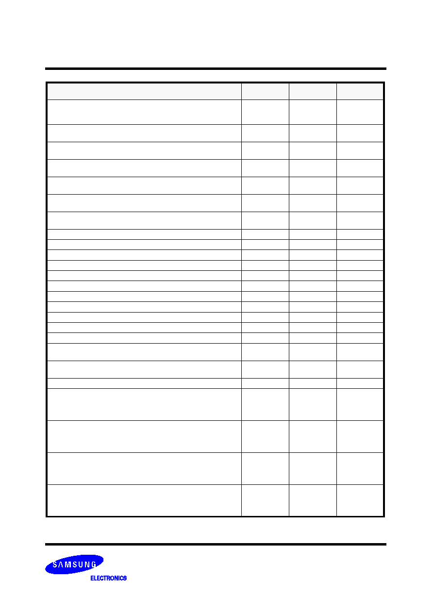
FLASH MEMORY
K8D6x16UTM / K8D6x16UBM
Revision 1.5
March 2005
26
Table 12. Common Flash Memory Interface Code
Description
Addresses
(Word Mode)
Addresses
(Byte Mode)
Data
Query Unique ASCII string "QRY"
10H
11H
12H
20H
22H
24H
0051H
0052H
0059H
Primary OEM Command Set
13H
14H
26H
28H
0002H
0000H
Address for Primary Extended Table
15H
16H
2AH
2CH
0040H
0000H
Alternate OEM Command Set (00h = none exists)
17H
18H
2EH
30H
0000H
0000H
Address for Alternate OEM Extended Table (00h = none exists)
19H
1AH
32H
34H
0000H
0000H
Vcc Min. (write/erase)
D7-D4: volt, D3-D0: 100 millivolt
1BH
36H
0027H
Vcc Max. (write/erase)
D7-D4: volt, D3-D0: 100 millivolt
1CH
38H
0036H
Vpp Min. voltage(00H = no Vpp pin present)
1DH
3AH
0000H
Vpp Max. voltage(00H = no Vpp pin present)
1EH
3CH
0000H
Typical timeout per single byte/word write 2
N
us
1FH
3EH
0004H
Typical timeout for Min. size buffer write 2
N
us(00H = not supported)
20H
40H
0000H
Typical timeout per individual block erase 2
N
ms
21H
42H
000AH
Typical timeout for full chip erase 2
N
ms(00H = not supported)
22H
44H
0000H
Max. timeout for byte/word write 2
N
times typical
23H
46H
0005H
Max. timeout for buffer write 2
N
times typical
24H
48H
0000H
Max. timeout per individual block erase 2
N
times typical
25H
4AH
0004H
Max. timeout for full chip erase 2
N
times typical(00H = not supported)
26H
4CH
0000H
Device Size = 2
N
byte
27H
4EH
0017H
Flash Device Interface description
28H
29H
50H
52H
0002H
0000H
Max. number of byte in multi-byte write = 2
N
2AH
2BH
54H
56H
0000H
0000H
Number of Erase Block Regions within device
2CH
58H
0002H
Erase Block Region 1 Information
2DH
2EH
2FH
30H
5AH
5CH
5EH
60H
0007H
0000H
0020H
0000H
Erase Block Region 2 Information
31H
32H
33H
34H
62H
64H
66H
68H
007EH
0000H
0000H
0001H
Erase Block Region 3 Information
35H
36H
37H
38H
6AH
6CH
6EH
70H
0000H
0000H
0000H
0000H
Erase Block Region 4 Information
39H
3AH
3BH
3CH
72H
74H
76H
78H
0000H
0000H
0000H
0000H

FLASH MEMORY
K8D6x16UTM / K8D6x16UBM
Revision 1.5
March 2005
27
Table 12. Common Flash Memory Interface Code
Note :
1. The number of blocks in Bank2 is device dependent.
K8D6316U(16Mb/48Mb) = 60h (96blocks)
Description
Addresses
(Word Mode)
Addresses
(Byte Mode)
Data
Query-unique ASCII string "PRI"
40H
41H
42H
80H
82H
84H
0050H
0052H
0049H
Major version number, ASCII
43H
86H
0030H
Minor version number, ASCII
44H
88H
0030H
Address Sensitive Unlock(Bits 1-0)
0 = Required, 1= Not Required
Silcon Revision Number(Bits 7-2)
45H
8AH
0000H
Erase Suspend
0 = Not Supported, 1 = To Read Only, 2 = To Read & Write
46H
8CH
0002H
Block Protect
0 = Not Supported, 1 = Supported
47H
8EH
0001H
Block Temporary Unprotect 00 = Not Supported, 01 = Supported
48H
90H
0001H
Block Protect/Unprotect scheme 04 = K8D1x16U mode
49H
92H
0004H
Simultaneous Operation (1)
00 = Not Supported, XX = Number of Blocks in Bank2
4AH
94H
00XXH
Burst Mode Type 00 = Not Supported, 01 = Supported
4BH
96H
0000H
Page Mode Type
00=Not supported, 01=4word page, 02=8word page
4CH
98H
0000H
ACC(Acceleration) Supply Minimum
00 = Not Supported, D7 - D4 : Volt, D3 - D0 : 100mV
4DH
9AH
0085H
ACC(Acceleration) Supply Maximum
00 = Not Supported, D7 - D4 : Volt, D3 - D0 : 100mV
4EH
9CH
00C5H
Top/Bottom Boot Block Flag
02H = Bottom Boot , 03H = Top Boot
4FH
9EH
000XH
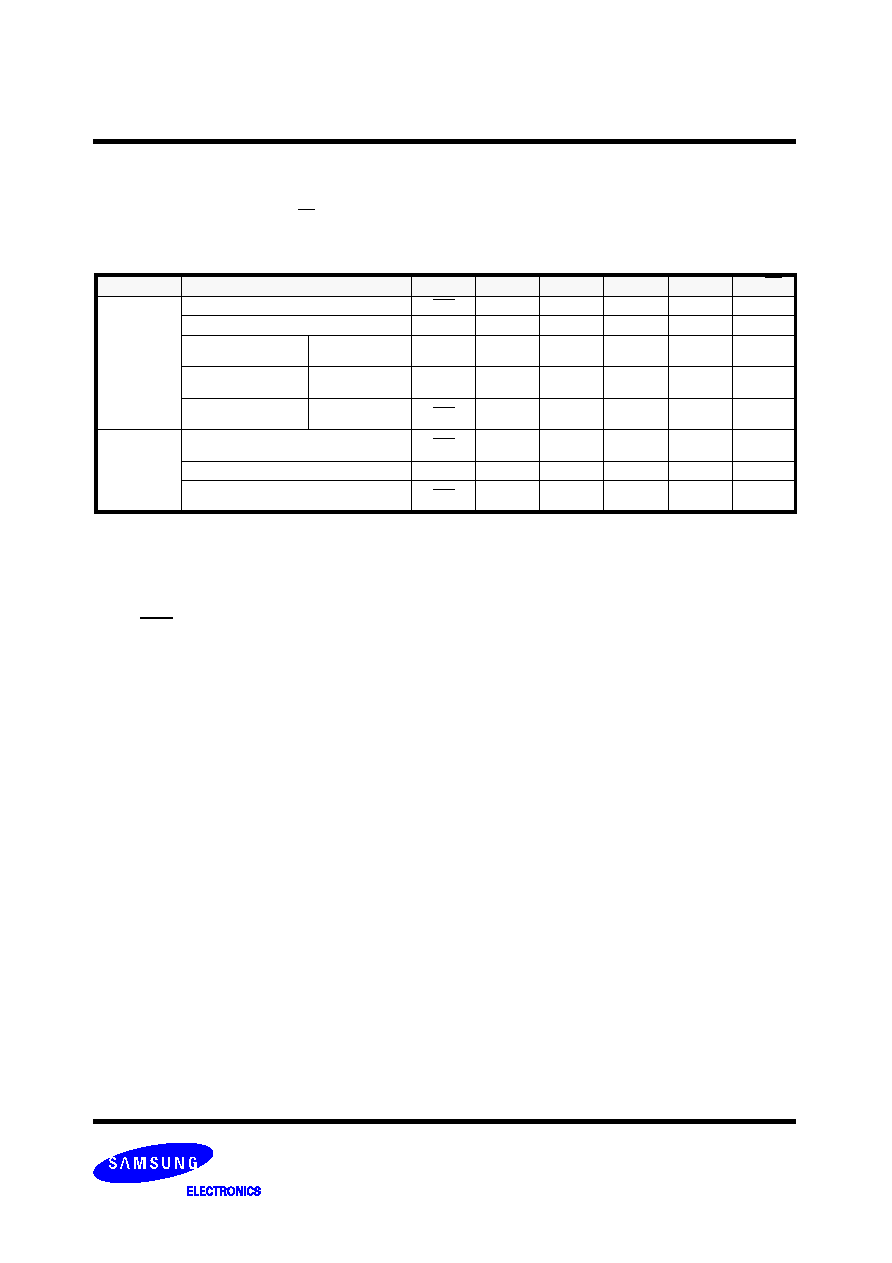
FLASH MEMORY
K8D6x16UTM / K8D6x16UBM
Revision 1.5
March 2005
28
DEVICE STATUS FLAGS
The K8D6316U has means to indicate its status of operation in the bank where a program or erase operation is in processes.
Address must include bank address being excuted internal routine operation. The status is indicated by raising the device status flag
via corresponding DQ pins or the RY/ BY pin. The corresponding DQ pins are DQ7, DQ6, DQ5, DQ3 and DQ2. The statuses are as
follows :
Table 13. Hardware Sequence Flags
Notes :
1. DQ2 will toggle when the device performs successive read operations from the erase suspended block.
2. If DQ5 is High (exceeded timing limits), successive reads from a problem block will cause DQ2 to toggle.
Status
DQ7
DQ6
DQ5
DQ3
DQ2
RY/BY
In Progress
Programming
DQ7
Toggle
0
0
1
0
Block Erase or Chip Erase
0
Toggle
0
1
Toggle
0
Erase Suspend Read
Erase Suspended
Block
1
1
0
0
Toggle
(Note 1)
1
Erase Suspend Read
Non-Erase Sus-
pended Block
Data
Data
Data
Data
Data
1
Erase Suspend
Program
Non-Erase Sus-
pended Block
DQ7
Toggle
0
0
1
0
Exceeded
Time Limits
Programming
DQ7
Toggle
1
0
No
Toggle
0
Block Erase or Chip Erase
0
Toggle
1
1
(Note 2)
0
Erase Suspend Program
DQ7
Toggle
1
0
No
Toggle
0
DQ7 : Data Polling
When an attempt to read the device is made while executing the Internal Program, the complement of the data is written to DQ7 as
an indication of the Routine in progress. When the Routine is completed an attempt to access to the device will produce the true data
written to DQ7. When a user attempts to read the device during the Erase operation, DQ7 will be low. If the device is placed in the
Erase Suspend Mode, the status can be detected via the DQ7 pin. If the system tries to read an address which belongs to a block
that is being erased, DQ7 will be high. If a non-erased block address is read, the device will produce the true data to DQ7. If an
attempt is made to program a protected block, DQ7 outputs complements the data for approximately 1
µ
s and the device then returns
to the Read Mode without changing data in the block. If an attempt is made to erase a protected block, DQ7 outputs complement
data in approximately 100us and the device then returns to the Read Mode without erasing the data in the block.
DQ6 : Toggle Bit
Toggle bit is another option to detect whether an Internal Routine is in progress or completed. Once the device is at a busy state,
DQ6 will toggle. Toggling DQ6 will stop after the device completes its Internal Routine. If the device is in the Erase Suspend Mode,
an attempt to read an address that belongs to a block that is being erased will produce a high output of DQ6. If an address belongs
to a block that is not being erased, toggling is halted and valid data is produced at DQ6.
If an attempt is made to program a protected block, DQ6 toggles for approximately 1us and the device then returns to the Read
Mode without changing the data in the block. If an attempt is made to erase a protected block, DQ6 toggles for approximately 100
µ
s
and the device then returns to the Read Mode without erasing the data in the block.
DQ5 : Exceed Timing Limits
If the Internal Program/Erase Routine extends beyond the timing limits, DQ5 will go High, indicating program/erase failure.
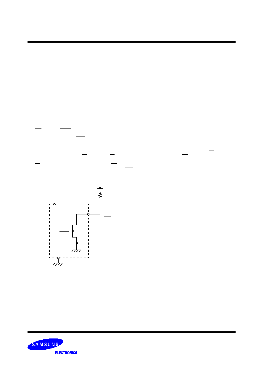
FLASH MEMORY
K8D6x16UTM / K8D6x16UBM
Revision 1.5
March 2005
29
RY/BY : Ready/Busy
The K8D6316U has a Ready / Busy output that indicates either the completion of an operation or the status of Internal Algorithms. If
the output is Low, the device is busy with either a program or an erase operation. If the output is High, the device is ready to accept
any read/write or erase operation. When the RY/ BY pin is low, the device will not accept any additional program or erase commands
with the exception of the Erase Suspend command. If the K8D6316U is placed in an Erase Suspend mode, the RY/ BY output will be
High. For programming, the RY/ BY is valid (RY/ BY = 0) after the rising edge of the fourth WE pulse in the four write pulse
sequence. For Chip Erase, RY/ BY is also valid after the rising edge of WE pulse in the six write pulse sequence. For Block Erase,
RY/ BY is also valid after the rising edge of the sixth WE pulse.
The pin is an open drain output, allowing two or more Ready/ Busy outputs to be OR-tied. An appropriate pull-up resistor is required
for proper operation.
DQ3 : Block Erase Timer
The status of the multi-block erase operation can be detected via the DQ3 pin. DQ3 will go High if 50
µ
s of the block erase time win-
dow expires. In this case, the Internal Erase Routine will initiate the erase operation.Therefore, the device will not accept further write
commands until the erase operation is completed. DQ3 is Low if the block erase time window is not expired. Within the block erase
time window, an additional block erase command (30H) can be accepted. To confirm that the block erase command has been
accepted, the software may check the status of DQ3 following each block erase command.
DQ2 : Toggle Bit 2
The device generates a toggling pulse in DQ2 only if an Internal Erase Routine or an Erase Suspend is in progress. When the device
executes the Internal Erase Routine, DQ2 toggles only if an erasing block is read. Although the Internal Erase Routine is in the
Exceeded Time Limits, DQ2 toggles only if an erasing block in the Exceeded Time Limits is read. When the device is in the Erase
Suspend mode, DQ2 toggles only if an address in the erasing block is read. If a non-erasing block address is read during the Erase
Suspend mode, then DQ2 will produce valid data. DQ2 will go High if the user tries to program a non-erase suspend block while the
device is in the Erase Suspend mode. Combination of the status in DQ6 and DQ2 can be used to distinguish the erase operation
from the program operation.
Vcc
F
Ready / Busy
open drain output
Device
Vss
where
I
L
is the sum of the input currents of all devices tied to the
Ready / Busy ball.
Rp
Rp
=
Vcc
F
(Max.) - V
OL
(Max.)
I
OL
+
I
L
=
3.2V
2.1mA +
I
L
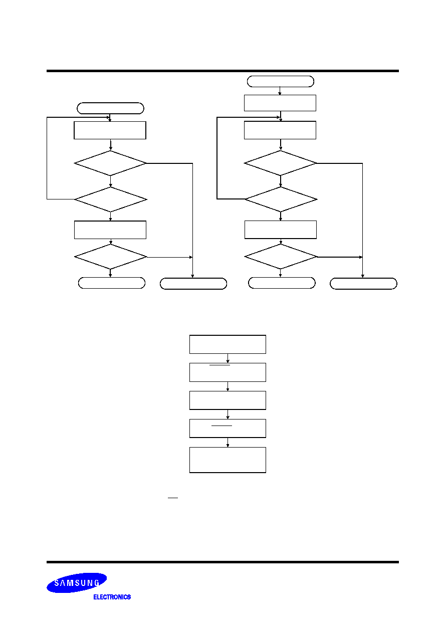
FLASH MEMORY
K8D6x16UTM / K8D6x16UBM
Revision 1.5
March 2005
30
Figure 13. Temporary Block Group Unprotect Routine
Start
RESET=V
ID
Notes :
1. All protected block groups are unprotected.
( If WP/ACC = V
IL
, the two outermost boot blocks remain protected )
2. All previously protected block groups are protected once again.
(Note 1)
Perform Erase or
Program Operations
Temporary Block
Unprotect Completed
(Note 2)
RESET=V
IH
Start
DQ7 = Data ?
No
DQ5 = 1 ?
Fail
Pass
Yes
Figure 11. Data Polling Algorithms
Figure 12. Toggle Bit Algorithms
DQ7 = Data ?
No
No
Yes
Read(DQ0~DQ7)
Valid Address
Read(DQ0~DQ7)
Valid Address
Start
DQ6 = Toggle ?
No
DQ5 = 1 ?
Fail
Pass
No
DQ6 = Toggle ?
Yes
Yes
No
Read twice(DQ0~DQ7)
Valid Address
Read(DQ0~DQ7)
Valid Address
Yes
Yes
Read(DQ0~DQ7)
Valid Address

FLASH MEMORY
K8D6x16UTM / K8D6x16UBM
Revision 1.5
March 2005
31
DC CHARACTERISTICS
RECOMMENDED OPERATING CONDITIONS
( Voltage reference to Vss )
Parameter
Symbol
Min
Typ.
Max
Unit
Supply Voltage
V
CC
2.7
3.0
3.6
V
Supply Voltage
V
SS
0
0
0
V
ABSOLUTE MAXIMUM RATINGS
Notes :
1. Minimum DC voltage is -0.5V on Input/ Output pins. During transitions, this level may fall to -2.0V for periods <20ns. Maximum DC voltage on
input / output pins is Vcc+0.5V which, during transitions, may overshoot to Vcc+2.0V for periods <20ns.
2. Minimum DC voltage is -0.5V on A9, OE, RESET and WP/ACC pins. During transitions, this level may fall to -2.0V for periods <20ns. Maximum DC
voltage on A9, OE, RESET pins is 12.5V which, during transitions, may overshoot to 14.0V for periods <20ns.
3. Permanent device damage may occur if ABSOLUTE MAXIMUM RATINGS are exceeded. Functional operation should be restricted to the conditions
detailed in the operational sections of this data sheet. Exposure to absolute maximum rating conditions for extended periods may affect reliability.
Parameter
Symbol
Rating
Unit
Voltage on any pin relative to V
SS
Vcc
Vcc
-0.5 to +4.0
V
A9, OE , RESET
V
IN
-0.5 to +12.5
WP/ACC
-0.5 to +12.5
All Other Pins
-0.5 to +4.0
Temperature Under Bias
Commercial
T
bias
-10 to +125
∞
C
Industrial
-40 to +125
Storage Temperature
T
stg
-65 to +150
∞
C
Short Circuit Output Current
I
OS
5
mA
Operating Temperature
T
A
(Commercial Temp.)
0 to +70
∞
C
T
A
(Industrial Temp.)
-40 to + 85
∞
C
Parameter
Symbol
Test Conditions
Min
Typ
Max
Unit
Input Leakage Current
I
LI
V
IN
=V
SS
to V
CC
, V
CC
=V
CCmax
-
1.0
-
+
1.0
µ
A
A9,OE,RESET Input Leakage
Current
I
LIT
V
CC
=V
CCmax
, A9,OE,RESET=12.5V
-
-
35
µ
A
WP/ACC Input Leakage Current
I
LIW
V
CC
=V
CCmax
, WP/ACC=12.5V
-
-
35
µ
A
Output Leakage Current
I
LO
V
OUT
=V
SS
to V
CC
,V
CC
=V
CCmax
,OE=V
IH
-
1.0
-
+
1.0
µ
A
Active Read Current (1)
I
CC
1
CE=V
IL
, OE=V
IH
5MHz
-
14
20
mA
1MHz
-
3
6
Active Write Current (2)
I
CC
2
CE=V
IL
, OE=V
IH,
WE=V
IL
-
15
30
mA
Read While Program Current
(3)
I
CC
3
CE=V
IL
, OE=V
IH
-
25
50
mA
Read While Erase Current (3)
I
CC
4
CE=V
IL
, OE=V
IH
-
25
50
mA
Program While Erase Suspend
Current
I
CC
5
CE=V
IL
, OE=V
IH
-
15
35
mA
ACC Accelerated Program
Current
I
ACC
CE=V
IL
, OE=V
IH
ACC Pin
-
5
10
mA
Vcc Pin
-
15
30
Standby Current
I
SB
1
V
CC
=V
CCmax
,CE, RESET=V
CC
±
0.3V
WP/ACC= V
CC
±
0.3V or Vss
±
0.3V
-
10
30
µ
A
Standby Current During Reset
I
SB
2
V
CC
=V
CCmax
, RESET=Vss
±
0.3V,
WP/ACC=V
CC
±
0.3V or Vss
±
0.3V
-
10
30
µ
A
Automatic Sleep Mode
I
SB
3
V
IH
=V
CC
±
0.3V, V
IL
=V
SS
±
0.3V,
OE=V
IL,
I
OL
=I
OH
=0
-
10
30
µ
A
Input Low Level
V
IL
-0.5
-
0.8
V
Input High Level
V
IH
0.7xVcc
-
V
CC
+0.3
V
Voltage for WP/ACC Block Tempo-
rarily Unprotect and Program Accel-
eration (4)
V
HH
V
CC
= 3.0V
±
0.3V
8.5
-
12.5
V
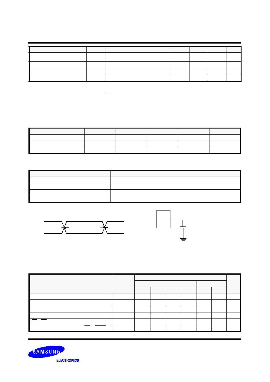
FLASH MEMORY
K8D6x16UTM / K8D6x16UBM
Revision 1.5
March 2005
32
AC CHARACTERISTICS
AC TEST CONDITION
Parameter
Value
Input Pulse Levels
0V to Vcc
Input Rise and Fall Times
5ns
Input and Output Timing Levels
Vcc/2
Output Load
C
L
= 30pF
Read Operations
Note : 1. Not 100% tested.
Parameter
Symbol
V
CC
=2.7V~3.6V
Unit
-7
-8
-9
Min
Max
Min
Max
Min
Max
Read Cycle Time (1)
t
RC
70
-
80
-
90
-
ns
Address Access Time
t
AA
-
70
-
80
-
90
ns
Chip Enable Access Time
t
CE
-
70
-
80
-
90
ns
Output Enable Time
t
OE
-
25
-
25
-
35
ns
CE & OE Disable Time (1)
t
DF
-
16
-
16
-
16
ns
Output Hold Time from Address, CE or OE (1)
t
OH
0
-
0
-
0
-
ns
Notes :
1. The I
CC
current listed includes both the DC operating current and the frequency dependent component(at 5 MHz).
The read current is typically 14 mA (@ VCC=3.0V , OE at VIH.)
2. I
CC
active during Internal Routine(program or erase) is in progress.
3. I
CC
active during Read while Write is in progress.
4. The high voltage ( V
HH
or V
ID
) must be used in the range of Vcc = 3.0V
±
0.3V
5. Not 100% tested.
6. Typical value are measured at Vcc = 3.0V,T
A
=25
∞
C , Not 100% tested.
CAPACITANCE
(T
A
= 25
∞
C, V
CC
= 3.3V, f = 1.0MHz)
Note : Capacitance is periodically sampled and not 100% tested.
Item
Symbol
Test Condition
Min
Max
Unit
Input Capacitance
C
IN
V
IN
=0V
-
10
pF
Output Capacitance
C
OUT
V
OUT
=0V
-
10
pF
Control Pin Capacitance
C
IN2
V
IN
=0V
-
10
pF
Parameter
Symbol
Test Conditions
Min
Typ
Max
Unit
Voltage for Autoselect and
Block Protect (4)
V
ID
V
CC
= 3.0V
±
0.3V
8.5
-
12.5
V
Output Low Level
V
OL
I
OL
=100
µ
A, V
CC
=V
CCmin
-
-
0.4
V
Output High Level
V
OH
I
OH
=-100
µ
A, Vcc = V
CCmin
V
CC
-0.4
-
-
V
Low Vcc Lock-out Voltage (5)
V
LKO
1.8
-
2.5
V
0V
Vcc
Vcc/2
Vcc/2
Input Pulse and Test Point
Input & Output
Test Point
Output Load
*
CL= 30pF including Scope
C
L
Device
and Jig Capacitance
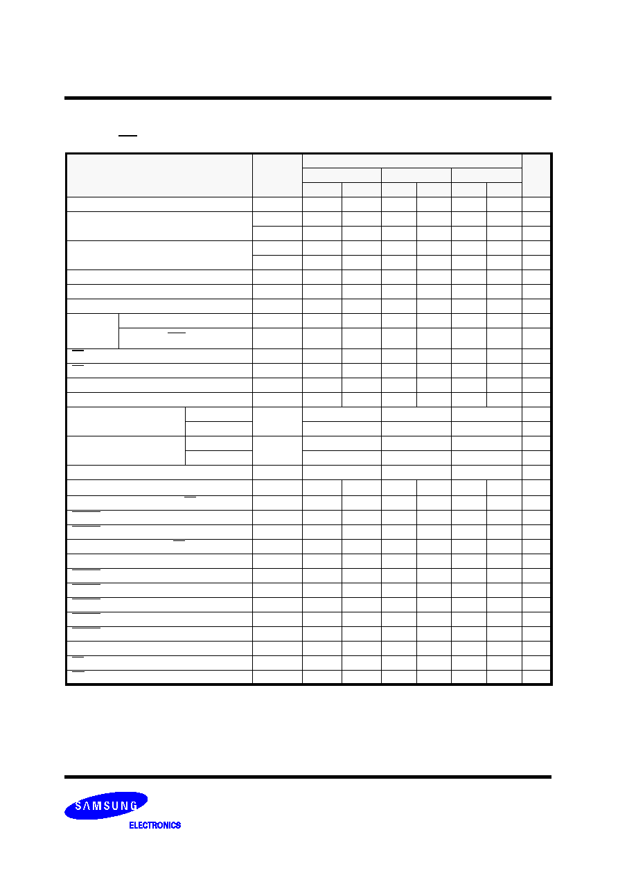
FLASH MEMORY
K8D6x16UTM / K8D6x16UBM
Revision 1.5
March 2005
33
Alternate WE Controlled Write
Notes : 1. Not 100% tested.
2. The duration of the Program or Erase operation varies and is calculated in the internal algorithms.
Parameter
Symbol
V
CC
=2.7V~3.6V
Unit
-7
-8
-9
Min
Max
Min
Max
Min
Max
Write Cycle Time (1)
t
WC
70
-
80
-
90
-
ns
Address Setup Time
t
AS
0
-
0
-
0
-
ns
t
ASO
55
-
55
-
55
-
ns
Address Hold Time
t
AH
45
-
45
-
45
-
ns
t
AHT
0
-
0
-
0
-
ns
Data Setup Time
t
DS
35
-
35
-
45
-
ns
Data Hold Time
t
DH
0
-
0
-
0
-
ns
Output Enable Setup Time (1)
t
OES
0
-
0
-
0
-
ns
Output
Enable
Hold Time
Read (1)
t
OEH1
0
-
0
-
0
-
ns
Toggle and Data Polling (1)
t
OEH2
10
-
10
-
10
-
ns
CE Setup Time
t
CS
0
-
0
-
0
-
ns
CE Hold Time
t
CH
0
-
0
-
0
-
ns
Write Pulse Width
t
WP
35
-
35
-
45
-
ns
Write Pulse Width High
t
WPH
25
-
25
-
30
-
ns
Programming Operation
Word
t
PGM
14(typ.)
14(typ.)
14(typ.)
µ
s
Byte
9(typ.)
9(typ.)
9(typ.)
µ
s
Accelerated Programming
Operation
Word
t
ACCPGM
9(typ.)
9(typ.)
9(typ.)
µ
s
Byte
7(typ.)
7(typ.)
7(typ.)
µ
s
Block Erase Operation (2)
t
BERS
0.7(typ.)
0.7(typ.)
0.7(typ.)
sec
V
CC
Set Up Time
t
VCS
50
-
50
-
50
-
µ
s
Write Recovery Time from RY/BY
t
RB
0
-
0
-
0
-
ns
RESET High Time Before Read
t
RH
50
-
50
-
50
-
ns
RESET to Power Down Time
t
RPD
20
-
20
-
20
-
µ
s
Program/Erase Valid to RY/BY Delay
t
BUSY
90
-
90
-
90
-
ns
V
ID
Rising and Falling Time
t
VID
500
-
500
-
500
-
ns
RESET Pulse Width
t
RP
500
-
500
-
500
-
ns
RESET Low to RY/BY High
t
RRB
-
20
-
20
-
20
µ
s
RESET Setup Time for Temporary Unprotect
t
RSP
1
-
1
-
1
-
µ
s
RESET Low Setup Time
t
RSTS
500
-
500
-
500
-
ns
RESET High to Address Valid
t
RSTW
200
-
200
-
200
-
ns
Read Recovery Time Before Write
t
GHWL
0
-
0
-
0
-
ns
CE High during toggling bit polling
t
CEPH
20
-
20
-
20
-
ns
OE High during toggling bit polling
t
OEPH
20
-
20
-
20
-
ns
AC CHARACTERISTICS
Write(Erase/Program)Operations
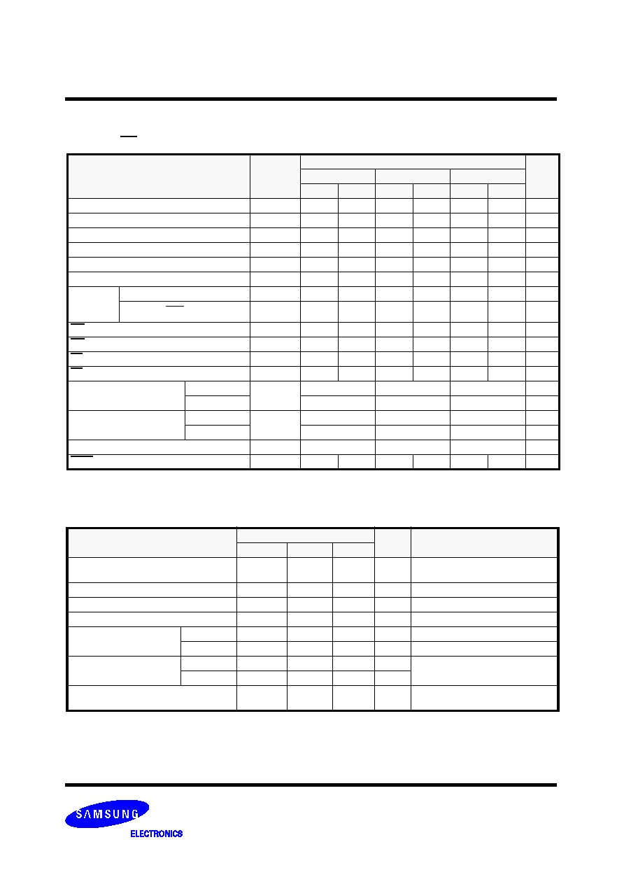
FLASH MEMORY
K8D6x16UTM / K8D6x16UBM
Revision 1.5
March 2005
34
AC CHARACTERISTICS
Write(Erase/Program)Operations
Alternate CE Controlled Writes
Notes :
1. Not 100% tested.
2.This does not include the preprogramming time.
Parameter
Symbol
V
CC
=2.7V~3.6V
Unit
-7
-8
-9
Min
Max
Min
Max
Min
Max
Write Cycle Time (1)
t
WC
70
-
80
-
90
-
ns
Address Setup Time
t
AS
0
-
0
-
0
-
ns
Address Hold Time
t
AH
45
-
45
-
45
-
ns
Data Setup Time
t
DS
35
-
35
-
45
-
ns
Data Hold Time
t
DH
0
-
0
-
0
-
ns
Output Enable Setup Time (1)
t
OES
0
-
0
-
0
-
ns
Output
Enable
Hold Time
Read (1)
t
OEH1
0
-
0
-
0
-
ns
Toggle and Data Polling (1)
t
OEH2
10
-
10
-
10
-
ns
WE Setup Time
t
WS
0
-
0
-
0
-
ns
WE Hold Time
t
WH
0
-
0
-
0
-
ns
CE Pulse Width
t
CP
35
-
35
-
45
-
ns
CE Pulse Width High
t
CPH
25
-
25
-
30
-
ns
Programming Operation
Word
t
PGM
14(typ.)
14(typ.)
14(typ.)
µ
s
Byte
9(typ.)
9(typ.)
9(typ.)
µ
s
Accelerated Programming
Operation
Word
t
ACCPGM
9(typ.)
9(typ.)
9(typ.)
µ
s
Byte
7(typ.)
7(typ.)
7(typ.)
µ
s
Block Erase Operation (2)
t
BERS
0.7(typ.)
0.7(typ.)
0.7(typ.)
sec
BYTE Switching Low to Output HIGH-Z
t
FLQZ
25
-
25
-
30
-
ns
ERASE AND PROGRAM PERFORMANCE
Notes : 1. 25
∞
C, V
CC
=
3.0V 100,000 cycles, typical pattern
.
2. System-level overhead is defined as the time required to execute the four bus cycle command necessary to program each byte.
In the preprogramming step of the Internal Erase Routine, all bytes are programmed to 00H before erasure.
Parameter
Limits
Unit
Comments
Min
Typ
Max
Block Erase Time
-
0.7
15
sec
Excludes 00H programming
prior to erasure
Chip Erase Time
-
98
-
sec
Word Programming Time
-
14
330
µ
s
Excludes system-level overhead
Byte Programming Time
-
9
210
µ
s
Excludes system-level overhead
Accelerated Byte/Word
Program Time
Word Mode
-
9
210
µ
s
Excludes system-level overhead
Byte Mode
-
7
150
µ
s
Excludes system-level overhead
Chip Programming Time
Word Mode
-
59
177
sec
Excludes system-level overhead
Byte Mode
-
75
225
sec
Erase/Program Endurance
100,000
-
-
cycles
Minimum 100,000 cycles guaran-
teed
FLASH MEMORY
K8D6x16UTM / K8D6x16UBM
Revision 1.5
March 2005
35
Read Operations
SWITCHING WAVEFORMS
OE
Address
t
CE
t
OEH1
CE
Outputs
WE
HIGH-Z
Output Valid
t
RC
Address Stable
t
AA
t
OE
t
OH
HIGH-Z
t
DF
RY/BY
HIGH
Note :
1. Not 100% tested.
Parameter
Symbol
-7
-8
-9
Unit
Min
Max
Min
Max
Min
Max
Read Cycle Time
t
RC
70
-
80
-
90
-
ns
Address Access Time
t
AA
-
70
-
80
-
90
ns
Chip Enable Access Time
t
CE
-
70
-
80
-
90
ns
Output Enable Time
t
OE
-
25
-
25
-
35
ns
CE & OE Disable Time (1)
t
DF
-
16
-
16
-
16
ns
Output Hold Time from Address, CE or OE
t
OH
0
-
0
-
0
-
ns
OE Hold Time
t
OEH1
0
-
0
-
0
-
ns
FLASH MEMORY
K8D6x16UTM / K8D6x16UBM
Revision 1.5
March 2005
36
Hardware Reset/Read Operations
SWITCHING WAVEFORMS
Parameter
Symbol
-7
-8
-9
Unit
Min
Max
Min
Max
Min
Max
Read Cycle Time
t
RC
70
-
80
-
90
-
ns
Address Access Time
t
AA
-
70
-
80
-
90
ns
Chip Enable Access Time
t
CE
-
70
-
80
-
90
ns
Output Hold Time from Address, CE or OE
t
OH
0
-
0
-
0
-
ns
RESET Pulse Width
t
RP
500
-
500
-
500
-
ns
RESET High Time Before Read
t
RH
50
-
50
-
50
-
ns
RESET
Address
CE
Outputs
High-Z
t
RC
Address Stable
t
AA
t
CE
t
OH
t
RH
t
RH
t
RP
Output Valid
FLASH MEMORY
K8D6x16UTM / K8D6x16UBM
Revision 1.5
March 2005
37
Alternate WE Controlled Program Operations
SWITCHING WAVEFORMS
Notes : 1. DQ7 is the output of the complement of the data written to the device.
2. DOUT is the output of the data written to the device.
3. PA : Program Address, PD : Program Data
4. The illustration shows the last two cycles of the program command sequence.
OE
Address
t
CS
CE
DATA
WE
t
AH
t
OH
t
DF
t
AS
t
RC
t
OE
t
CE
t
DS
t
DH
t
WP
t
OES
t
PGM
Status
DOUT
555H
PA
PA
A0H
Data Polling
t
CH
PD
t
WPH
RY/BY
t
BUSY
t
RB
t
WC
Parameter
Symbol
-7
-8
-9
Unit
Min
Max
Min
Max
Min
Max
Write Cycle Time
t
WC
70
-
80
-
90
-
ns
Address Setup Time
t
AS
0
-
0
-
0
-
ns
Address Hold Time
t
AH
45
-
45
-
45
-
ns
Data Setup Time
t
DS
35
-
35
-
45
-
ns
Data Hold Time
t
DH
0
-
0
-
0
-
ns
CE Setup Time
t
CS
0
-
0
-
0
-
ns
CE Hold Time
t
CH
0
-
0
-
0
-
ns
OE Setup Time
t
OES
0
-
0
-
0
-
ns
Write Pulse Width
t
WP
35
-
35
-
45
-
ns
Write Pulse Width High
t
WPH
25
-
25
-
30
-
ns
Programming Operation
Word
t
PGM
14(typ.)
14(typ.)
14(typ.)
us
Byte
9(typ.)
9(typ.)
9(typ.)
us
Accelerated Programming
Operation
Word
t
ACCPGM
9(typ.)
9(typ.)
9(typ.)
µ
s
Byte
7(typ.)
7(typ.)
7(typ.)
µ
s
Read Cycle Time
t
RC
70
-
80
-
90
-
ns
Chip Enable Access Time
t
CE
-
70
-
80
-
90
ns
Output Enable Time
t
OE
-
25
-
25
-
35
ns
CE & OE Disable Time
t
DF
-
16
-
16
-
16
ns
Output Hold Time from Address, CE or OE
t
OH
0
-
0
-
0
-
ns
Program/Erase Valide to RY/BY Delay
t
BUSY
90
-
90
-
90
-
ns
Recovery Time from RY/BY
t
RB
0
-
0
-
0
-
ns
FLASH MEMORY
K8D6x16UTM / K8D6x16UBM
Revision 1.5
March 2005
38
Alternate CE Controlled Program Operations
SWITCHING WAVEFORMS
Notes :
1. DQ7 is the output of the complement of the data written to the device.
2. DOUT is the output of the data written to the device.
3. PA : Program Address, PD : Program Data
4. The illustration shows the last two cycles of the program command sequence.
OE
Address
WE
DATA
CE
t
AH
t
AS
t
DS
t
DH
t
CP
t
OES
A0H
555H
PA
PA
Status
DOUT
Data Polling
t
CPH
t
WS
t
PGM
RY/BY
t
BUSY
t
RB
PD
t
WC
Parameter
Symbol
-7
-8
-9
Unit
Min
Max
Min
Max
Min
Max
Write Cycle Time
t
WC
70
-
80
-
90
-
ns
Address Setup Time
t
AS
0
-
0
-
0
-
ns
Address Hold Time
t
AH
45
-
45
-
45
-
ns
Data Setup Time
t
DS
35
-
35
-
45
-
ns
Data Hold Time
t
DH
0
-
0
-
0
-
ns
OE Setup Time
t
OES
0
-
0
-
0
-
ns
WE Setup Time
t
WS
0
-
0
-
0
-
ns
WE Hold Time
t
WH
0
-
0
-
0
-
ns
CE Pulse Width
t
CP
35
-
35
-
45
-
ns
CE Pulse Width High
t
CPH
25
-
25
-
30
-
ns
Programming Operation
Word
t
PGM
14(typ.)
14(typ.)
14(typ.)
µ
s
Byte
9(typ.)
9(typ.)
9(typ.)
µ
s
Accelerated Programming
Operation
Word
t
ACCPGM
9(typ.)
9(typ.)
9(typ.)
µ
s
Byte
7(typ.)
7(typ.)
7(typ.)
µ
s
Program/Erase Valide to RY/BY Delay
t
BUSY
90
-
90
-
90
-
ns
Recovery Time from RY/BY
t
RB
0
-
0
-
0
-
ns
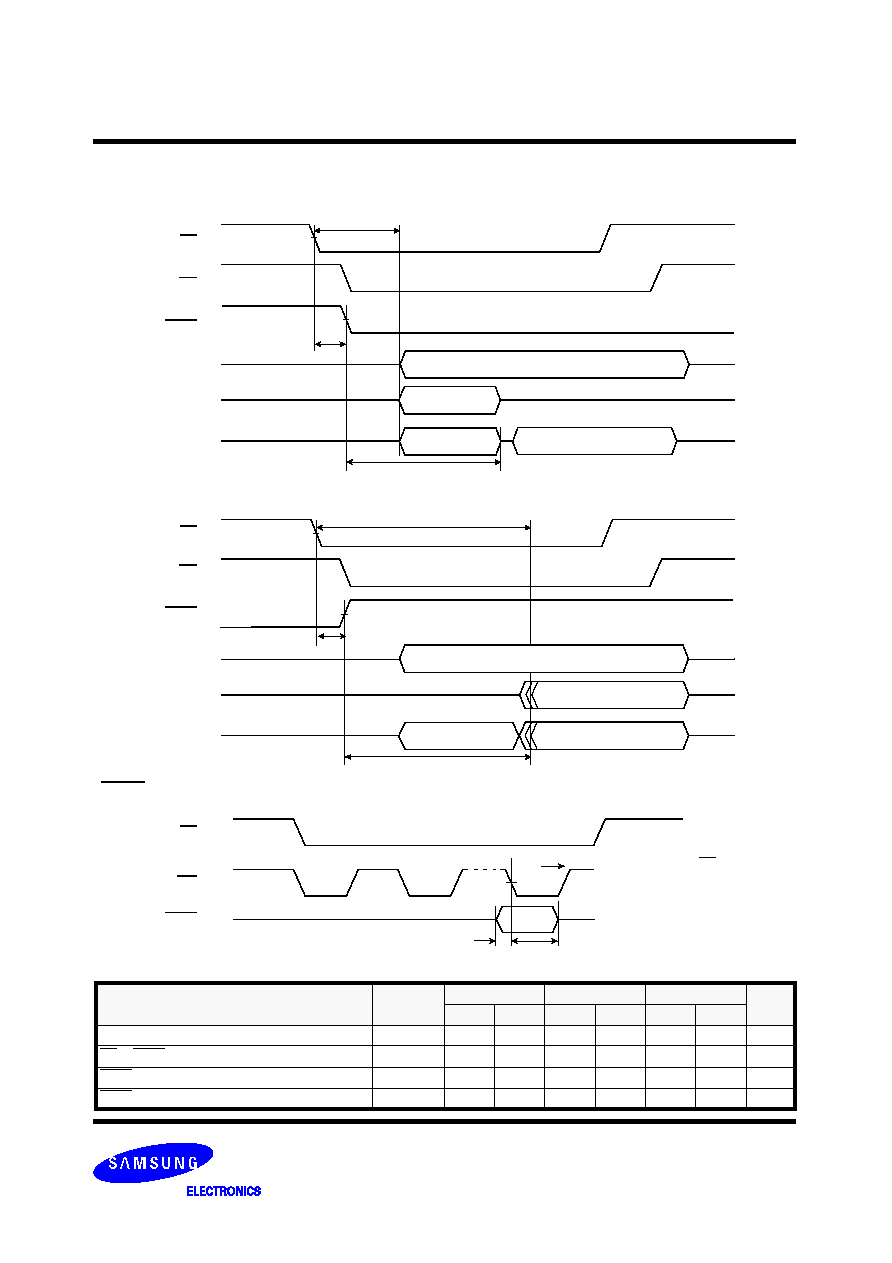
FLASH MEMORY
K8D6x16UTM / K8D6x16UBM
Revision 1.5
March 2005
39
SWITCHING WAVEFORMS
Parameter
Symbol
-7
-8
-9
Unit
Min
Max
Min
Max
Min
Max
Chip Enable Access Time
t
CE
-
70
-
80
-
90
ns
CE to BYTE Switching Low or High
t
ELFL
/t
ELFH
-
5
-
5
-
5
ns
BYTE Switching Low to Output HIGH-Z
t
FLQZ
-
25
-
25
-
30
ns
BYTE Switching High to Output Active
t
FHQV
-
25
-
25
-
35
ns
OE
t
FLQZ
CE
DQ0-DQ7
BYTE
WE
BYTE Timing Diagram for Write Operation
The falling edge of the last WE signal
CE
BYTE
t
HOLD
(t
AH
)
DQ15/A-1
t
ELFL
Address Input (A-1)
t
SET
(t
AS
)
Word to Byte Timing Diagram for Read Operation
Byte to Word Timing Diagram for Read Operation
Data Output
(DQ0-DQ7)
DQ8-DQ14
Data Output
(DQ8-DQ14)
Data Output
(DQ15)
OE
t
FHQV
CE
DQ0-DQ7
BYTE
DQ15/A-1
t
ELFH
Data Output
DQ8-DQ14
Address Input
(A-1)
Data Output
(DQ8-DQ14)
(DQ15)
t
CE
t
CE
Data Output
(DQ0-DQ7)
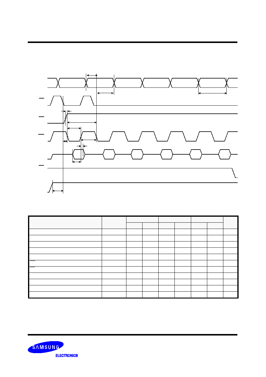
FLASH MEMORY
K8D6x16UTM / K8D6x16UBM
Revision 1.5
March 2005
40
SWITCHING WAVEFORMS
Chip/Block Erase Operations
Parameter
Symbol
-7
-8
-9
Unit
Min
Max
Min
Max
Min
Max
Write Cycle Time
t
WC
70
-
80
-
90
-
ns
Address Setup Time
t
AS
0
-
0
-
0
-
ns
Address Hold Time
t
AH
45
-
45
-
45
-
ns
Data Setup Time
t
DS
35
-
35
-
45
-
ns
Data Hold Time
t
DH
0
-
0
-
0
-
ns
OE Setup Time
t
OES
0
-
0
-
0
-
ns
CE Setup Time
t
CS
0
-
0
-
0
-
ns
Write Pulse Width
t
WP
35
-
35
-
45
-
ns
Write Pulse Width High
t
WPH
25
-
25
-
30
-
ns
Read Cycle Time
t
RC
70
-
80
-
90
-
ns
V
CC
Set Up Time
t
VCS
50
-
50
-
50
-
µ
s
OE
Address
t
CS
CE
DATA
WE
t
AH
t
AS
t
RC
t
DS
t
DH
80H
AAH
AAH
55H
30H
10H for Chip Erase
555H
2AAH
555H
555H
2AAH
BA
555H for Chip Erase
t
WPH
t
WP
t
OES
55H
RY/BY
t
WC
t
VCS
Vcc
Note : BA : Block Address
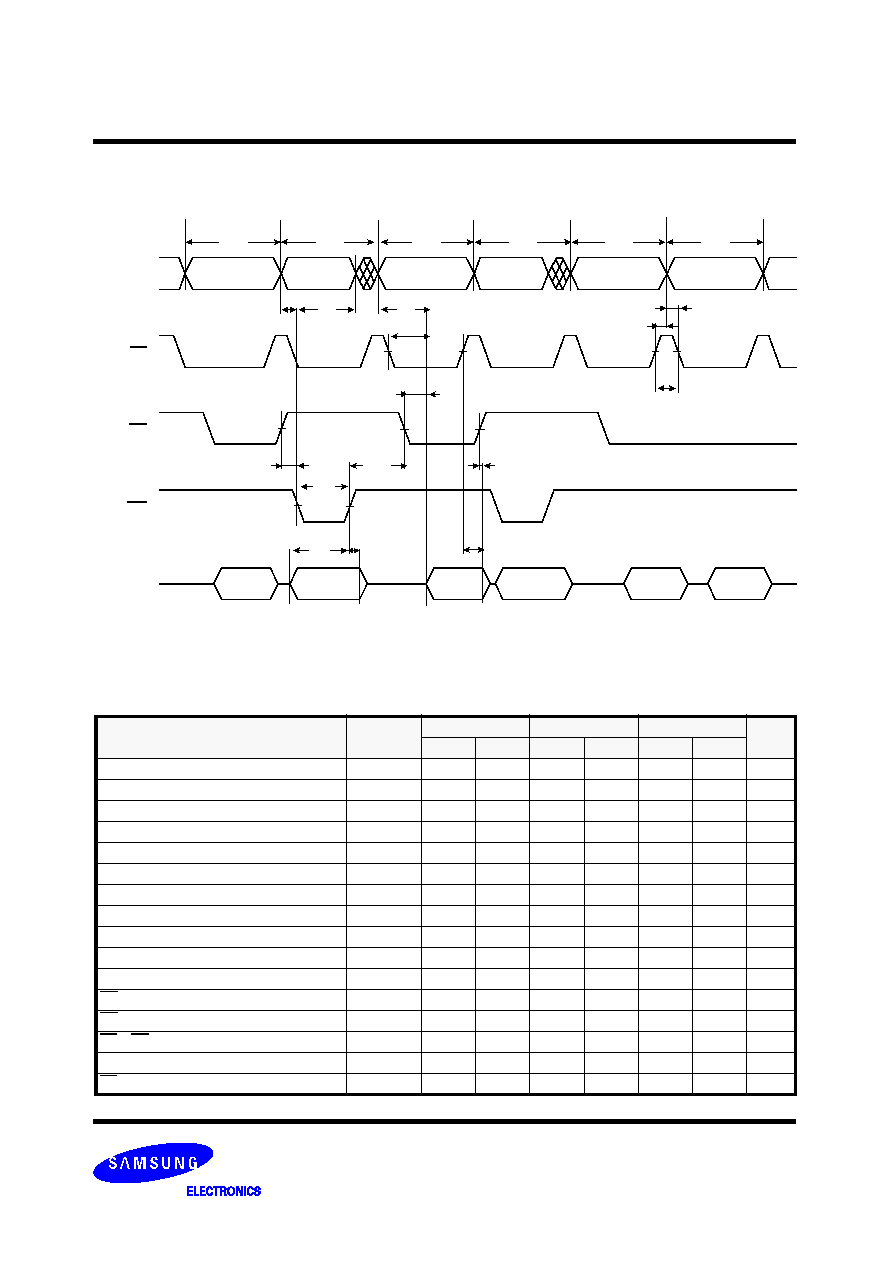
FLASH MEMORY
K8D6x16UTM / K8D6x16UBM
Revision 1.5
March 2005
41
Read While Write Operations
SWITCHING WAVEFORMS
Parameter
Symbol
-7
-8
-9
Unit
Min
Max
Min
Max
Min
Max
Write Cycle Time
t
WC
70
-
80
-
90
-
ns
Write Pulse Width
t
WP
35
-
35
-
45
-
ns
Write Pulse Width High
t
WPH
25
-
25
-
30
-
ns
Address Setup Time
t
AS
0
-
0
-
0
-
ns
Address Hold Time
t
AH
45
-
45
-
45
-
ns
Data Setup Time
t
DS
35
-
35
-
45
-
ns
Data Hold Time
t
DH
0
-
0
-
0
-
ns
Read Cycle Time
t
RC
70
-
80
-
90
-
ns
Chip Enable Access Time
t
CE
-
70
-
80
-
90
ns
Address Access Time
t
AA
-
70
-
80
-
90
ns
Output Enable Access Time
t
OE
-
25
-
25
-
35
ns
OE Setup Time
t
OES
0
-
0
-
0
-
ns
OE Hold Time
t
OEH2
10
-
10
-
10
-
ns
CE & OE Disable Time
t
DF
-
16
-
16
-
16
ns
Address Hold Time
t
AHT
0
-
0
-
0
-
ns
CE High during toggle bit polling
t
CEPH
20
-
20
-
20
-
ns
Note : This is an example in the program-case of the Read While Write function.
DA1 : Address of Bank1, DA2 : Address of Bank 2
PA = Program Address at one bank , RA = Read Address at the other bank, PD = Program Data In , RD = Read Data Out
OE
CE
DQ
WE
t
RC
Read
Command
Command
Read
Read
Read
t
AH
t
AA
t
CE
t
AS
t
AHT
t
AS
t
CEPH
t
OE
t
OES
t
WP
t
OEH2
t
DF
t
DS
t
DH
t
DF
DA1
DA2
DA1
DA1
DA2
DA2
(555H)
(PA)
(PA)
Valid
Output
Valid
Output
Valid
Input
Valid
Output
Valid
Input
Status
Address
(A0H)
(PD)
t
RC
t
RC
t
RC
t
WC
t
WC
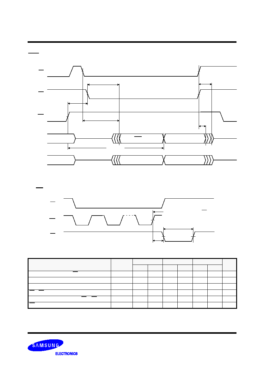
FLASH MEMORY
K8D6x16UTM / K8D6x16UBM
Revision 1.5
March 2005
42
Data Polling During Internal Routine Operation
SWITCHING WAVEFORMS
Parameter
Symbol
-7
-8
-9
Unit
Min
Max
Min
Max
Min
Max
Program/Erase Valid to RY/BY Delay
t
BUSY
90
-
90
-
90
-
ns
Chip Enable Access Time
t
CE
-
70
-
80
-
90
ns
Output Enable Time
t
OE
-
25
-
25
-
35
ns
CE & OE Disable Time
t
DF
-
16
-
16
-
16
ns
Output Hold Time from Address, CE or OE
t
OH
0
-
0
-
0
-
ns
OE Hold Time
t
OEH2
10
-
10
-
10
-
ns
OE
t
CE
t
OEH2
CE
DQ7
WE
t
OE
HIGH-Z
t
DF
Note : *DQ7=Vaild Data (The device has completed the internal operation).
DQ7
*DQ7 = Valid Data
t
OH
t
PGM
or t
BERS
HIGH-Z
Valid Data
DQ0-DQ6
Data In
Data In
WE
RY/BY Timing Diagram During Program/Erase Operation
The rising edge of the last WE signal
CE
RY/BY
t
BUSY
Entire progrming
or erase operation
Status Data

FLASH MEMORY
K8D6x16UTM / K8D6x16UBM
Revision 1.5
March 2005
43
Toggle Bit During Internal Routine Operation
SWITCHING WAVEFORMS
t
DH
CE
Address*
OE
DQ6/DQ2
WE
RY/BY
Data In
t
AHT
t
AHT
t
ASO
t
AS
t
CEPH
t
OEH2
t
OEPH
Status
Data
t
OE
Status
Data
Status
Data
Array Data Out
Note : Address for the write operation must include a bank address (A20~A21) where the data is written.
DQ
6
WE
DQ
2
Enter
Embedded
Erasing
Erase
Suspend
Enter Erase
Suspend Program
Erase
Suspend
Program
Erase
Resume
Erase
Erase Suspend
Read
Erase
Erase
Complete
Erase Suspend
Read
Note : DQ2 is read from the erase-suspended block.
Toggle
DQ
2
and DQ
6
with OE or CE
Parameter
Symbol
-7
-8
-9
Unit
Min
Max
Min
Max
Min
Max
Output Enable Access Time
t
OE
-
25
-
25
-
35
ns
OE Hold Time
t
OEH2
10
-
10
-
10
-
ns
Address Hold Time
t
AHT
0
-
0
-
0
-
ns
Address Setup
t
ASO
55
-
55
-
55
-
ns
Address Setup Time
t
AS
0
-
0
-
0
-
ns
Data Hold Time
t
DH
0
-
0
-
0
-
ns
CE High during toggle bit polling
t
CEPH
20
-
20
-
20
-
ns
OE High during toggle bit polling
t
OEPH
20
-
20
-
20
-
ns
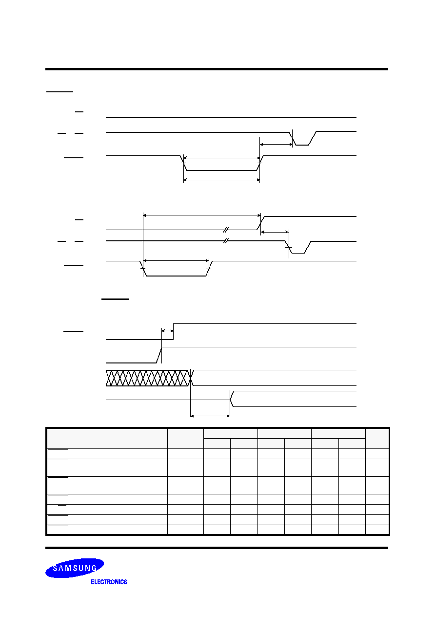
FLASH MEMORY
K8D6x16UTM / K8D6x16UBM
Revision 1.5
March 2005
44
RESET Timing Diagram
SWITCHING WAVEFORMS
Parameter
Symbol
-7
-8
-9
Unit
Min
Max
Min
Max
Min
Max
RESET Pulse Width
t
RP
500
-
500
-
500
-
ns
RESET Low to Valid Data
(During Internal Routine)
t
READY
-
20
-
20
-
20
µ
s
RESET Low to Valid Data
(Not during Internal Routine)
t
READY
-
500
-
500
-
500
ns
RESET High Time Before Read
t
RH
50
-
50
-
50
-
ns
RY/BY Recovery Time
t
RB
0
-
0
-
0
-
ns
RESET High to Address Valid
t
RSTW
200
-
200
-
200
-
ns
RESET Low Set-up Time
t
RSTS
500
-
500
-
500
-
ns
RESET
t
RP
Power-up and RESET Timing Diagram
CE or OE
RY/BY
t
READY
t
RB
RESET
CE or OE
RY/BY
t
RH
t
READY
t
RP
Reset Timings NOT during Internal Routine
Reset Timings during Internal Routine
High
RESET
t
AA
Vcc
Address
DATA
t
RSTS
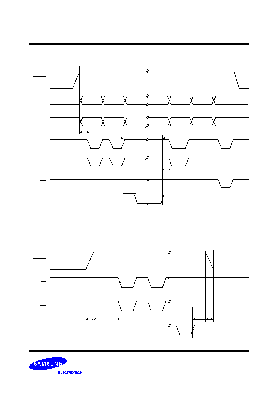
FLASH MEMORY
K8D6x16UTM / K8D6x16UBM
Revision 1.5
March 2005
45
Block Group Protect & Unprotect Operations
SWITCHING WAVEFORMS
CE
Temporary Block Group Unprotect
Program or Erase Command Sequence
RESET
WE
t
RSP
RY/BY
t
VID
V
ID
V
ss
,V
IL
,
or V
IH
V
ss
,V
IL
,
or V
IH
t
RRB
t
VID
BGA,A6
A1,A0
RESET
CE
WE
DATA
OE
V
ss
,V
IL
,
60H
60H
40H
Status*
Block Group Protect / Unprotect
Verify
1
µ
s
Block Group Protect:150
µ
s
Block Group UnProtect:15ms
Notes : Block Group Protect (A6=
V
IL
, A1=
V
IH
, A0=
V
IL
) , Status=01H
Block Group Unprotect (A6=
V
IH
, A1=
V
IH
,
A0=
V
IL
) , Status=00H
BGA = Block Group Address (A12 ~ A21)
RY/BY
V
ID
Valid
Valid
Valid
t
BUSY
t
RB
or V
IH
V
ss
,V
IL
,
or V
IH

FLASH MEMORY
K8D6x16UTM / K8D6x16UBM
Revision 1.5
March 2005
46
PACKAGE DIMENSIONS
48-Ball Tape Ball Grid Array Package (measured in millimeters)
Side View
0.45
±
0.05
0.08MAX
0.
3
2
±
0.0
5
0.
9
0
±
0.1
0
9.00
±
0.10
Top View
Bottom View
#A1
A
B
C
E
G
D
F
H
0.80 x 5=4.00
A
0.
80x7=5.
60
2.00
48-
0.45
±
0.05
2.
8
0
0.
80
0.20
M
A B
(Datum A)
(Datum B)
0.80
9.
00
±
0.
10
6.00
±
0.10
B
1
4
2
6
5
3
9.
00
±
0.
10
6.00
±
0.10
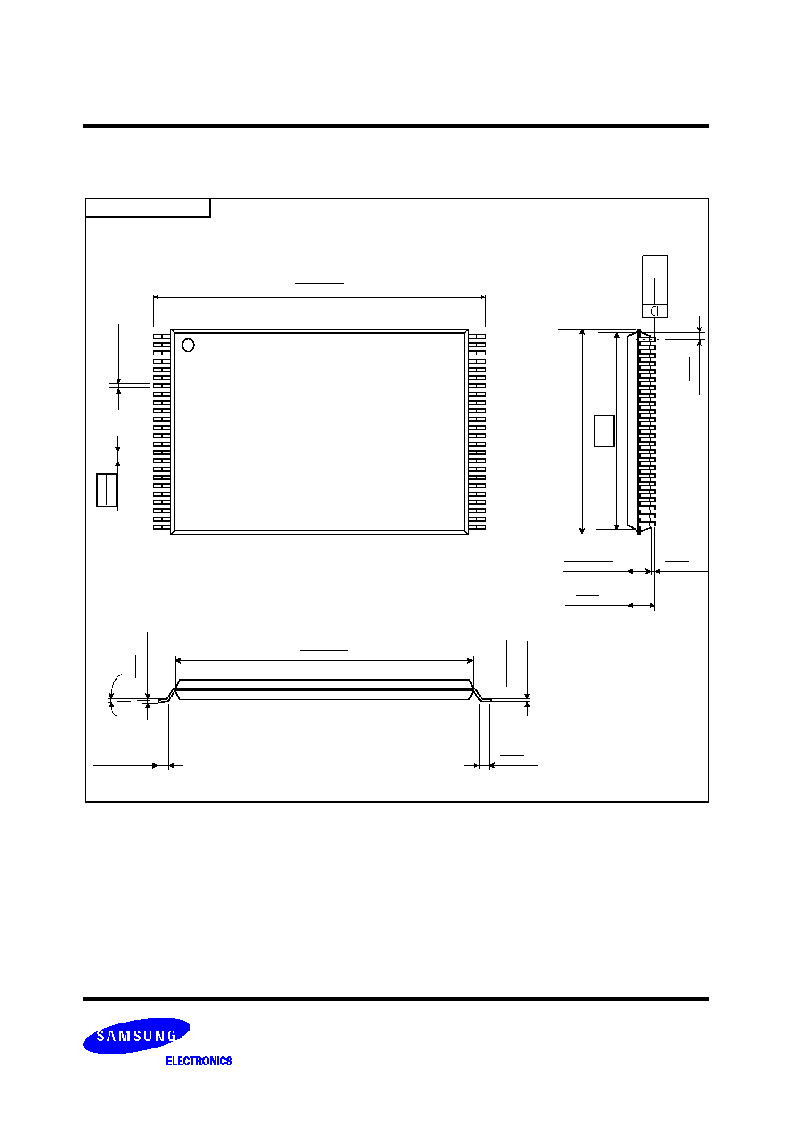
FLASH MEMORY
K8D6x16UTM / K8D6x16UBM
Revision 1.5
March 2005
47
PACKAGE DIMENSIONS
48-PIN LEAD PLASTIC THIN SMALL OUT-LINE PACKAGE TYPE(I)
48 - TSOP1 - 1220F
Unit :mm/Inch
0.787
±
0.008
20.00
±
0.20
#1
#24
0.
2
0
+0
.07
-0
.0
3
0.
008
+0
.003
-
0
.001
0.
5
0
0.
019
7
#48
#25
0.
4
8
8
12
.
4
0
MAX
12
.
0
0
0.
4
7
2
0.
10
0.
00
4
MAX
0.
25
0.
01
0
()
0.039
±
0.002
1.00
±
0.05
0.002
0.05
MIN
0.047
1.20
MAX
0.45~0.75
0.018~0.030
0.724
±
0.004
18.40
±
0.10
0~8'C
0.
0
1
0
0.
25
TYP
0.
12
5
+0
.075
-
0
.035
0.
005
+
0
.003
-0
.0
0
1
0.50
0.020
(
)
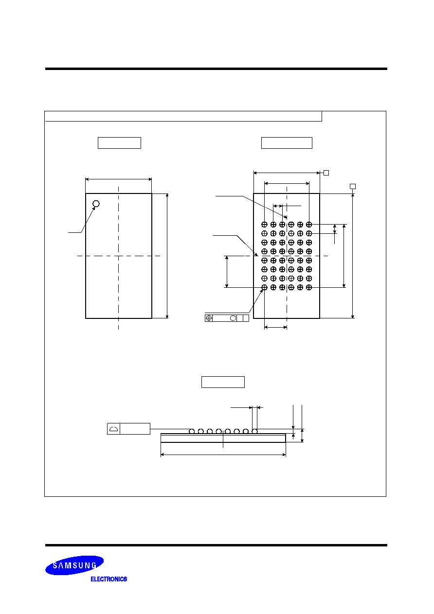
FLASH MEMORY
K8D6x16UTM / K8D6x16UBM
Revision 1.5
March 2005
48
PACKAGE DIMENSIONS
48-Ball Fine Ball Grid Array Package (measured in millimeters)
Side View
0.45
±
0.05
0.08MAX
0.
3
2
±
0.0
5
0.
9
0
±
0.1
0
9.00
±
0.10
Top View
Bottom View
#A1
A
B
C
E
G
D
F
H
0.80 x 5=4.00
A
0.
80x7=5.
60
2.00
48-
0.45
±
0.05
2.
8
0
0.
80
0.20
M
A B
(Datum A)
(Datum B)
0.80
9.
00
±
0.
10
6.00
±
0.10
B
1
4
2
6
5
3
9.
00
±
0.
10
6.00
±
0.10