K9F1208U0M-YCB0, K9F1208U0M-YIB0
FLASH MEMORY
1
Document Title
64M x 8 Bit NAND Flash Memory
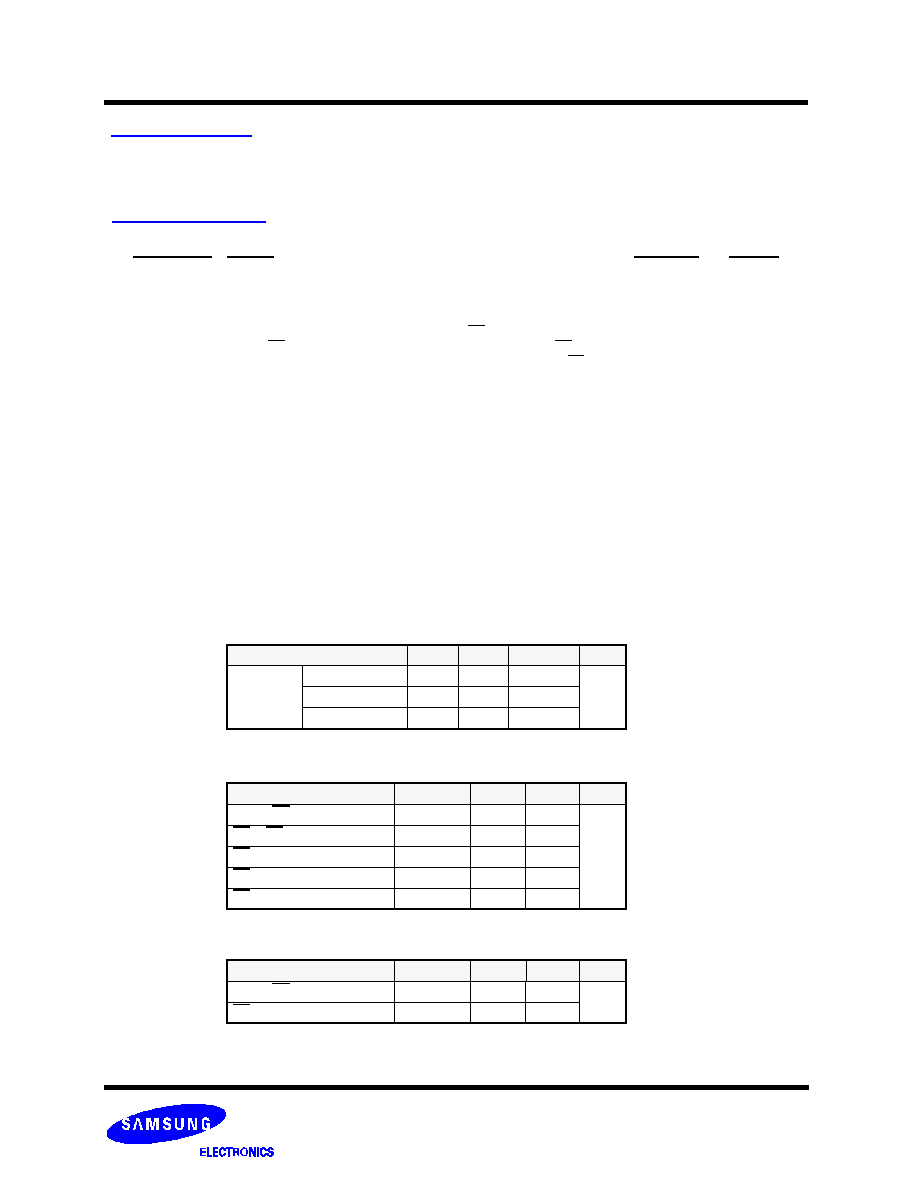
Revision History
Revision No
0.0
0.1
0.2
0.3
0.4
Remark
Advanced
Information
History
1. Initial issue
1. Renamed GND input (pin # 6) on behalf of SE (pin # 6)
- The SE input controls the access of the spare area. When SE is high,
the spare area is not accessible for reading or programming. SE is rec
ommended to be coupled to GND or Vcc and should not be toggled
during reading or programming.
=> Connect this input pin to GND or set to static low state unless the
sequential read mode excluding spare area is used.
2. Updated operation for tRST timing
- If reset command(FFh) is written at Ready state, the device goes into
Busy for maximum 5us.
1. Changed GND input (pin # 6) pin to N.C ( No Connection).
- The pin # 6 is don't-cared regardless of external logic input level
and is fixed as low internally.
1. Changed plane address in Copy-Back Program
-
A24 and A25
must be the same between source and target page
=>
A14 and A15
must be the same between source and target page
1. Changed DC characteristics
2. Unified access timing parameter definition for multiple operating modes
- Changed AC characteristics (Before)
- AC characteristics (After)
. Deleted t
CR
,t
RSTO,
t
CSTO
and t
READID
/ Added t
CEA
Parameter
Min
Typ
Max
Unit
Operating
Current
Sequential Read
-
10
20->30
mA
Program
-
10
20->30
Erase
-
10
20->30
Parameter
Symbol
Min
Max
Unit
ALE to RE Delay( ID read )
t
AR1
100
-
ns
CE to RE Delay( ID read)
t
CR
100
-
RE Low to Status Output
t
RSTO
-
35
CE Low to Status Output
t
CSTO
-
45
RE access time(Read ID)
t
READID
-
35
Parameter
Symbol
Min
Max
Unit
ALE to RE Delay( ID read )
t
AR1
10
-
ns
CE Access Time
t
CEA
-
45
Draft Date
Oct. 27th 2000
Dec. 5th 2000
Dec. 15th 2000
Jan. 8th 2001
Apr. 7th 2001

K9F1208U0M-YCB0, K9F1208U0M-YIB0
FLASH MEMORY
2
The attached data sheets are prepared and approved by SAMSUNG Electronics. SAMSUNG Electronics CO., LTD. reserve the
right to change the specifications. SAMSUNG Electronics will evaluate and reply to your requests and questions about device. If you
have any questions, please contact the SAMSUNG branch office near your office.
Revision History
Revision No
Remark
History
Draft Date
CE
CLE
I/O
0
~
7
ALE
RE
WE
90h
00h
ECh
Address. 1cycle
Maker code
tCEA
tAR1
tREA
tWHR
CE
CLE
I/O
0
~
7
ALE
RE
WE
90h
00h
ECh
Address. 1cycle
Maker code
tCR
tAR1
tREA
CE
WE
CLE
RE
I/O
0
~
7
70h
Status Output
tCLS
tCLH
tCS
tWP
tCH
tDS
tDH
tRSTO
tIR
tRHZ*
tCHZ*
tWHR
tCSTO
tCLS
CE
WE
CLE
RE
I/O
0
~
7
70h
Status Output
tCLS
tCLH
tCS
tWP
tCH
tDS
tDH
tREA
tIR
tRHZ*
tCHZ*
tWHR
tCEA
tCLS

K9F1208U0M-YCB0, K9F1208U0M-YIB0
FLASH MEMORY
3
Revision No
0.5
0.6
0.7
Remark
Preliminary
History
1. Addition of new operation : Multi-Plane Copy-Back Program.
- Multi-Plane Copy-Back Program is extended operation of one-page
Copy-Back program.
=> After successive reading of multiple 528 byte data set at the source
planes, the above data are moved to internal page registers and same
procedure as Multi-Plane Page Programming is executed.
1.Powerup sequence is added
: Recovery time of minimum 1
�
s is required before internal circuit gets
ready for any command sequences
2. AC parameter tCLR(CLE to RE Delay, min 50ns) is added.
1. Copy-Back Program(Dummy) is added in Command sets table.
(before revision)
(after revision)
Note 2. Page Program(True) and Copy-Back Program(True) are available on 1 plane
operation.
Page Program(Dummy) and Copy-Back Program(Dummy) are available on
the 2nd,3rd,4th plane of multi plane operation.
Function
1st.
Cycle
2nd.
Cycle
3rd.
Cycle
Page Program (True)
80h
10h
-
Page Program (Dummy)
80h
11h
-
Copy-Back Program(True)
00h
8Ah
10h
Function
1st.
Cycle
2nd.
Cycle
3rd.
Cycle
Page Program (True)
(2)
80h
10h
-
Page Program (Dummy)
(2)
80h
11h
-
Copy-Back Program(True)
(2)
00h
8Ah
10h
Copy-Back Program(Dummy)
(2)
03h
8Ah
11h/10h
1
�
s
V
CC
WP
High
~ 2.5V
~ 2.5V
WE
Draft Date
May. 30th 2001
Jul. 23th 2001
Aug. 23th 2001

K9F1208U0M-YCB0, K9F1208U0M-YIB0
FLASH MEMORY
4
Revision No
0.8
Remark
History
1. In Read ID & Status Read timing diagram, tCLS is changed to tCLR.
Draft Date
Oct. 7th 2001
CE
CLE
I/O
0
~
7
ALE
RE
WE
90h
00h
ECh
Address. 1cycle
Maker code
tCEA
tAR1
tREA
tWHR
CE
WE
CLE
RE
I/O
0
~
7
70h
Status Output
tCLS
tCLH
tCS
tWP
tCH
tDS
tDH
tREA
tIR
tRHZ*
tCHZ*
tWHR
tCEA
tCLS
CE
CLE
I/O
0
~
7
ALE
RE
WE
90h
00h
ECh
Address. 1cycle
Maker code
tCEA
tAR1
tREA
tWHR
CE
WE
CLE
RE
I/O
0
~
7
70h
Status Output
tCLR
tCLH
tCS
tWP
tCH
tDS
tDH
tREA
tIR
tRHZ*
tCHZ*
tWHR
tCEA
tCLS
tCLS
tCLR

K9F1208U0M-YCB0, K9F1208U0M-YIB0
FLASH MEMORY
5
Revision No
0.9
Remark
History
To clarify the meaning of parameter,
1. tRHZ is devide into tRHZ and tOH.(page 12)
- tRHZ : RE High to Output Hi-Z
- tOH : RE High to Output Hold
2. tCHZ is devide into tCHZ and tOH.(page 12)
- tCHZ : CE High to Output Hi-Z
- tOH : CE High to Output Hold
Draft Date
Apr. 20th 2002