
FLASH MEMORY
1
K9F1208D0A
K9F1208U0A
K9F1216D0A
K9F1216U0A
Document Title
64M x 8 Bit , 32M x 16 Bit NAND Flash Memory
Revision History
The attached datasheets are prepared and approved by SAMSUNG Electronics. SAMSUNG Electronics CO., LTD. reserve the right
to change the specifications. SAMSUNG Electronics will evaluate and reply to your requests and questions about device. If you have
any questions, please contact the SAMSUNG branch office near you.
Revision No.
0.0
0.1
0.2
0.3
0.4
0.5
0.6
0.7
0.8
0.9
1.0
Remark
Preliminary
History
Initial issue.
TBGA(K9F12XXX0A-DCB0/DIB0) size information is changed.
(before) 9 x 11 /0.8mm pitch , Width 1.0 mm
(after ) To Be Decided.
TBGA(K9F12XXX0A-DCB0/DIB0) size information is changed.
(before) 9 x 11 /0.8mm pitch , Width 1.0 mm, to
(after) 8.5 x 15 /0.8mm pitch, Width 1.0mm
Pin numbering includes TBGA Dummy ball . (Page5)
Pin numbering excludes TBGA Dummy ball . (Page5)
Pin assignment of TBGA dummy ball is changed.
(before) DNU --> (after) N.C
1. Add the Rp vs tr ,tf & Rp vs ibusy graph for 1.8V device (Page 43)
2. Add the data protection Vcc guidence for 1.8V device - below about
1.1V. (Page 44)
The min. Vcc value 1.8V devices is changed.
K9F1208Q0A : Vcc 1.65V~1.95V --> 1.70V~1.95V
Pb-free Package is added.
K9F1208U0A-FCB0,FIB0
K9F1208Q0A-HCB0,HIB0
K9F1216U0A-HCB0,HIB0
K9F1216U0A-PCB0,PIB0
K9F1216Q0A-HCB0,HIB0
K9F1208U0A-HCB0,HIB0
K9F1208U0A-PCB0,PIB0
Errata is added.(Front Page)-K9F1208Q0A
tWC tWH tWP tRC tREH tRP tREA tCEA
Specification 45 15 25 50 15 25 30 45
Relaxed value 60 20 40 60 20 40 40 55
New definition of the number of invalid blocks is added.
(Minimum 1004 valid blocks are guaranteed for each contiguous 128Mb
memory space.)
1. 2.65V device is added.
2. Note is added.
(VIL can undershoot to -0.4V and VIH can overshoot to VCC +0.4V for
durations of 20 ns or less.)
Draft Date
Apr. 25th 2002
May. 9th 2002
July, 10th 2002
Aug, 10th 2002
Oct, 21th 2002
Nov, 21th 2002
Mar. 5th 2003
Mar. 13rd 2003
Mar. 17th 2003
Apr. 4th 2003
Jul. 4th 2003
Note : For more detailed features and specifications including FAQ, please refer to Samsung's Flash web site.
http://www.samsung.com/Products/Semiconductor/Flash/TechnicalInfo/datasheets.htm

FLASH MEMORY
2
K9F1208D0A
K9F1208U0A
K9F1216D0A
K9F1216U0A
Document Title
64M x 8 Bit , 32M x 16 Bit NAND Flash Memory
Revision History
The attached datasheets are prepared and approved by SAMSUNG Electronics. SAMSUNG Electronics CO., LTD. reserve the right
to change the specifications. SAMSUNG Electronics will evaluate and reply to your requests and questions about device. If you have
any questions, please contact the SAMSUNG branch office near you.
Revision No.
1.1
1.2
1.3
1.4
Remark
History
Errata is deleted.
AC parameters are changed.-K9F1208Q0A
tWC tWH tWP tRC tREH tRP tREA tCEA
Before 45 15 25 50 15 25 30 45
After 60 20 40 60 20 40 40 55
1. K9F1208Q0A-DC(I)B0,K9F1216Q0A-DC(I)B0, K9F1208D0A-DC(I)B0,
K9F1216D0A-DC(I)B0,K9F1208U0A-DC(I)B0, K9F1216U0A-DC(I)B0 are
deleted.
1. Add the Protrusion/Burr value in WSOP1
PKG Diagram
.
1. PKG(TSOP1, WSOP1) Dimension Change
Draft Date
Aug. 1st 2003
Oct. 14th 2003
Apr. 24th 2004
May. 24th 2004
Note : For more detailed features and specifications including FAQ, please refer to Samsung's Flash web site.
http://www.samsung.com/Products/Semiconductor/Flash/TechnicalInfo/datasheets.htm
FLASH MEMORY
3
K9F1208D0A
K9F1208U0A
K9F1216D0A
K9F1216U0A
GENERAL DESCRIPTION
FEATURES
∑
Voltage Supply
- 2.65V device(K9F12XXD0A) : 2.4~2.9V
- 3.3V device(K9F12XXU0A) : 2.7 ~ 3.6 V
∑
Organization
- Memory Cell Array
- X8 device(K9F1208X0A) : (64M + 2048K)bit x 8 bit
- X16 device(K9F1216X0A) : (32M + 1024K)bit x 16bit
- Data Register
- X8 device(K9F1208X0A) : (512 + 16)bit x 8bit
- X16 device(K9F1216X0A) : (256 + 8)bit x16bit
∑
Automatic Program and Erase
- Page Program
- X8 device(K9F1208X0A) : (512 + 16)Byte
- X16 device(K9F1216X0A) : (256 + 8)Word
- Block Erase :
- X8 device(K9F1208X0A) : (16K + 512)Byte
- X16 device(K9F1216X0A) : ( 8K + 256)Word
∑
Page Read Operation
- Page Size
- X8 device(K9F1208X0A) : (512 + 16)Byte
- X16 device(K9F1216X0A) : (256 + 8)Word
- Random Access : 12
µ
s(Max.)
- Serial Page Access : 50ns(Min.)
64M x 8 Bit / 32M x 16 Bit NAND Flash Memory
∑
Fast Write Cycle Time
- Program time : 200
µ
s(Typ.)
- Block Erase Time : 2ms(Typ.)
∑
Command/Address/Data Multiplexed I/O Port
∑
Hardware Data Protection
- Program/Erase Lockout During Power Transitions
∑
Reliable CMOS Floating-Gate Technology
- Endurance : 100K Program/Erase Cycles
- Data Retention : 10 Years
∑
Command Register Operation
∑
Intelligent Copy-Back
∑
Unique ID for Copyright Protection
∑
Package
- K9F12XXX0A-YCB0/YIB0
48 - Pin TSOP I (12 x 20 / 0.5 mm pitch)
- K9F1208U0A-VCB0/VIB0
48 - Pin WSOP I (12X17X0.7mm)
- K9F12XXX0A-PCB0/PIB0
48 - Pin TSOP I (12 x 20 / 0.5 mm pitch)- Pb-free Package
- K9F1208U0A-FCB0/FIB0
48 - Pin WSOP I (12X17X0.7mm)- Pb-free Package
* K9F1208U0A-V,F(WSOPI ) is the same device as
K9F1208U0A-Y,P(TSOP1) except package type.
Offered in 64Mx8bit or 32Mx16bit, the K9F12XXX0A is 512M bit with spare 16M bit capacity. The device is offered in 2.65V, 3.3V
Vcc. Its NAND cell provides the most cost-effective solutIon for the solid state mass storage market. A program operation can be
performed in typical 200
µ
s on the 528-byte(X8 device) or 264-word(X16 device) page and an erase operation can be performed in
typical 2ms on a 16K-byte(X8 device) or 8K-word(X16 device) block. Data in the page can be read out at 50ns cycle time per byte(X8
device) or word(X16 device).. The I/O pins serve as the ports for address and data input/output as well as command input. The on-
chip write control automates all program and erase functions including pulse repetition, where required, and internal verification and
margining of data. Even the write-intensive systems can take advantage of the K9F12XXX0A
s extended reliability of 100K program/
erase cycles by providing ECC(Error Correcting Code) with real time mapping-out algorithm. The K9F12XXX0A is an optimum solu-
tion for large nonvolatile storage applications such as solid state file storage and other portable applications requiring non-volatility.
PRODUCT LIST
Part Number
Vcc Range
Organization
PKG Type
K9F1208D0A-Y,P
2.4 ~ 2.9V
X8
TSOP1
K9F1216D0A-Y,P
X16
TSOP1
K9F1208U0A-Y,P
2.7 ~ 3.6V
X8
TSOP1
K9F1208U0A-V,F
WSOP1
K9F1216U0A-Y,P
X16
TSOP1
FLASH MEMORY
4
K9F1208D0A
K9F1208U0A
K9F1216D0A
K9F1216U0A
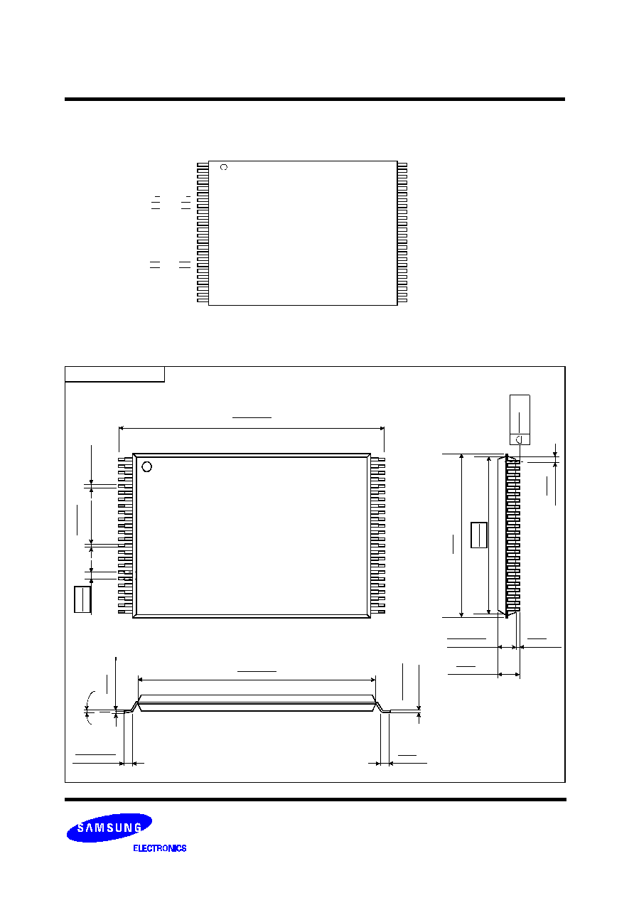
PIN CONFIGURATION (TSOP1)
K9F12XXU0A-YCB0,PCB0/YIB0,PIB0
N.C
N.C
N.C
N.C
N.C
N.C
R/B
RE
CE
N.C
N.C
Vcc
Vss
N.C
N.C
CLE
ALE
WE
WP
N.C
N.C
N.C
N.C
N.C
Vss
I/O15
I/O7
I/O14
I/O6
I/O13
I/O5
I/O12
I/O4
N.C
N.C
Vcc
N.C
N.C
N.C
I/O11
I/O3
I/O10
I/O2
I/O9
I/O1
I/O8
I/O0
Vss
1
2
3
4
5
6
7
8
9
10
11
12
13
14
15
16
17
18
19
20
21
22
23
24
48
47
46
45
44
43
42
41
40
39
38
37
36
35
34
33
32
31
30
29
28
27
26
25
N.C
N.C
N.C
N.C
N.C
N.C
R/B
RE
CE
N.C
N.C
Vcc
Vss
N.C
N.C
CLE
ALE
WE
WP
N.C
N.C
N.C
N.C
N.C
N.C
N.C
N.C
N.C
I/O7
I/O6
I/O5
I/O4
N.C
N.C
N.C
Vcc
Vss
N.C
N.C
N.C
I/O3
I/O2
I/O1
I/O0
N.C
N.C
N.C
N.C
X8
X16
X16
X8
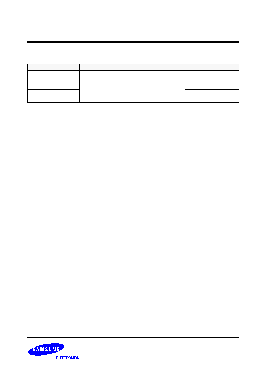
PACKAGE DIMENSIONS
48-PIN LEAD/LEAD FREE PLASTIC THIN SMALL OUT-LINE PACKAGE TYPE(I)
48 - TSOP1 - 1220F
Unit :mm/Inch
0.787
±
0.008
20.00
±
0.20
#1
#24
0
.
1
6
+
0
.
0
7
-
0
.
0
3
0
.
0
0
8
+
0
.
0
0
3
-
0
.
0
0
1
0
.
5
0
0
.
0
1
9
7
#48
#25
0
.
4
8
8
1
2
.
4
0
M
A
X
1
2
.
0
0
0
.
4
7
2
0
.
1
0
0
.
0
0
4
M
A
X
0
.
2
5
0
.
0
1
0
(
)
0.039
±
0.002
1.00
±
0.05
0.002
0.05
MIN
0.047
1.20
MAX
0.45~0.75
0.018~0.030
0.724
±
0.004
18.40
±
0.10
0~8
∞
0
.
0
1
0
0
.
2
5
T
Y
P
0
.
1
2
5
+
0
.
0
7
5
0
.
0
3
5
0
.
0
0
5
+
0
.
0
0
3
-
0
.
0
0
1
0.50
0.020
(
)
0
.
2
0
+
0
.
0
7
-
0
.
0
3
FLASH MEMORY
5
K9F1208D0A
K9F1208U0A
K9F1216D0A
K9F1216U0A
PIN CONFIGURATION (WSOP1)
K9F1208U0A-VCB0,FCB0/VIB0,FIB0
1
2
3
4
5
6
7
8
9
10
11
12
13
14
15
16
17
18
19
20
21
22
23
24
48
47
46
45
44
43
42
41
40
39
38
37
36
35
34
33
32
31
30
29
28
27
26
25
N.C
N.C
DNU
N.C
N.C
N.C
R/B
RE
CE
DNU
N.C
Vcc
Vss
N.C
DNU
CLE
ALE
WE
WP
N.C
N.C
DNU
N.C
N.C
N.C
N.C
DNU
N.C
I/O7
I/O6
I/O5
I/O4
N.C
DNU
N.C
Vcc
Vss
N.C
DNU
N.C
I/O3
I/O2
I/O1
I/O0
N.C
DNU
N.C
N.C
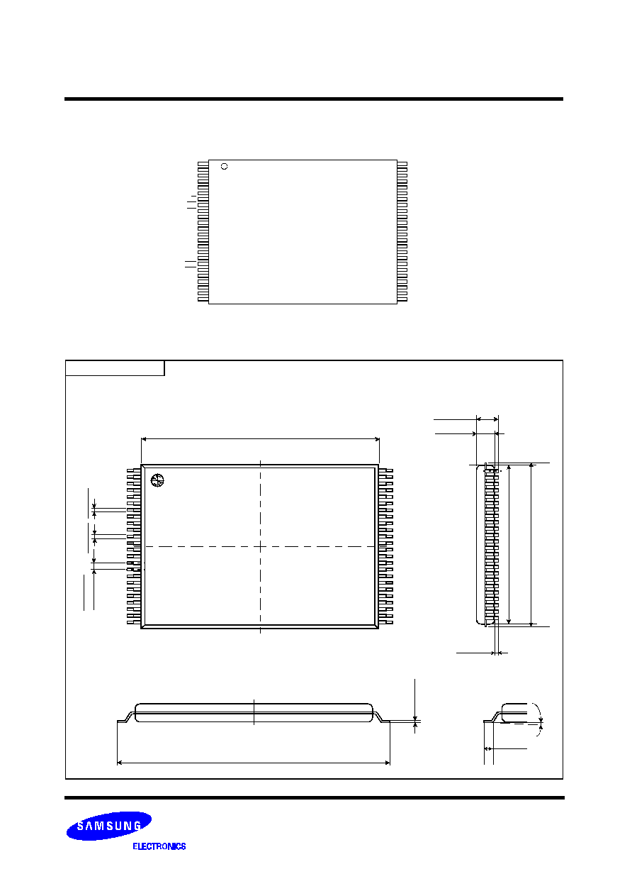
PACKAGE DIMENSIONS
48-PIN LEAD PLASTIC VERY VERY THIN SMALL OUT-LINE PACKAGE TYPE (I)
48 - WSOP1 - 1217F
Unit :mm
15.40
±
0.10
#1
#24
0
.
2
0
+
0
.
0
7
-
0
.
0
3
0
.
1
6
+
0
.
0
7
-
0
.
0
3
0
.
5
0
T
Y
P
(
0
.
5
0
±
0
.
0
6
)
#48
#25
0
.
1
0
+
0
.
0
7
5
-
0
.
0
3
5
17.00
±
0.20
0
∞
~8
∞
0.45~0.75
1
2
.
0
0
±
0
.
1
0
0.58
±
0.04
0.70 MAX
(0.01Min)
1
2
.
4
0
M
A
X