K9F1G08X0A_1.0_final.fm
1
K9F1G08U0A
K9F1G08R0A
K9K2G08U1A
FLASH MEMORY
K9F1G08X0A
* Samsung Electronics reserves the right to change products or specification without notice.
INFORMATION IN THIS DOCUMENT IS PROVIDED IN RELATION TO SAMSUNG PRODUCTS,
AND IS SUBJECT TO CHANGE WITHOUT NOTICE.
NOTHING IN THIS DOCUMENT SHALL BE CONSTRUED AS GRANTING ANY LICENSE,
EXPRESS OR IMPLIED, BY ESTOPPEL OR OTHERWISE,
TO ANY INTELLECTUAL PROPERTY RIGHTS IN SAMSUNG PRODUCTS OR TECHNOLOGY. ALL
INFORMATION IN THIS DOCUMENT IS PROVIDED
ON AS "AS IS" BASIS WITHOUT GUARANTEE OR WARRANTY OF ANY KIND.
1. For updates or additional information about Samsung products, contact your nearest Samsung office.
2. Samsung products are not intended for use in life support, critical care, medical, safety equipment, or similar
applications where Product failure could result in loss of life or personal or physical harm, or any military or
defense application, or any governmental procurement to which special terms or provisions may apply.
2
K9F1G08U0A
K9F1G08R0A
K9K2G08U1A
FLASH MEMORY
Document Title
128M x 8 Bit / 256M x 8 Bit
NAND Flash Memory
Revision History
The attached data sheets are prepared and approved by SAMSUNG Electronics. SAMSUNG Electronics CO., LTD. reserve the right
to change the specifications. SAMSUNG Electronics will evaluate and reply to your requests and questions about device. If you have
any questions, please contact the SAMSUNG branch office near your office.
Revision No
0.0
0.1
0.2
0.3
0.4
0.5
0.6
0.7
0.8
1.0
Remark
Advance
Preliminary
Preliminary
Preliminary
Preliminary
Preliminary
History
1. Initial issue
1. The tADL(Address to Data Loading Time) is added.
- tADL Minimum 100ns (Page 11, 23~26)
-
tADL is the time from the WE rising edge of final address cycle
to the WE rising edge of first data cycle at program operation.
2. Added Addressing method for program operation
1. Add the Protrusion/Burr value in WSOP1 PKG Diagram.
1. PKG(TSOP1, WSOP1) Dimension Change
1. Technical note is changed
2. Notes of AC timing characteristics are added
3. The description of Copy-back program is changed
4. Voltage range is changed
-1.7V~1.95V -> 1.65V~1.95V
5. Note2 of Command Sets is added
1. CE access time : 23ns->35ns (p.11)
1. The value of tREA for 3.3V device is changed.(18ns->20ns)
2. EDO mode is added.
1. The flow chart to creat the initial invalid block table is cahnged.
1. 1.8V FBGA package is added
1. 3.3V FBGA package is added
Draft Date
Aug. 24. 2003
Jan. 27. 2004
Apr. 23. 2004
May. 19. 2004
Jan. 21. 2005
Feb. 14. 2005
May. 4. 2005
May 6. 2005
Aug. 5. 2005
Jan. 27. 2006
3
K9F1G08U0A
K9F1G08R0A
K9K2G08U1A
FLASH MEMORY
GENERAL DESCRIPTION
FEATURES
· Voltage Supply
-1.8V device(K9F1G08R0A): 1.65V~1.95V
-3.3V device(K9F1G08U0A): 2.7 V ~3.6 V
· Organization
- Memory Cell Array : (128M + 4,096K)bit x 8bit
- Data Register : (2K + 64)bit x8bit
- Cache Register : (2K + 64)bit x8bit
· Automatic Program and Erase
- Page Program : (2K + 64)Byte
- Block Erase : (128K + 4K)Byte
· Page Read Operation
- Page Size : 2K-Byte
- Random Read : 25
µs(Max.)
- Serial Access : 30ns(Min.) - 3.3v device
50ns(Min.) -1.8v device
128M x 8 Bit /256M x 8 Bit NAND Flash Memory
· Fast Write Cycle Time
- Program time : 200
µs(Typ.)
- Block Erase Time : 2ms(Typ.)
· Command/Address/Data Multiplexed I/O Port
· Hardware Data Protection
- Program/Erase Lockout During Power Transitions
· Reliable CMOS Floating-Gate Technology
- Endurance : 100K Program/Erase Cycles
- Data Retention : 10 Years
· Command Register Operation
· Cache Program Operation for High Performance Program
· Intelligent Copy-Back Operation
· Unique ID for Copyright Protection
· Package :
- K9F1G08X0A-JCB0/JIB0
63- Ball FBGA (9.5 x 12) - Pb-free Package
- K9F1G08U0A-PCB0/PIB0
48 - Pin TSOP I (12 x 20 / 0.5 mm pitch)- Pb-free Package
- K9F1G08U0A-FIB0
48 - Pin WSOP I (12X17X0.7mm)- Pb-free Package
* K9F1G08U0A-F(WSOPI ) is the same device as
K9F1G08U0A-P(TSOP1) except package type.
- K9K2G08U1A-ICB0/IIB0
52-ULGA (12X17X0.65mm)
Offered in 128Mx8bit the K9F1G08X0A is 1G bit with spare 32M bit capacity. Its NAND cell provides the most cost-effective solution
for the solid state mass storage market. A program operation can be performed in typical 200
µs on the 2112-byte page and an erase
operation can be performed in typical 2ms on a 128K-byte block. Data in the data page can be read out at 30ns(50ns with 1.8V
device) cycle time per byte. The I/O pins serve as the ports for address and data input/output as well as command input. The on-chip
write controller automates all program and erase functions including pulse repetition, where required, and internal verification and
margining of data. Even the write-intensive systems can take advantage of the K9F1G08X0A
s extended reliability of 100K program/
erase cycles by providing ECC(Error Correcting Code) with real time mapping-out algorithm. The K9F1G08X0A is an optimum solu-
tion for large nonvolatile storage applications such as solid state file storage and other portable applications requiring non-volatility.
PRODUCT LIST
Part Number
Vcc Range
Organization
PKG Type
K9F1G08R0A-J
1.65 ~ 1.95V
X8
FBGA
K9F1G08U0A-P
2.7 ~ 3.6V
TSOP1
K9F1G08U0A-F
WSOP1
K9F1G08U0A-J
FBGA
K9K2G08U1A-I
52-ULGA
4
K9F1G08U0A
K9F1G08R0A
K9K2G08U1A
FLASH MEMORY
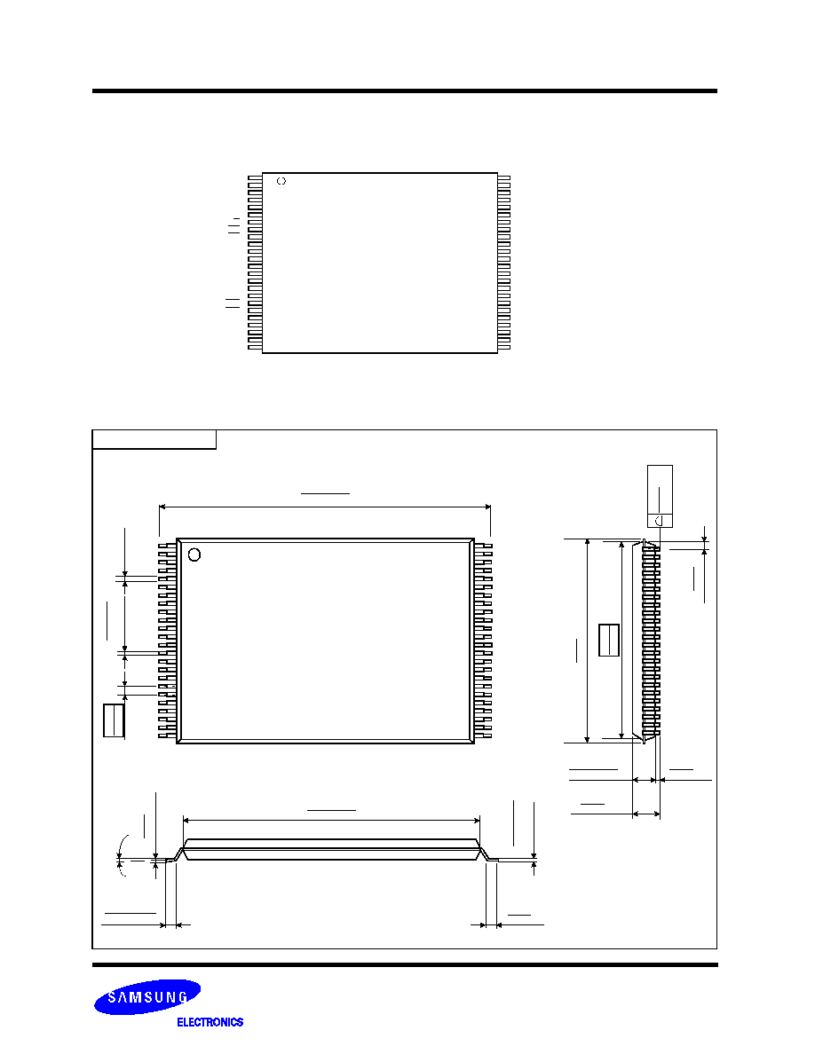
PIN CONFIGURATION (TSOP1)
K9F1G08U0A-PCB0/PIB0
PACKAGE DIMENSIONS
48-PIN LEAD/LEAD FREE PLASTIC THIN SMALL OUT-LINE PACKAGE TYPE(I)
48 - TSOP1 - 1220AF
Unit :mm/Inch
0.787
±0.008
20.00
±0.20
#1
#24
0.1
6
+0.
0
7
-0
.
0
3
0.
00
8
+0.
003
-
0
.001
0.
50
0.
0197
#48
#25
0.
488
12
.40
MAX
12
.00
0.
472
0.1
0
0.
004
MAX
0.2
5
0.
010
()
0.039
±0.002
1.00
±0.05
0.002
0.05
MIN
0.047
1.20
MAX
0.45~0.75
0.018~0.030
0.724
±0.004
18.40
±0.10
0~8
°
0.
010
0.2
5
TYP
0.
125
+0
.
0
75
0.0
3
5
0.
00
5
+0
.
0
0
3
-0
.0
0
1
0.50
0.020
(
)
48-pin TSOP1
Standard Type
12mm x 20mm
1
2
3
4
5
6
7
8
9
10
11
12
13
14
15
16
17
18
19
20
21
22
23
24
48
47
46
45
44
43
42
41
40
39
38
37
36
35
34
33
32
31
30
29
28
27
26
25
N.C
N.C
N.C
N.C
N.C
N.C
R/B
RE
CE
N.C
N.C
Vcc
Vss
N.C
N.C
CLE
ALE
WE
WP
N.C
N.C
N.C
N.C
N.C
N.C
N.C
N.C
N.C
I/O7
I/O6
I/O5
I/O4
N.C
N.C
N.C
Vcc
Vss
N.C
N.C
N.C
I/O3
I/O2
I/O1
I/O0
N.C
N.C
N.C
N.C
0.
20
+0.
0
7
-0
.
0
3
5
K9F1G08U0A
K9F1G08R0A
K9K2G08U1A
FLASH MEMORY
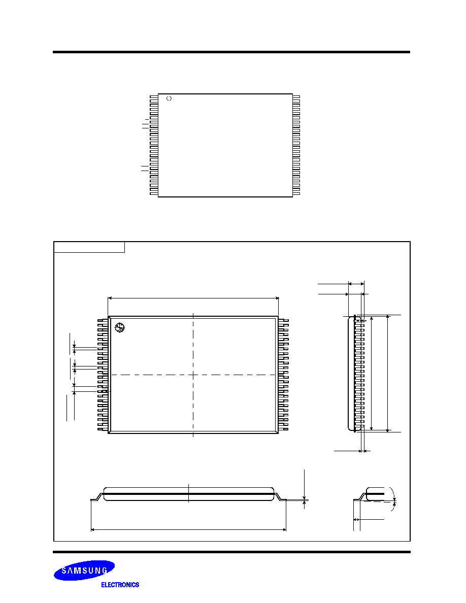
PIN CONFIGURATION (WSOP1)
K9F1G08U0A-FIB0
1
2
3
4
5
6
7
8
9
10
11
12
13
14
15
16
17
18
19
20
21
22
23
24
48
47
46
45
44
43
42
41
40
39
38
37
36
35
34
33
32
31
30
29
28
27
26
25
N.C
N.C
DNU
N.C
N.C
N.C
R/B
RE
CE
DNU
N.C
Vcc
Vss
N.C
DNU
CLE
ALE
WE
WP
N.C
N.C
DNU
N.C
N.C
N.C
N.C
DNU
N.C
I/O7
I/O6
I/O5
I/O4
N.C
DNU
N.C
Vcc
Vss
N.C
DNU
N.C
I/O3
I/O2
I/O1
I/O0
N.C
DNU
N.C
N.C
PACKAGE DIMENSIONS
48-PIN LEAD PLASTIC VERY VERY THIN SMALL OUT-LINE PACKAGE TYPE (I)
48 - WSOP1 - 1217F
Unit :mm
15.40
±0.10
#1
#24
0.2
0
+0
.
0
7
-0
.0
3
0.
16
+0
.
0
7
-0
.0
3
0.
5
0
T
Y
P
(0.
5
0
±
0.
06)
#48
#25
0.
10
+
0
.075
-0
.0
3
5
17.00
±0.20
0°
~8
°
0.45~0.75
12
.0
0
±
0.10
0.58
±0.04
0.70 MAX
(0.01Min)
12.
40MA
X