
FLASH MEMORY
1
Advance
K9F4G08U0M
K9K8G08U1M
Document Title
512M x 8 Bits / 1G x 8 Bits NAND Flash Memory
Revision History
The attached data sheets are prepared and approved by SAMSUNG Electronics. SAMSUNG Electronics CO., LTD. reserve the right
to change the specifications. SAMSUNG Electronics will evaluate and reply to your requests and questions about device. If you have
any questions, please contact the SAMSUNG branch office near your office.
Revision No
0.0
Remark
Advance
History
1. Initial issue
Draft Date
Nov. 15. 2004
FLASH MEMORY
2
Advance
K9F4G08U0M
K9K8G08U1M
GENERAL DESCRIPTION
FEATURES
∑ Voltage Supply
- 2.70V ~ 3.60V
∑ Organization
- Memory Cell Array : (512M + 16,384K)bit x 8bit
- Data Register : (2K + 64)bit x 8bit
∑ Automatic Program and Erase
- Page Program : (2K + 64)Byte
- Block Erase : (128K + 4K)Byte
∑ Page Read Operation
- Page Size : (2K + 64)Byte
- Random Read : 20
µs(Max.)
- Serial Access : 25ns(Min.)
512M x 8 Bit / 1G x 8 Bits NAND Flash Memory
∑ Fast Write Cycle Time
- Page Program time : 200
µs(Typ.)
- Block Erase Time : 1.5ms(Typ.)
∑ Command/Address/Data Multiplexed I/O Port
∑ Hardware Data Protection
- Program/Erase Lockout During Power Transitions
∑ Reliable CMOS Floating-Gate Technology
- Endurance : 100K Program/Erase Cycles
- Data Retention : 10 Years
∑ Command Driven Operation
∑ Intelligent Copy-Back with internal 1bit/528Byte EDC
∑ Unique ID for Copyright Protection
∑ Package :
- K9F4G08U0M-YCB0/YIB0
48 - Pin TSOP I (12 x 20 / 0.5 mm pitch)
- K9F4G08U0M-PCB0/PIB0 : Pb-FREE PACKAGE
48 - Pin TSOP I (12 x 20 / 0.5 mm pitch)
- K9F4G08U0M-ICB0/IIB0
52 - Pin ULGA (12 x 17 / 1.00 mm pitch)
- K9K8G08U1M-ICB0/IIB0
52 - Pin ULGA (12 x 17 / 1.00 mm pitch)
Offered in 512Mx8bit, the K9F4G08U0M is a 4G-bit NAND Flash Memory with spare 128M-bit. Its NAND cell provides the most cost-
effective solution for the solid state application market. A program operation can be performed in typical 200
µs on the (2K+64)Byte
page and an erase operation can be performed in typical 1.5ms on a (128K+4K)Byte block. Data in the data page can be read out at
25ns cycle time per Byte. The I/O pins serve as the ports for address and data input/output as well as command input. The on-chip
write controller automates all program and erase functions including pulse repetition, where required, and internal verification and
margining of data. Even the write-intensive systems can take advantage of the K9F4G08U0M
s extended reliability of 100K program/
erase cycles by providing ECC(Error Correcting Code) with real time mapping-out algorithm. The K9F4G08U0M is an optimum solu-
tion for large nonvolatile storage applications such as solid state file storage and other portable applications requiring non-volatility.
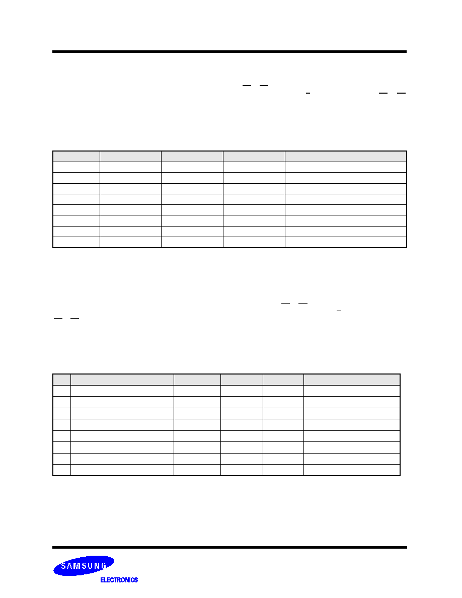
PRODUCT LIST
Part Number
Vcc Range
Organization
PKG Type
K9F4G08U0M-Y,P
2.70 ~ 3.60V
X8
TSOP1
K9F4G08U0M-I
52ULGA
K9K8G08U1M-I
FLASH MEMORY
3
Advance
K9F4G08U0M
K9K8G08U1M
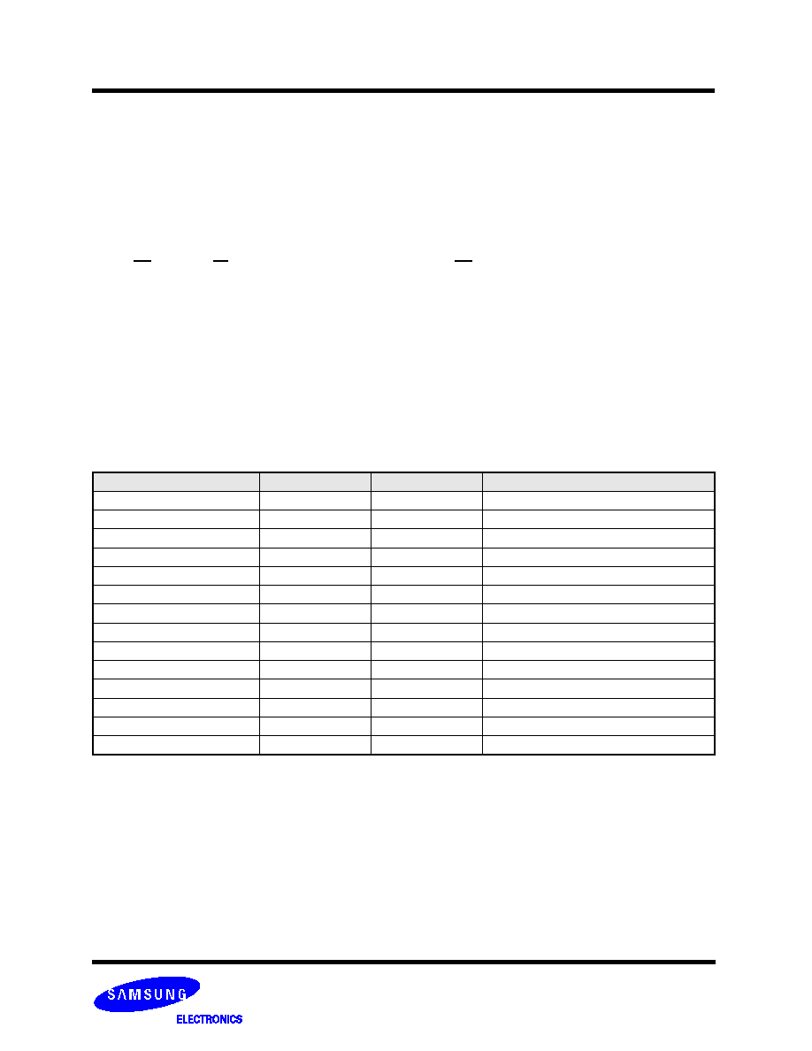
PIN CONFIGURATION (TSOP1)
K9F4G08U0M-YCB0,PCB0/YIB0,PIB0
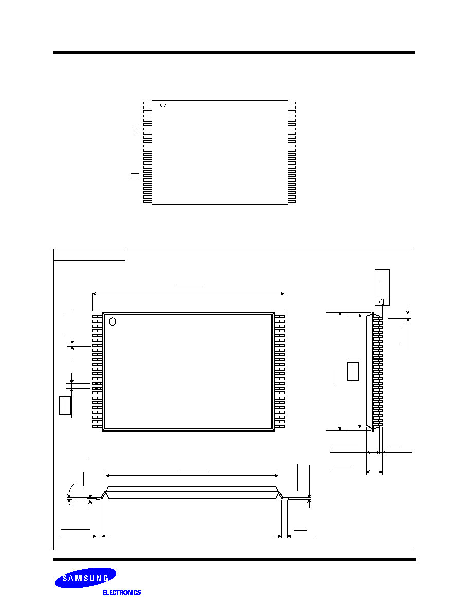
PACKAGE DIMENSIONS
48-PIN LEAD/LEAD FREE PLASTIC THIN SMALL OUT-LINE PACKAGE TYPE(I)
48 - TSOP1 - 1220F
Unit :mm/Inch
0.787
±0.008
20.00
±0.20
#1
#24
0.
20
+0
.
0
7
-0
.0
3
0.
008
+
0
.003
-0
.0
0
1
0.
50
0.
019
7
#48
#25
0.
488
12
.40
MAX
12
.00
0.
472
0.1
0
0.
004
MAX
0.2
5
0.
010
()
0.039
±0.002
1.00
±0.05
0.002
0.05
MIN
0.047
1.20
MAX
0.45~0.75
0.018~0.030
0.724
±0.004
18.40
±0.10
0~8
∞
0.
010
0.2
5
TYP
0.
125
+0
.
0
75
0.0
3
5
0.
00
5
+0
.
0
0
3
-0
.0
0
1
0.50
0.020
(
)
48-pin TSOP1
Standard Type
12mm x 20mm
1
2
3
4
5
6
7
8
9
10
11
12
13
14
15
16
17
18
19
20
21
22
23
24
48
47
46
45
44
43
42
41
40
39
38
37
36
35
34
33
32
31
30
29
28
27
26
25
N.C
N.C
N.C
N.C
N.C
N.C
R/B
RE
CE
N.C
N.C
Vcc
Vss
N.C
N.C
CLE
ALE
WE
WP
N.C
N.C
N.C
N.C
N.C
N.C
N.C
N.C
N.C
I/O7
I/O6
I/O5
I/O4
N.C
N.C
N.C
Vcc
Vss
N.C
N.C
N.C
I/O3
I/O2
I/O1
I/O0
N.C
N.C
N.C
N.C
FLASH MEMORY
4
Advance
K9F4G08U0M
K9K8G08U1M
1.00
1.00
1.00
1.00
2.00
7 6 5 4 3 2 1
1.
00
1.0
0
1.0
0
12.00
±0.10
#A1
17.
00
±
0.
10
17
.00
±
0.1
0
B
A
12.00
±0.10
(Datum B)
(Datum A)
12.
0
0
10.00
2.
50
2.
50
2.
00
0.5
0
1.
30
A
B
C
D
E
F
G
H
J
K
L
M
N
12-
1.00±0.05
41-
0.70
±
0.05
Side View
0.
65
(
Max
.)
0.10 C
17.00
±0.10
Top View
Bottom View
A
B
C
D E
F
G
H J
K
L
M
N
7
6
5
4
3
2
1
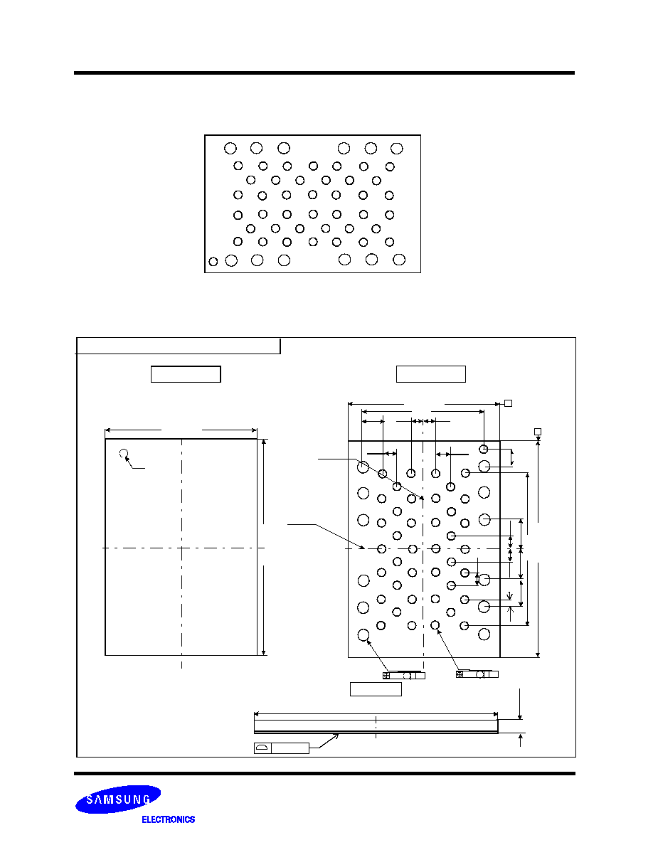
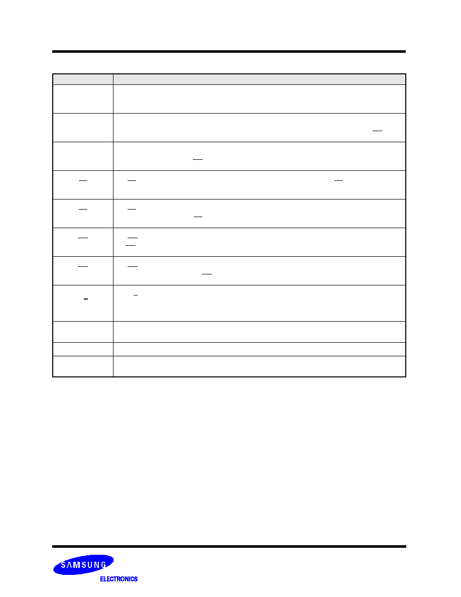
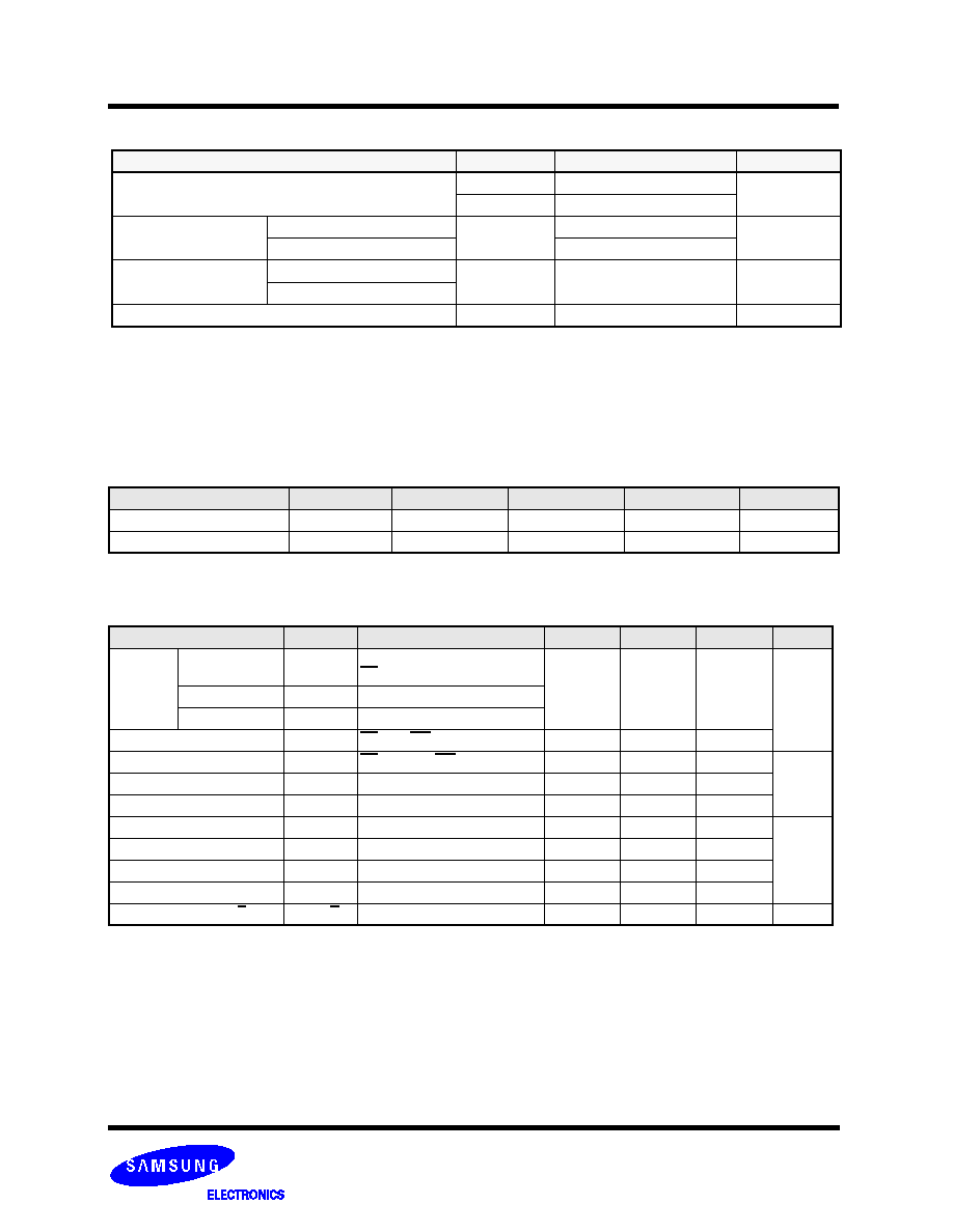
PIN CONFIGURATION (ULGA)
K9F4G08U0M-ICB0/IIB0
52-ULGA (measured in millimeters)
NC
NC
NC
NC
NC
NC
NC
NC
NC
NC
NC
NC
NC
NC
NC
NC
Vcc
Vcc
Vss
Vss
Vss
/RE
NC
/CE
NC
CLE
NC
ALE
NC
/WE
NC
/WP
NC
R/B
NC
Vss
IO0
NC
IO1
NC
IO2
IO3
NC
NC
IO4
NC
IO5
NC
IO6
NC
IO7
NC
AB
C
M
0.1
AB
C
M
0.1
PACKAGE DIMENSIONS

FLASH MEMORY
5
Advance
K9F4G08U0M
K9K8G08U1M
1.00
1.00
1.00
1.00
2.00
7 6 5 4 3 2 1
1.
00
1.0
0
1.0
0
12.00
±0.10
#A1
17.
00
±
0.
10
17
.00
±
0.1
0
B
A
12.00
±0.10
(Datum B)
(Datum A)
12.
0
0
10.00
2.
50
2.
50
2.
00
0.5
0
1.
30
A
B
C
D
E
F
G
H
J
K
L
M
N
12-
1.00±0.05
41-
0.70
±
0.05
Side View
0.
65
(
Max
.)
0.10 C
17.00
±0.10
Top View
Bottom View
A
B
C
D E
F
G
H J
K
L
M
N
7
6
5
4
3
2
1
K9K8G08U1M-ICB0/IIB0
52-ULGA (measured in millimeters)
NC
NC
NC
NC
NC
NC
NC
NC
NC
NC
NC
NC
NC
NC
NC
NC
Vcc
Vcc
Vss
Vss
Vss
/RE1
/RE2
/CE1
/CE2
CLE1
CLE2
ALE1
ALE2
/WE1
/WE2
/WP1
/WP2
R/B1
R/B2
Vss
IO0-1
IO0-2
IO1-1
IO1-2
IO2-1
IO3-1
IO2-2
IO3-2
IO4-1
IO4-2
IO5-1
IO5-2
IO6-1
IO6-2
IO7-1
IO7-2
AB
C
M
0.1
AB
C
M
0.1
PACKAGE DIMENSIONS
FLASH MEMORY
6
Advance
K9F4G08U0M
K9K8G08U1M
PIN DESCRIPTION
NOTE : Connect all V
CC
and V
SS
pins of each device to common power supply outputs.
Do not leave V
CC
or V
SS
disconnected.
Pin Name
Pin Function
I/O
0
~ I/O
7
DATA INPUTS/OUTPUTS
The I/O pins are used to input command, address and data, and to output data during read operations. The I/
O pins float to high-z when the chip is deselected or when the outputs are disabled.
CLE
COMMAND LATCH ENABLE
The CLE input controls the activating path for commands sent to the command register. When active high,
commands are latched into the command register through the I/O ports on the rising edge of the WE signal.
ALE
ADDRESS LATCH ENABLE
The ALE input controls the activating path for address to the internal address registers. Addresses are
latched on the rising edge of WE with ALE high.
CE
CHIP ENABLE
The CE input is the device selection control. When the device is in the Busy state, CE high is ignored, and
the device does not return to standby mode in program or erase operation.
RE
READ ENABLE
The RE input is the serial data-out control, and when active drives the data onto the I/O bus. Data is valid
tREA after the falling edge of RE which also increments the internal column address counter by one.
WE
WRITE ENABLE
The WE input controls writes to the I/O port. Commands, address and data are latched on the rising edge of
the WE pulse.
WP
WRITE PROTECT
The WP pin provides inadvertent program/erase protection during power transitions. The internal high volt-
age generator is reset when the WP pin is active low.
R/B
READY/BUSY OUTPUT
The R/B output indicates the status of the device operation. When low, it indicates that a program, erase or
random read operation is in process and returns to high state upon completion. It is an open drain output and
does not float to high-z condition when the chip is deselected or when outputs are disabled.
Vcc
POWER
V
CC
is the power supply for device.
Vss
GROUND
N.C
NO CONNECTION
Lead is not internally connected.
FLASH MEMORY
7
Advance
K9F4G08U0M
K9K8G08U1M
2K Bytes
64 Bytes
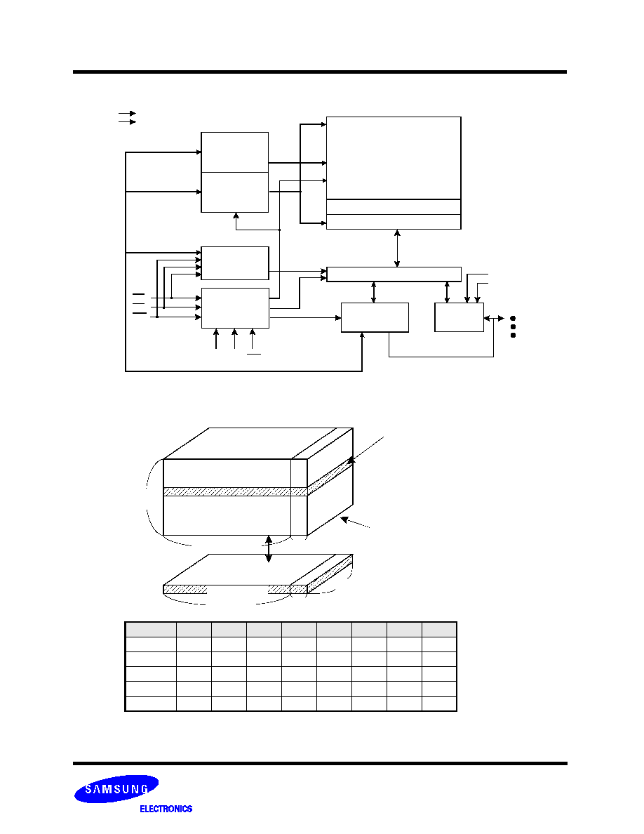
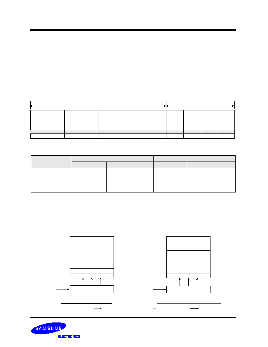
Figure 1. K9F4G08U0M Functional Block Diagram
Figure 2. K9F4G08U0M Array Organization
NOTE : Column Address : Starting Address of the Register.
* L must be set to "Low".
* The device ignores any additional input of address cycles than reguired.
I/O 0
I/O 1
I/O 2
I/O 3
I/O 4
I/O 5
I/O 6
I/O 7
1st Cycle
A
0
A
1
A
2
A
3
A
4
A
5
A
6
A
7
2nd Cycle
A
8
A
9
A
10
A
11
*L
*L
*L
*L
3rd Cycle
A
12
A
13
A
14
A
15
A
16
A
17
A
18
A
19
4th Cycle
A
20
A
21
A
22
A
23
A
24
A
25
A
26
A
27
5th Cycle
A
28
A
29
*L
*L
*L
*L
*L
*L
V
CC
X-Buffers
Command
I/O Buffers & Latches
Latches
& Decoders
Y-Buffers
Latches
& Decoders
Register
Control Logic
& High Voltage
Generator
Global Buffers
Output
Driver
V
SS
A
12
- A
29
A
0
- A
11
Command
CE
RE
WE
CLE
WP
I/0 0
I/0 7
V
CC
V
SS
256K Pages
(=4,096 Blocks)
2K Bytes
8 bit
64 Bytes
1 Block = 64 Pages
(128K + 4k) Byte
I/O 0 ~ I/O 7
1 Page = (2K + 64)Bytes
1 Block = (2K + 64)B x 64 Pages
= (128K + 4K) Bytes
1 Device = (2K+64)B x 64Pages x 4,096 Blocks
= 4,224 Mbits
Row Address
Page Register
ALE
4,096M + 128M Bit
NAND Flash
ARRAY
(2,048 + 64)Byte x 262,144
Y-Gating
Row Address
Column Address
Column Address
Row Address
Data Register & S/A
FLASH MEMORY
8
Advance
K9F4G08U0M
K9K8G08U1M
Product Introduction
The K9F4G08U0M is a 4,224Mbit(4,429,185,024 bit) memory organized as 262,144 rows(pages) by 2,112x8 columns. Spare 64x8
columns are located from column address of 2,048~2,111. A 2,112-byte data register is connected to memory cell arrays accommo-
dating data transfer between the I/O buffers and memory during page read and page program operations. The memory array is made
up of 32 cells that are serially connected to form a NAND structure. Each of the 32 cells resides in a different page. A block consists
of two NAND structured strings. A NAND structure consists of 32 cells. Total 1,081,344 NAND cells reside in a block. The program
and read operations are executed on a page basis, while the erase operation is executed on a block basis. The memory array con-
sists of 4,096 separately erasable 128K-byte blocks. It indicates that the bit by bit erase operation is prohibited on the K9F4G08U0M.
The K9F4G08U0M has addresses multiplexed into 8 I/Os. This scheme dramatically reduces pin counts and allows system upgrades
to future densities by maintaining consistency in system board design. Command, address and data are all written through I/O's by
bringing WE to low while CE is low. Those are latched on the rising edge of WE. Command Latch Enable(CLE) and Address Latch
Enable(ALE) are used to multiplex command and address respectively, via the I/O pins. Some commands require one bus cycle. For
example, Reset Command, Status Read Command, etc require just one cycle bus. Some other commands, like page read and block
erase and page program, require two cycles: one cycle for setup and the other cycle for execution. The 528M byte physical space
requires 30 addresses, thereby requiring five cycles for addressing : 2 cycles of column address, 3 cycles of row address, in that
order. Page Read and Page Program need the same five address cycles following the required command input. In Block Erase oper-
ation, however, only the three row address cycles are used. Device operations are selected by writing specific commands into the
command register. Table 1 defines the specific commands of the K9F4G08U0M.
In addition to the enhanced architecture and interface, the device incorporates copy-back program feature from one page to another
page without need for transporting the data to and from the external buffer memory. Since the time-consuming serial access and
data-input cycles are removed, system performance for solid-state disk application is significantly increased.
Table 1. Command Sets
NOTE : 1. Random Data Input/Output can be executed in a page.
2. Read EDC Status is only available on Copy Back operation.
Caution :
Any undefined command inputs are prohibited except for above command set of Table 1.
Function
1st. Cycle
2nd. Cycle
Acceptable Command during Busy
Read 00h
30h
Read for Copy Back
00h
35h
Read ID
90h
-
Reset
FFh
-
O
Page Program
80h
10h
Two-Plane Page Program
80h---11h
81h---10h
Copy-Back Program
85h
10h
Two-Plane Copy-Back Program
85h---11h
81h---10h
Block Erase
60h
D0h
Two-Plane Block Erase
60h---60h
D0h
Random Data Input
(1)
85h
-
Random Data Output
(1)
05h
E0h
Read Status
70h
O
Read EDC Status
(2)
7Bh
O
FLASH MEMORY
9
Advance
K9F4G08U0M
K9K8G08U1M
DC AND OPERATING CHARACTERISTICS
(Recommended operating conditions otherwise noted.)
NOTE : 1. V
IL
can undershoot to -0.4V and V
IH
can overshoot to V
CC
+0.4V for durations of 20 ns or less.
2. Typical value is measured at Vcc=3.3V, T
A
=25
∞C. Not 100% tested.
Parameter
Symbol
Test Conditions
Min
Typ
Max
Unit
Operating
Current
Page Read with
Serial Access
I
CC
1
tRC=25ns
CE=V
IL,
I
OUT
=0mA
-
15
30
mA
Program
I
CC
2
-
Erase
I
CC
3
-
Stand-by Current(TTL)
I
SB
1
CE=V
IH
, WP=0V/V
CC
-
-
1
Stand-by Current(CMOS)
I
SB
2
CE=V
CC
-0.2, WP=0V/V
CC
-
10
50
µA
Input Leakage Current
I
LI
V
IN
=0 to Vcc(max)
-
-
±10
Output Leakage Current
I
LO
V
OUT
=0 to Vcc(max)
-
-
±10
Input High Voltage
V
IH*
-
0.8xVcc
-
Vcc+0.3
V
Input Low Voltage, All inputs
V
IL*
-
-0.3
-
0.2xVcc
Output High Voltage Level
V
OH
K9F4G08U0M :I
OH
=-400
µA
2.4
-
-
Output Low Voltage Level
V
OL
K9F4G08U0M :I
OL
=2.1mA
-
-
0.4
Output Low Current(R/B)
I
OL
(R/B)
K9F4G08U0M :V
OL
=0.4V
8
10
-
mA
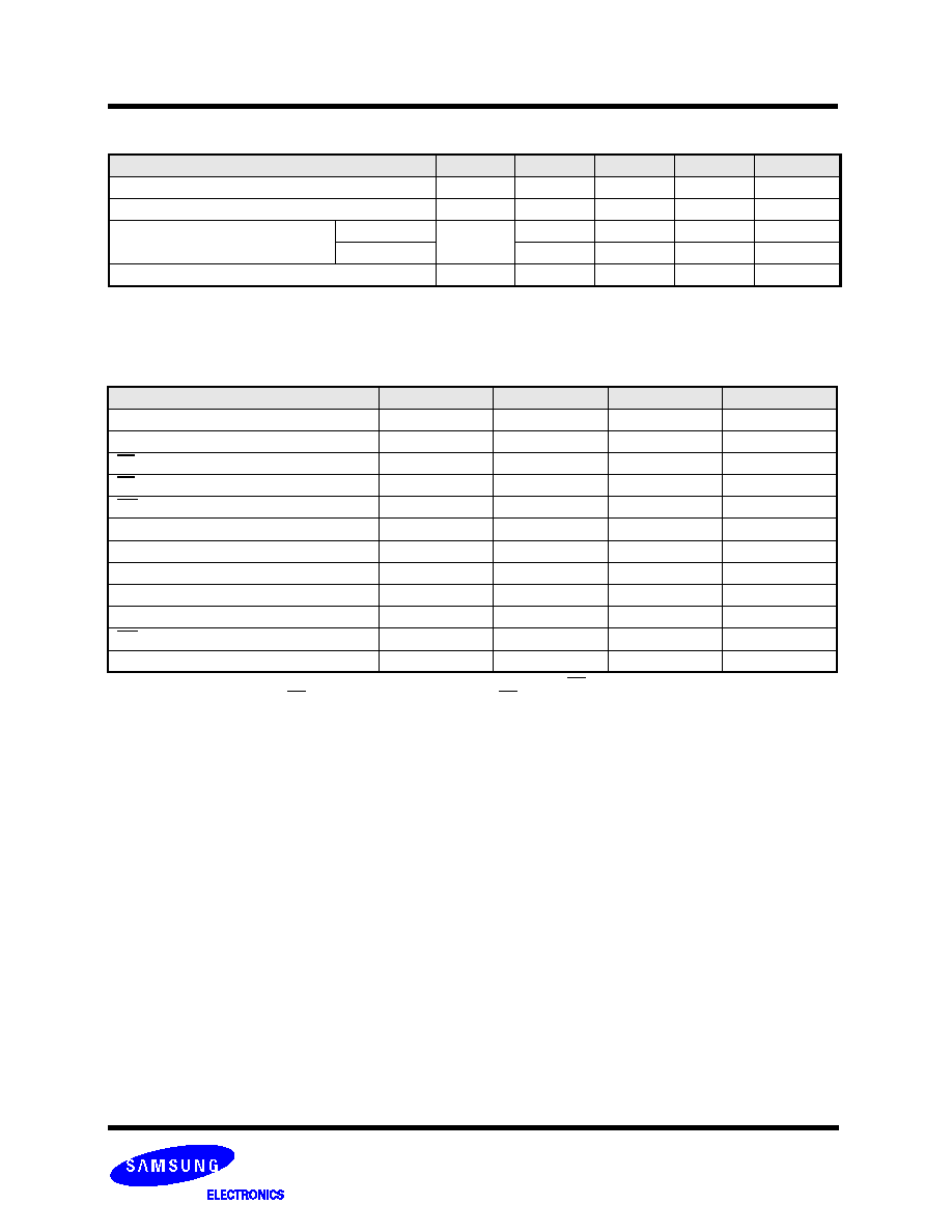
RECOMMENDED OPERATING CONDITIONS
(Voltage reference to GND, K9F4G08U0M-XCB0
:
T
A
=0 to 70
∞C, K9F4G08U0M-XIB0
:
T
A
=-40 to 85
∞C)
Parameter
Symbol
Min
Typ.
Max
Unit
Supply Voltage
V
CC
2.7
3.3
3.6
V
Supply Voltage
V
SS
0
0
0
V
ABSOLUTE MAXIMUM RATINGS
NOTE :
1. Minimum DC voltage is -0.6V on input/output pins. During transitions, this level may undershoot to -2.0V for periods <30ns.
Maximum DC voltage on input/output pins is V
CC
+0.3V which, during transitions, may overshoot to V
CC
+2.0V for periods <20ns.
2. Permanent device damage may occur if ABSOLUTE MAXIMUM RATINGS are exceeded. Functional operation should be restricted to the conditions
as detailed in the operational sections of this data sheet. Exposure to absolute maximum rating conditions for extended periods may affect reliability.
Parameter
Symbol
Rating
Unit
Voltage on any pin relative to VSS
V
IN/OUT
-0.6 to +4.6
V
V
CC/
V
CCQ
-0.6 to +4.6
Temperature Under Bias
K9F4G08U0M-XCB0
T
BIAS
-10 to +125
∞C
K9F4G08U0M-XIB0
-40 to +125
Storage Temperature
K9F4G08U0M-XCB0
T
STG
-65 to +150
∞C
K9F4G08U0M-XIB0
Short Circuit Current
I
OS
5
mA
FLASH MEMORY
10
Advance
K9F4G08U0M
K9K8G08U1M
CAPACITANCE
(
T
A
=25
∞C, V
CC
=3.3V, f=1.0MHz)
NOTE : Capacitance is periodically sampled and not 100% tested.
Item
Symbol
Test Condition
Min
Max
Unit
Input/Output Capacitance
C
I/O
V
IL
=0V
-
10
pF
Input Capacitance
C
IN
V
IN
=0V
-
10
pF
VALID BLOCK
NOTE :
1. The device may include invalid blocks when first shipped. Additional invalid blocks may develop while being used. The number of valid blocks is pre-
sented with both cases of invalid blocks considered. Invalid blocks are defined as blocks that contain one or more bad bits. Do not erase or program
factory-marked bad blocks. Refer to the attached technical notes for appropriate management of invalid blocks.
2. The 1st block, which is placed on 00h block address, is guaranteed to be a valid block, does not require Error Correction up to 1K program/erase
cycles.
* : Each K9F4G08U0M chip in the K9K8G08U1M has Maximun 80 invalid block.
Parameter
Symbol
Min
Typ.
Max
Unit
K9F4G08U0M
N
VB
4,016
-
4,096
Blocks
K9K8G08U1M
N
VB
8,032*
-
8,192*
Blocks
AC TEST CONDITION
(K9F4G08U0M-XCB0 :T
A
=0 to 70
∞C, K9F4G08U0M-XIB0:T
A
=-40 to 85
∞C
K9F4G08U0M : Vcc=2.7V~3.6V unless otherwise noted)
Parameter
K9F4G08U0M
Input Pulse Levels
0V to Vcc
Input Rise and Fall Times
5ns
Input and Output Timing Levels
Vcc/2
Output Load
1 TTL GATE and CL=50pF
MODE SELECTION
NOTE : 1. X can be V
IL
or V
IH.
2. WP should be biased to CMOS high or CMOS low for standby.
CLE
ALE
CE
WE
RE
WP
Mode
H
L
L
H
X
Read Mode
Command Input
L
H
L
H
X
Address Input(5clock)
H
L
L
H
H
Write Mode
Command Input
L
H
L
H
H
Address Input(5clock)
L
L
L
H
H
Data Input
L
L
L
H
X
Data Output
X
X
X
X
H
X
During Read(Busy)
X
X
X
X
X
H
During Program(Busy)
X
X
X
X
X
H
During Erase(Busy)
X
X
(1)
X
X
X
L
Write Protect
X
X
H
X
X
0V/V
CC
(2)
Stand-by
FLASH MEMORY
11
Advance
K9F4G08U0M
K9K8G08U1M
AC Timing Characteristics for Command / Address / Data Input
NOTES : 1. The transition of the corresponding control pins must occur only once while WE is held low
2. tADL is the time from the WE rising edge of final address cycle to the WE rising edge of first data cycle
Parameter
Symbol
Min
Max
Unit
CLE Setup Time
t
CLS
(1)
12
-
ns
CLE Hold Time
t
CLH
5
-
ns
CE Setup Time
t
CS
(1)
20
-
ns
CE Hold Time
t
CH
5
-
ns
WE Pulse Width
t
WP
12
-
ns
ALE Setup Time
t
ALS
(1)
12
-
ns
ALE Hold Time
t
ALH
5
-
ns
Data Setup Time
t
DS
(1)
12
-
ns
Data Hold Time
t
DH
5
-
ns
Write Cycle Time
t
WC
25
-
ns
WE High Hold Time
t
WH
10
-
ns
ALE to Data Loading Time
t
ADL
(2)
70
-
ns
Program / Erase Characteristics
NOTE : 1. Typical value is measured at Vcc=3.3V, T
A
=25
∞C. Not 100% tested.
2. Typical program time is defined as the time that more than 50% of the whole pages are programmed at Vcc of 3.3V and temperature of 25
∞C
within.
Parameter
Symbol
Min
Typ
Max
Unit
Program Time
t
PROG
(2)
-
200
700
µs
Dummy Busy Time for Two-Plane Page Program
t
DBSY
-
0.5
1
µs
Number of Partial Program Cycles
in the Same Page
Main Array
Nop
-
-
4
cycles
Spare Array
-
-
4
cycles
Block Erase Time
t
BERS
-
1.5
2
ms

FLASH MEMORY
12
Advance
K9F4G08U0M
K9K8G08U1M
AC Characteristics for Operation
NOTE: 1. If reset command(FFh) is written at Ready state, the device goes into Busy for maximum 5us.
Parameter
Symbol
Min
Max
Unit
Data Transfer from Cell to Register
t
R
-
20
µs
ALE to RE Delay
t
AR
10
-
ns
CLE to RE Delay
t
CLR
10
-
ns
Ready to RE Low
t
RR
20
-
ns
RE Pulse Width
t
RP
12
-
ns
WE High to Busy
t
WB
-
100
ns
Read Cycle Time
t
RC
25
-
ns
RE Access Time
t
REA
-
18
ns
CE Access Time
t
CEA
-
23
ns
RE High to Output Hi-Z
t
RHZ
-
100
ns
CE High to Output Hi-Z
t
CHZ
-
30
ns
RE High to Output Hold
t
RHOH
15
-
ns
RE Low to Output Hold
t
RLOH
5
-
ns
CE High to Output Hold
t
COH
15
-
ns
RE High Hold Time
t
REH
10
-
ns
Output Hi-Z to RE Low
t
IR
0
-
ns
RE High to WE Low
t
RHW
100
-
ns
WE High to RE Low
t
WHR
60
-
ns
Device Resetting Time(Read/Program/Copy-Back Program/Erase)
t
RST
-
5/10/40/500
(1)
µs
FLASH MEMORY
13
Advance
K9F4G08U0M
K9K8G08U1M
NAND Flash Technical Notes
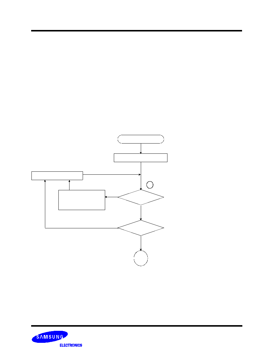
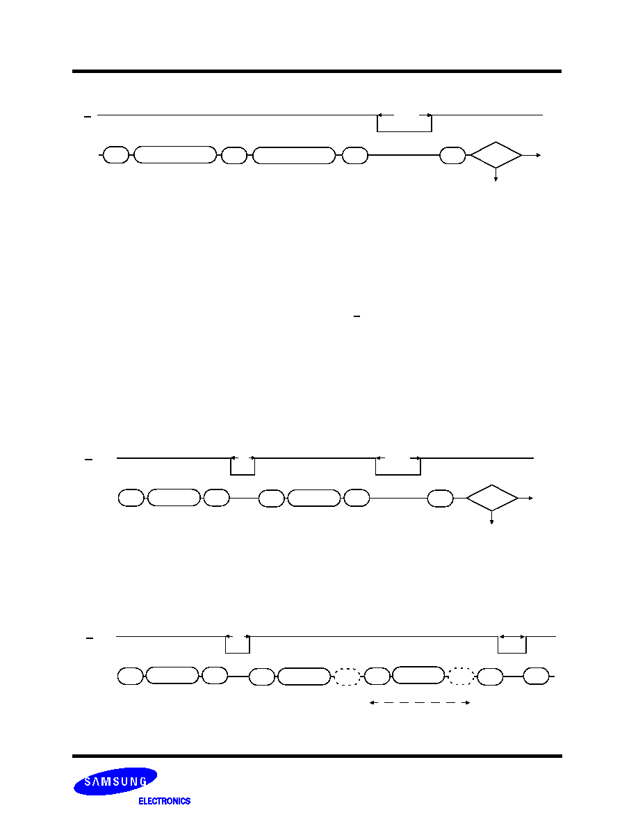
Identifying Initial Invalid Block(s)
Initial Invalid Block(s)
Initial invalid blocks are defined as blocks that contain one or more initial invalid bits whose reliability is not guaranteed by Samsung.
The information regarding the initial invalid block(s) is called the initial invalid block information. Devices with initial invalid block(s)
have the same quality level as devices with all valid blocks and have the same AC and DC characteristics. An initial invalid block(s)
does not affect the performance of valid block(s) because it is isolated from the bit line and the common source line by a select tran-
sistor. The system design must be able to mask out the initial invalid block(s) via address mapping. The 1st block, which is placed on
00h block address, is guaranteed to be a valid block, does not require Error Correction up to 1K program/erase cycles.
All device locations are erased(FFh) except locations where the initial invalid block(s) information is written prior to shipping. The ini-
tial invalid block(s) status is defined by the 1st byte in the spare area. Samsung makes sure that either the 1st or 2nd page of every
initial invalid block has non-FFh data at the column address of 2048. Since the initial invalid block information is also erasable in
most cases, it is impossible to recover the information once it has been erased. Therefore, the system must be able to recognize the
initial invalid block(s) based on the original initial invalid block information and create the initial invalid block table via the following
suggested flow chart(Figure 3). Any intentional erasure of the original initial invalid block information is prohibited.
*
Check "FFh" at the column address 2048
Figure 3. Flow chart to create initial invalid block table
Start
Set Block Address = 0
Check "FFh"
Increment Block Address
Last Block ?
End
No
Yes
Yes
Create (or update)
No
Initial
of the 1st and 2nd page in the block
Invalid Block(s) Table
FLASH MEMORY
14
Advance
K9F4G08U0M
K9K8G08U1M
NAND Flash Technical Notes
(Continued)
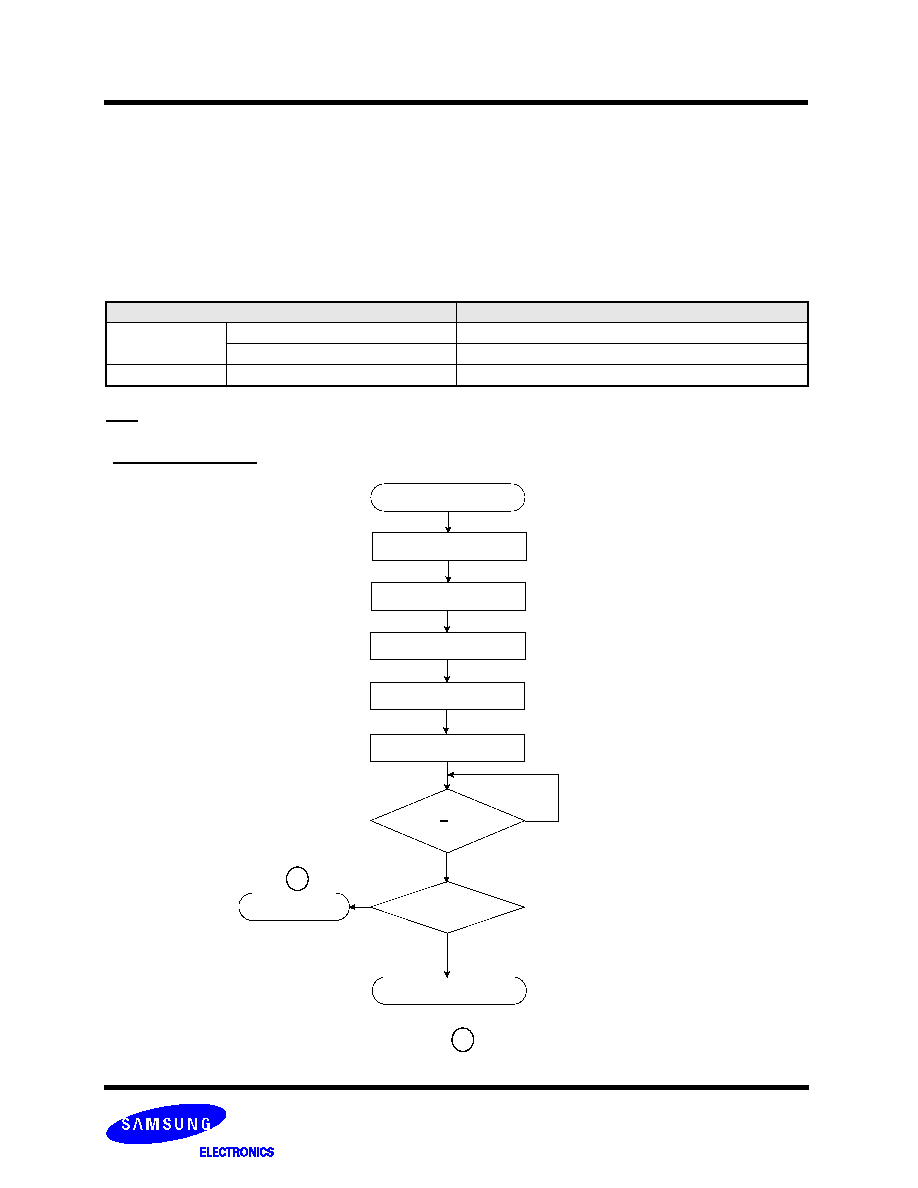
Program Flow Chart
Start
I/O 6 = 1 ?
I/O 0 = 0 ?
No
*
Write 80h
Write Address
Write Data
Write 10h
Read Status Register
Program Completed
or R/B = 1 ?
Program Error
Yes
No
Yes
: If program operation results in an error, map out
the block including the page in error and copy the
target data to another block.
*
Error in write or read operation
Within its life time, additional invalid blocks may develop with NAND Flash memory. Refer to the qualification report for the actual
data.The following possible failure modes should be considered to implement a highly reliable system. In the case of status read fail-
ure after erase or program, block replacement should be done. Because program status fail during a page program does not affect
the data of the other pages in the same block, block replacement can be executed with a page-sized buffer by finding an erased
empty block and reprogramming the current target data and copying the rest of the replaced block. In case of Read, ECC must be
employed. To improve the efficiency of memory space, it is recommended that the read or verification failure due to single bit error be
reclaimed by ECC without any block replacement. The said additional block failure rate does not include those reclaimed blocks.
Failure Mode
Detection and Countermeasure sequence
Write
Erase Failure
Status Read after Erase --> Block Replacement
Program Failure
Status Read after Program --> Block Replacement
Read
Single Bit Failure
Verify ECC -> ECC Correction
ECC
: Error Correcting Code --> Hamming Code etc.
Example) 1bit correction & 2bit detection
FLASH MEMORY
15
Advance
K9F4G08U0M
K9K8G08U1M
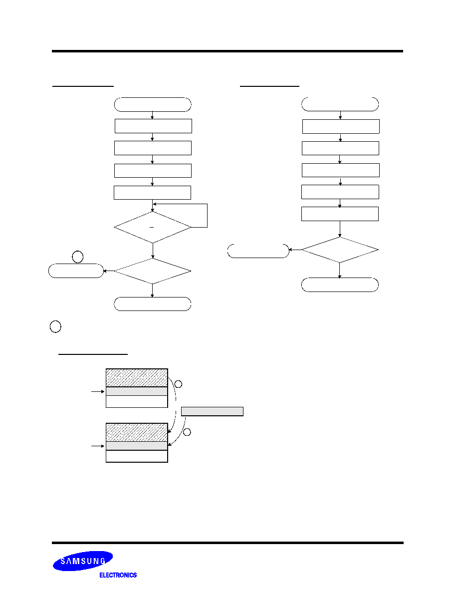
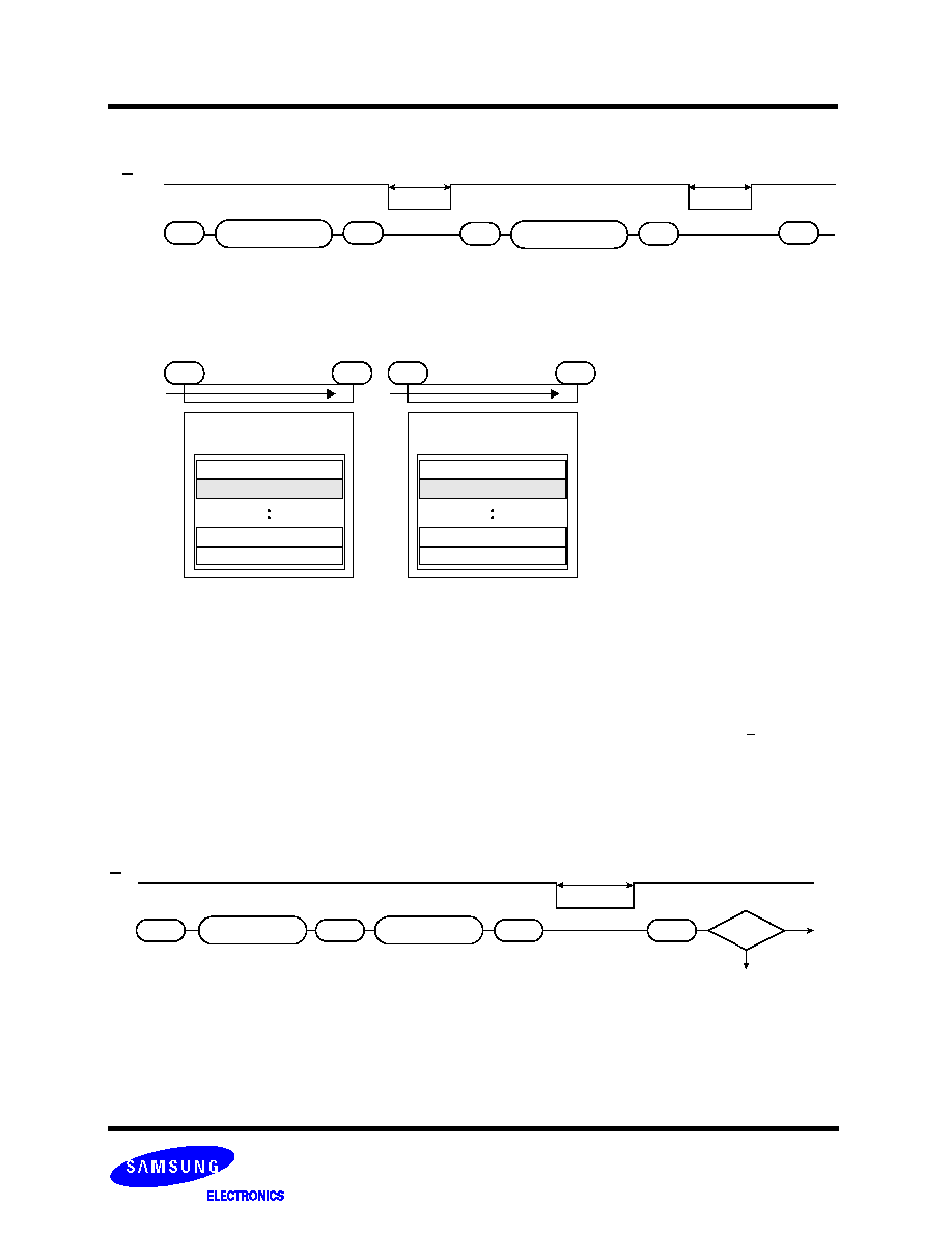
Erase Flow Chart
Start
I/O 6 = 1 ?
I/O 0 = 0 ?
No
*
Write 60h
Write Block Address
Write D0h
Read Status Register
or R/B = 1 ?
Erase Error
Yes
No
: If erase operation results in an error, map out
the failing block and replace it with another block.
*
Erase Completed
Yes
Read Flow Chart
Start
Verify ECC
No
Write 00h
Write Address
Read Data
ECC Generation
Reclaim the Error
Page Read Completed
Yes
NAND Flash Technical Notes
(Continued)
Write 30h
Block Replacement
* Step1
When an error happens in the nth page of the Block 'A' during erase or program operation.
* Step2
Copy the data in the 1st ~ (n-1)th page to the same location of another free block. (Block 'B')
* Step3
Then, copy the nth page data of the Block 'A' in the buffer memory to the nth page of the Block 'B'.
* Step4
Do not erase or program to Block 'A' by creating an 'invalid block' table or other appropriate scheme.
Buffer memory of the controller.
1st
Block A
Block B
(n-1)th
nth
(page)
{
1st
(n-1)th
nth
(page)
{
an error occurs.
1
2
FLASH MEMORY
16
Advance
K9F4G08U0M
K9K8G08U1M
NAND Flash Technical Notes
(Continued)
Copy-Back Operation with EDC & Plane Definition for EDC
Generally, copy-back program is very powerful to move data stored in a page without utilizing any external memory. But, if the source
page has a bit error for charge loss or charge gain, accumulated copy-back operations could also accumulate bit errors. For this rea-
son, two-bit ECC is recommanded for copy-back operation.
Because K9F4G08U0M supports Copy Back with EDC operation, only 1-bit ECC is sufficient for copy-back operation. During Copy-
Back operation, the system controller can detect a bit error for each 528-byte plane by monitoring the Status bits (I/O1 & I/O 2) of the
Status Register.
There are some restrictions against programming unit in copy-back operation with EDC. For enabling EDC operation, the page pro-
gram should be performed with the whole page unit (2,112-byte) or the each 528-byte plane unit. A page of 2,112-byte is composed
of 4 planes of 528-byte and each 528-byte plane is made up of 512-byte in the main area and 16-byte in the spare area.
"A" area
512 Byte
(1'st plane)
"H" area
(4'th plane)
Main Area (2,048 Byte)
16 Byte
"G" area
(3'rd plane)
16 Byte
"F" area
(2'nd plane)
16 Byte
"E" area
(1'st plane)
16 Byte
"B" area
512 Byte
(2'nd plane)
"C" area
512 Byte
(3'rd plane)
"D" area
512 Byte
(4'th plane)
Spare Area (64 Byte)
Table 2. Definition of the 528-Byte Plane
Plane
Main Area (Column 0~2,047)
Spare Area (Column 2,048~2,111)
Area Name
Column Address
Area Name
Column Address
1'st 528-Byte Plane
"A"
0 ~ 511
"E"
2,048 ~ 2,063
2'nd 528-Byte Plane
"B"
512 ~ 1,023
"F"
2,064 ~ 2,079
3'rd 528-Byte Plane
"C"
1,024 ~ 1,535
"G"
2,080 ~ 2,095
4'th 528-Byte Plane
"D"
1,536 ~ 2,047
"H"
2,096 ~ 2,111
Within a block, the pages must be programmed consecutively from the LSB (least significant bit) page of the block to MSB (most sig-
nificant bit) pages of the block. Random page address programming is prohibited.
From the LSB page to MSB page
DATA IN: Data (1)
Data (64)
(1)
(2)
(3)
(32)
(64)
Data register
Page 0
Page 1
Page 2
Page 31
Page 63
Ex.) Random page program (Prohibition)
DATA IN: Data (1)
Data (64)
(2)
(32)
(3)
(1)
(64)
Data register
Page 0
Page 1
Page 2
Page 31
Page 63
Addressing for program operation
:
:
:
:

FLASH MEMORY
17
Advance
K9F4G08U0M
K9K8G08U1M
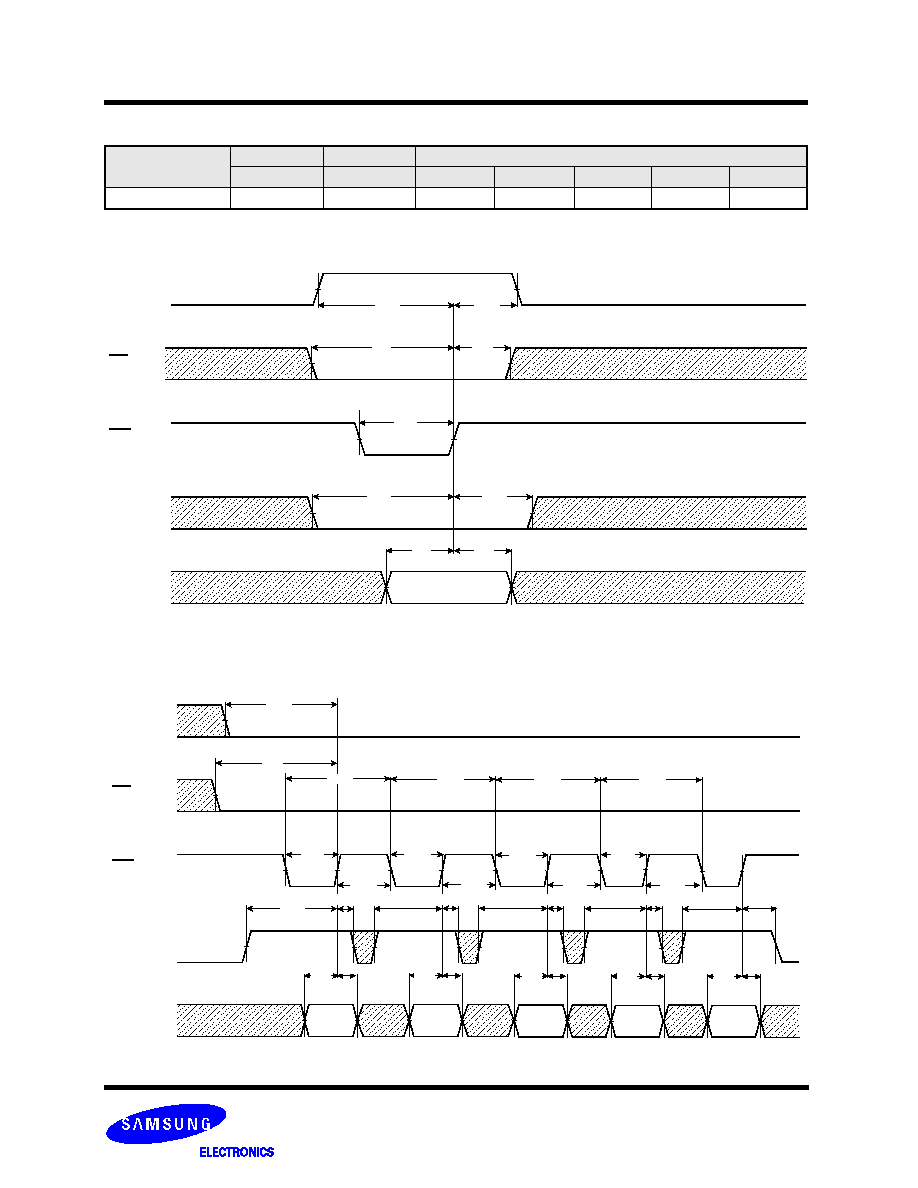
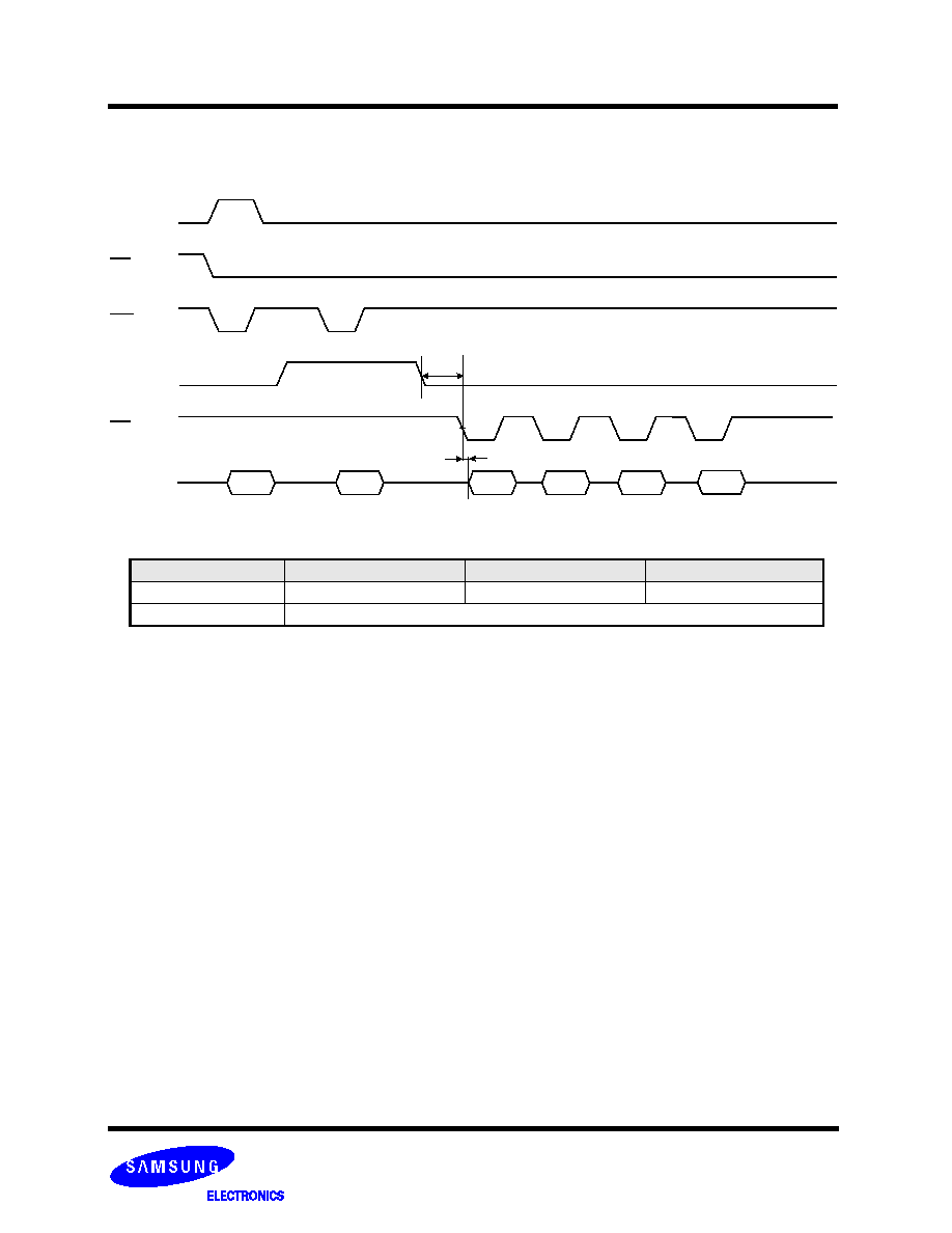
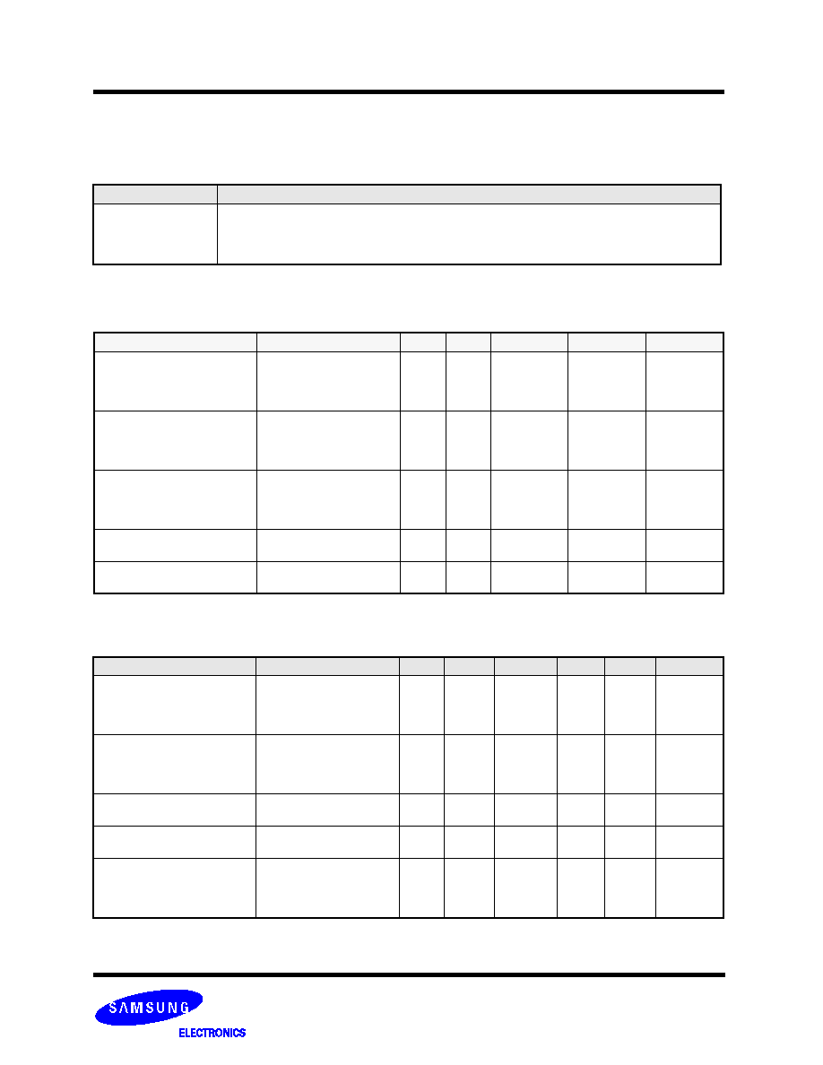
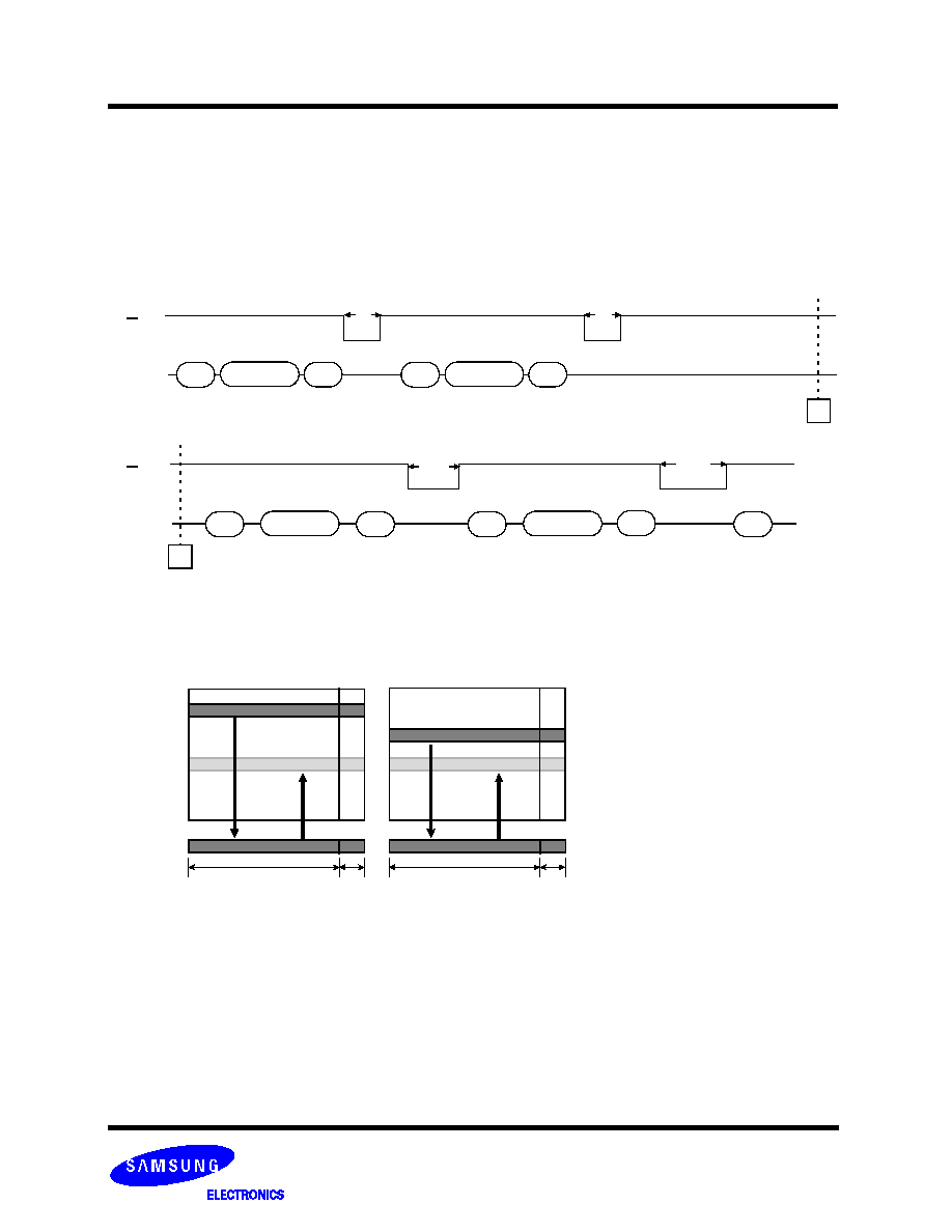
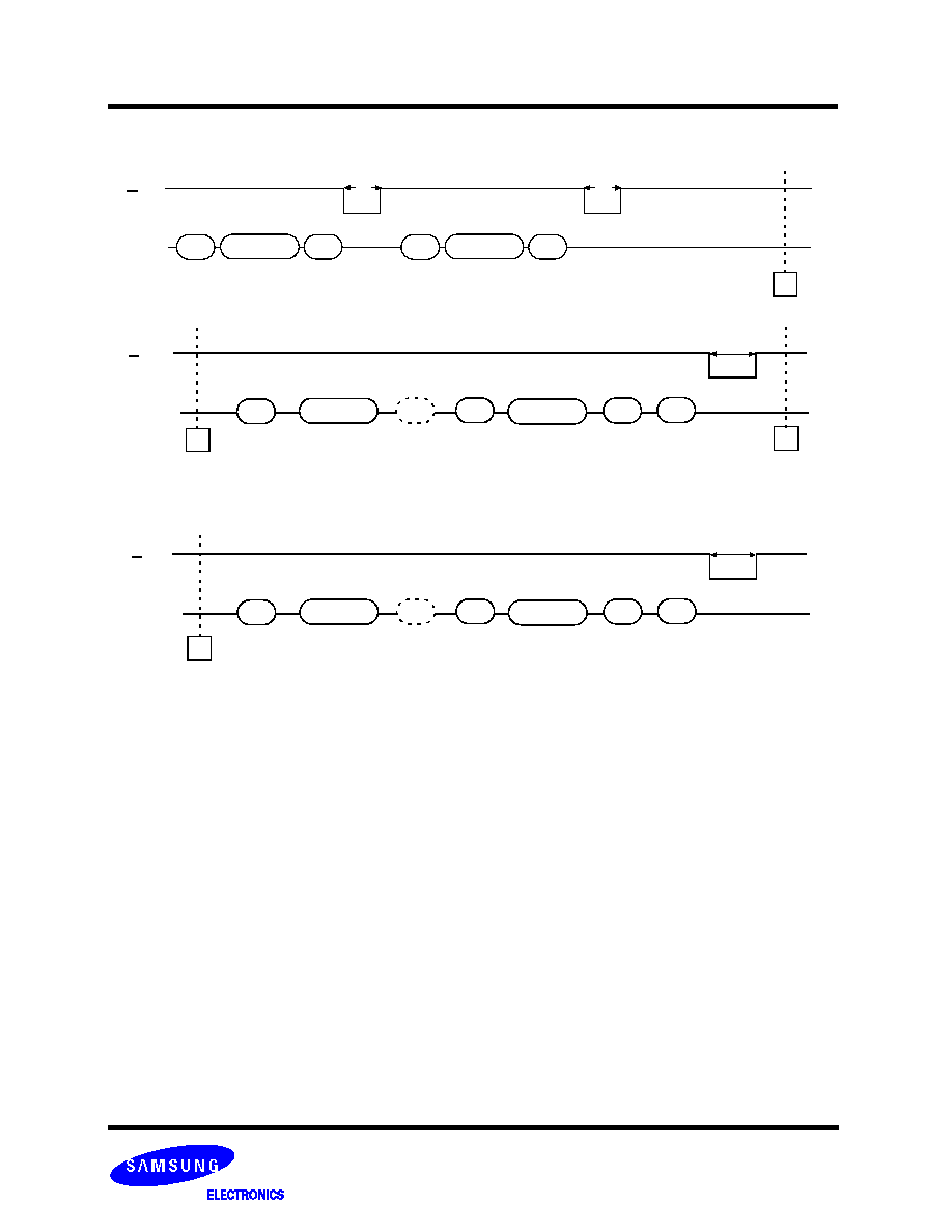
System Interface Using CE don't-care.
For an easier system interface, CE may be inactive during the data-loading or serial access as shown below. The internal 2,112byte
data registers are utilized as separate buffers for this operation and the system design gets more flexible. In addition, for voice or
audio applications which use slow cycle time on the order of u-seconds, de-activating CE during the data-loading and serial access
would provide significant savings in power consumption.
Figure 4. Program Operation with CE don't-care.
CE
WE
t
WP
t
CH
t
CS
Address(5Cycles)
80h
Data Input
CE
CLE
ALE
WE
Data Input
CE don't-care
10h
Address(5Cycle)
00h
CE
CLE
ALE
WE
Data Output(serial access)
CE don't-care
R/B
t
R
RE
t
CEA
out
t
REA
CE
RE
I/O
0
~
7
Figure 5. Read Operation with CE don't-care.
30h
I/Ox
I/Ox
FLASH MEMORY
18
Advance
K9F4G08U0M
K9K8G08U1M
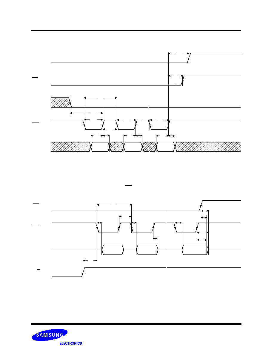
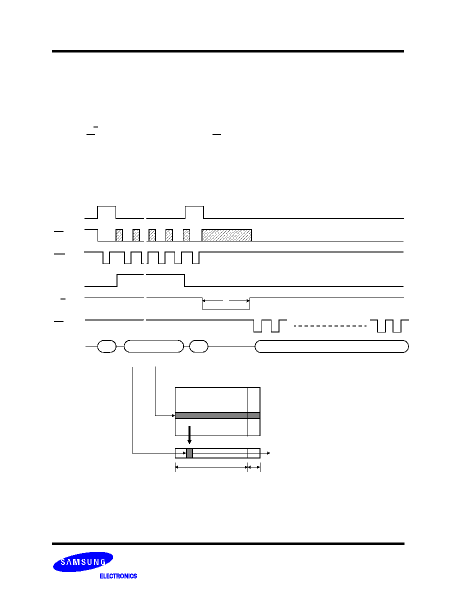
Command Latch Cycle
CE
WE
CLE
ALE
Command
Address Latch Cycle
t
CLS
t
CS
t
CLH
t
CH
t
WP
t
ALS
t
ALH
t
DS
t
DH
NOTE
Device
I/O
DATA
ADDRESS
I/Ox
Data In/Out
Col. Add1
Col. Add2
Row Add1
Row Add2
Row Add3
K9F4G08U0M
I/O 0 ~ I/O 7
2,112byte
A0~A7
A8~A11
A12~A19
A20~A27
A28~A29
I/Ox
CE
WE
CLE
ALE
Col. Add1
t
CS
t
WC
t
WP
t
ALS
t
DS
t
DH
t
ALH
t
ALS
t
WH
t
WC
t
WP
t
DS
t
DH
t
ALH
t
ALS
t
WH
t
WC
t
WP
t
DS
t
DH
t
ALH
t
ALS
t
WH
t
DS
t
DH
t
WP
I/Ox
Col. Add2
Row Add1
Row Add2
t
WC
t
WH
t
ALH
t
ALS
t
DS
t
DH
Row Add3
t
ALH
t
CLS
FLASH MEMORY
19
Advance
K9F4G08U0M
K9K8G08U1M
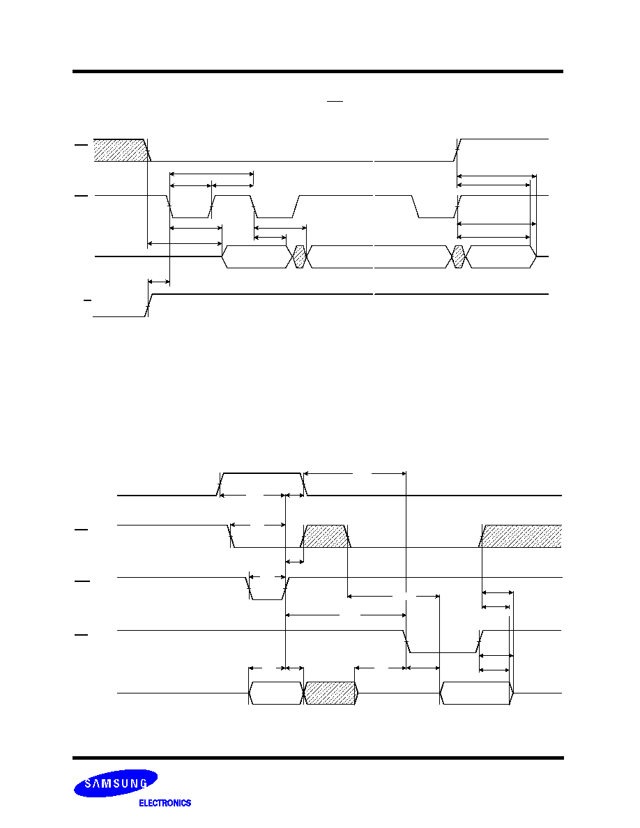
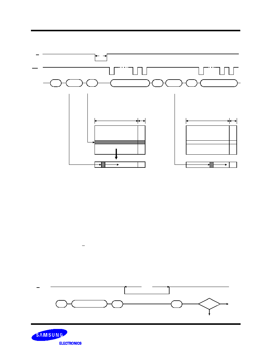
Input Data Latch Cycle
CE
CLE
WE
DIN 0
DIN 1
DIN final*
ALE
t
ALS
t
CLH
t
WC
t
CH
t
DS
t
DH
t
DS
t
DH
t
DS
t
DH
t
WP
t
WH
t
WP
t
WP
I/Ox
NOTES : DIN final means 2,112
* Serial Access Cycle after Read
(CLE=L, WE=H, ALE=L)
RE
CE
R/B
Dout
Dout
Dout
t
RC
t
REA
t
RR
t
RHOH
t
REA
t
REH
t
REA
t
COH
t
RHZ
I/Ox
t
CHZ
t
RHZ
NOTES : Transition is measured
±200mV from steady state voltage with load.
This parameter is sampled and not 100% tested.
tRLOH is valid when frequency is higher than 33MHz.
tRHOH starts to be valid when frequency is lower than 33MHz.
FLASH MEMORY
20
Advance
K9F4G08U0M
K9K8G08U1M
Status Read Cycle & EDC Status Read Cycle
CE
WE
CLE
RE
70h or 7Bh
Status Output
t
CLR
t
CLH
t
WP
t
CH
t
DS
t
DH
t
REA
t
IR
t
RHOH
t
COH
t
WHR
t
CEA
t
CLS
I/Ox
t
CHZ
t
RHZ
t
CS
RE
CE
R/B
I/Ox
t
RR
t
CEA
t
REA
t
RP
t
REH
t
RC
t
RHZ
t
CHZ
Serial Access Cycle after Read
(EDO Type, CLE=L, WE=H, ALE=L)
t
RHOH
t
COH
t
RLOH
Dout
Dout
t
REA
NOTES : Transition is measured
±200mV from steady state voltage with load.
This parameter is sampled and not 100% tested.
tRLOH is valid when frequency is higher than 33MHz.
tRHOH starts to be valid when frequency is lower than 33MHz.
FLASH MEMORY
21
Advance
K9F4G08U0M
K9K8G08U1M
Read Operation
(Intercepted by CE)
CE
CLE
R/B
WE
ALE
RE
Busy
00h
Dout N
Dout N+1
Dout N+2
Row Address
Column Address
t
WB
t
AR
t
CHZ
t
R
t
RR
t
RC
30h
Read Operation
CE
CLE
R/B
WE
ALE
RE
Busy
00h
Col. Add1
Col. Add2
Row Add1
Dout N
Dout N+1
Column Address
Row Address
t
WB
t
AR
t
R
t
RC
t
RHZ
t
RR
Dout M
t
WC
Row Add2
30h
t
CLR
I/Ox
I/Ox
Col. Add1
Col. Add2 Row Add1
Row Add2
Row Add3
Row Add3
t
C
OH
FLASH MEMORY
22
Advance
K9F4G08U0M
K9K8G08U1M
Ra
ndom Dat
a
Outpu
t
In a Page
CE
CLE
R/B
WE
ALE
RE
Busy
00h
Dout
N
D
out
N
+
1
Ro
w Addr
ess
Co
lumn
Addr
ess
t
W
B
t
AR
t
R
t
RR
t
R
C
30h
05h
Column Add
r
ess
Do
u
t
M
Do
u
t
M+
1
I
/Ox
C
o
l
.
A
dd1
Co
l
.
A
d
d
2
Ro
w Ad
d
1
Ro
w Ad
d2
C
o
l A
dd1
Co
l Ad
d2
Row Add
3
t
CLR
E0
h
t
WHR
t
REA
t
RHW
FLASH MEMORY
23
Advance
K9F4G08U0M
K9K8G08U1M
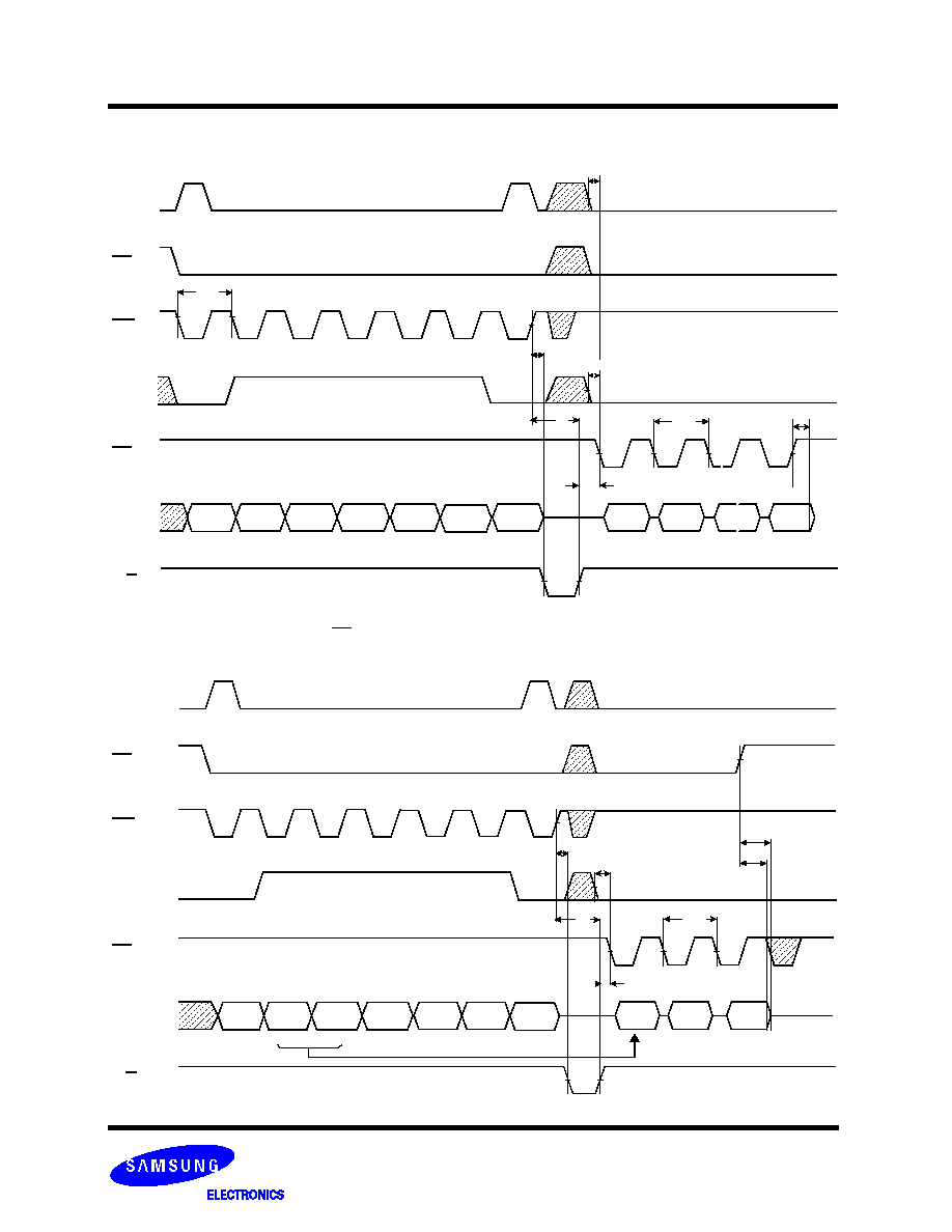
Page Program Operation
CE
CLE
R/B
WE
ALE
RE
80h
70h
I/O
0
Din
N
Din
10h
M
SerialData
Input Command Column Address
Row Address
1 up to m Byte
Serial Input
Program
Command
Read Status
Command
I/O
0
=0 Successful Program
I/O
0
=1 Error in Program
t
PROG
t
WB
t
WC
t
WC
t
WC
I/Ox
Co.l Add1 Col. Add2
Row Add1 Row Add2 Row Add3
NOTES : tADL is the time from the WE rising edge of final address cycle to the WE rising edge of first data cycle.
t
ADL
FLASH MEMORY
24
Advance
K9F4G08U0M
K9K8G08U1M
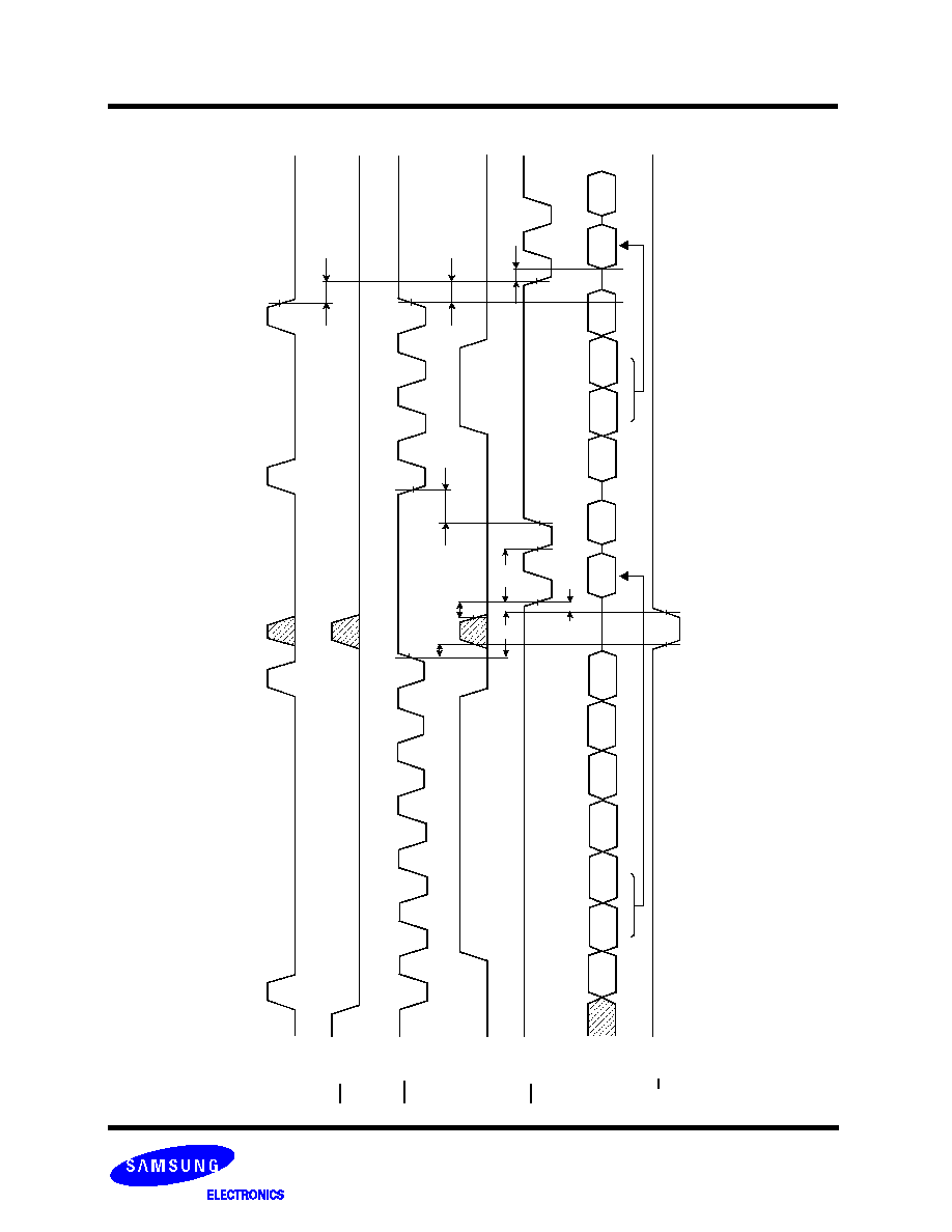
Pa
ge Program Operation with Rand
om Dat
a
In
put
CE
CLE
R/B
WE
ALE
RE
80
h
70
h
I/O
0
Di
n
N
Di
n
10h
M
Se
ri
al
D
a
ta
I
npu
t Command
Col
u
mn A
ddr
ess
R
ow
Addr
ess
Ser
i
al
I
nput
Pr
ogr
am
Co
mm
a
n
d
Re
ad Stat
us
Co
m
m
a
n
d
t
PR
O
G
t
WB
t
WC
t
WC
85
h
Rand
om Da
ta
I
nput
Co
mm
a
n
d
Col
u
mn Ad
dre
s
s
t
WC
Di
n
J
Din
K
Ser
i
al
In
put
I
/Ox
Col
.
A
dd1
Col
.
A
dd2
Row Add1
Row Add2
Col
.
A
dd1
Col
.
A
dd2
Row A
d
d
3
NOTES
:
1
.
tA
DL
is t
h
e
tim
e
fr
o
m
t
h
e
W
E
r
i
si
ng edge
of
fin
a
l addr
ess cycle
t
o
th
e
WE
r
i
sing edge
o
f
fi
rst dat
a cycle.
t
ADL
2.
For EDC
o
perat
ion
,
onl
y one
t
i
me ran
dom dat
a input
is
po
ssib
le at t
he sa
me addre
s
s.
t
ADL
FLASH MEMORY
25
Advance
K9F4G08U0M
K9K8G08U1M
Copy
-Ba
ck Program Operation
W
i
th
Ra
ndom Dat
a
Input
CE
CLE
R/B
WE
ALE
RE
00
h
I/O
x
85
h
Colu
mn
A
d
dr
ess
R
o
w A
d
dr
es
s
Re
ad
E
DC
S
t
at
us
or
Re
ad
S
t
at
us
Com
m
a
n
d
I/O
0
=
0
Succe
ssf
ul
Pr
og
ra
m
I/O
0
=1
Er
ro
r i
n
Pro
g
r
a
m
t
PROG
t
WB
t
WC
Busy
t
WB
t
R
Busy
10
h
Cop
y
-Back
Dat
a
I
n
pu
t C
o
mma
nd
35
h
Colu
m
n
A
d
dr
ess
Ro
w Ad
dress
D
a
ta
1
Dat
a
N
I
/Ox
Co
l
A
d
d
1
Co
l A
d
d
2
Ro
w A
d
d
1
Ro
w A
d
d
2
Co
l
A
d
d
1
Co
l A
d
d
2
Ro
w A
d
d
1
Ro
w A
d
d
2
Ro
w A
d
d
3
Ro
w A
d
d
3
7B
h
/
70
h
I/O
1 ~
I/
O
2
:
ED
C St
at
u
s
(
7
Bh
on
ly
)
N
O
TES :
1.
tA
DL is t
he ti
me
f
r
om t
he WE
rising edge of
final address
cycle t
o
the WE
rising
ed
ge
of
f
i
rst
da
ta
cycl
e
.
t
ADL
2.
F
o
r
E
DC
op
erat
ion
,
only one
t
i
me rand
om dat
a
i
nput
is po
ssibl
e
a
t
ht
e
same ad
dress.
FLASH MEMORY
26
Advance
K9F4G08U0M
K9K8G08U1M
BLOCK ERASE OPERATION
CE
CLE
R/B
WE
ALE
RE
60h
Erase Command
Read Status
Command
I/O
0
=1 Error in Erase
D0h
70h
I/O 0
Busy
t
WB
t
BERS
I/O
0
=0 Successful Erase
Row Address
t
WC
Auto Block Erase
Setup Command
I/Ox
Row Add1 Row Add2 Row Add3
FLASH MEMORY
27
Advance
K9F4G08U0M
K9K8G08U1M
T
w
o
-
Pl
ane Page
Program
Ope
r
a
t
ion
80h
I/
O
0
~
7
R/B
11h
Ex
.)
Tw
o-P
l
a
n
e
Pa
ge
P
r
o
g
ra
m
t
DBS
Y
Addr
ess & Dat
a
Inp
u
t
81
h
10
h
Ad
dress &
Dat
a
I
nput
70
h
t
PRO
G
Col Add1
,2 & Row Add 1,
2,
3
2
112 Byt
e
Da
ta
CE
CLE
R/B
WE
ALE
RE
80h
Di
n N
Di
n
11h
M
S
e
r
i
al Data
Input Com
m
and
C
o
l
u
mn A
d
dr
es
s
P
r
ogr
am
tD
BS
Y
tW
B
tW
C
Comm
and
(Dum
m
y
)
Di
n
N
10h
tPROG
tW
B
I/
O
Pro
g
ra
m Co
n
f
ir
m
C
o
mma
nd
(Tr
ue)
81
h
70h
Page Row Add
r
es
s
I
/Ox
1 u
p
t
o
2
1
12
Byt
e
Da
ta
Ser
i
al
I
n
pu
t
Di
n
M
Read Statu
s
Command
t
DBSY
:
ty
p. 500ns
m
a
x. 1
µ
s
Co
l
A
d
d1
Col
Add2
R
o
w A
d
d1
Row A
dd2
Ro
w
A
d
d
3
C
o
l
Add1
Col
A
dd2
Row A
d
d1
Row
A
d
d2
Ro
w A
d
d3
Co
l
A
dd1,
2 & Row
A
dd 1,
2,3
21
12 Byte
Dat
a
A
0
~
A
11 :
V
a
lid
A
12
~
A
1
7
:
Fixe
d 'Low'
A
1
8
:
Fixed 'Lo
w
'
A
19
~
A
29
:
Fixed 'Low'
A
0
~
A
11
:
Valid
A
12
~
A
17
:
V
a
lid
A
1
8
:
Fixed 'High
'
A
19
~
A
29
:
V
a
lid
FLASH MEMORY
28
Advance
K9F4G08U0M
K9K8G08U1M
Two-Plane Block Erase Operation
Block Erase Setup Command
Erase Confirm Command
Read Status Command
2 times repeat
60h
Row Add1,2,3
I/O
0
~
7
R/B
60h
A
9
~ A
25
D0h
t
BERS
* For Two-Plane Erase operation, Block address to be erased should be repeated before "D0H" command.
Ex.) Two-Plane Block Erase Operation
CE
CLE
R/B
I/O
X
WE
ALE
RE
60h
Row Add1
D0h
70h
I/O 0
Busy
t
WB
t
BERS
Row Address
t
WC
D0h
70h
Address
Address
Row Add1,2,3
I/O 0 = 0 Successful Erase
I/O 1 =1 Error in Erase
Row Add2 Row Add3
A
12
~ A
17 :
Fixed 'Low'
A
18 :
Fixed 'Low'
A
19
~ A
29 :
Fixed 'Low'
A
12
~ A
17 :
Fixed 'Low'
A
18 :
Fixed 'High'
A
19
~ A
29 :
valid
FLASH MEMORY
29
Advance
K9F4G08U0M
K9K8G08U1M
Read ID Operation
CE
CLE
WE
ALE
RE
90h
Read ID Command
Maker Code Device Code
00h
ECh
Device
t
REA
Address 1cycle
4th cyc.*
I/Ox
t
AR
Device
Device Code*(2nd Cycle)
3rd Cycle*
4th Cycle*
K9F4G08U0M
DCh
10h
95h
K9K8G08U1M
Same as each K9F4G08U0M in it
Code*
3rd cyc.*
FLASH MEMORY
30
Advance
K9F4G08U0M
K9K8G08U1M
4th ID Data
Description
I/O7
I/O6
I/O5 I/O4
I/O3
I/O2
I/O1 I/O0
Page Size
(w/o redundant area )
1KB
2KB
Reserved
Reserved
0 0
0 1
1 0
1 1
Block Size
(w/o redundant area )
64KB
128KB
256KB
Reserved
0 0
0 1
1 0
1 1
Redundant Area Size
( byte/512byte)
8
16
0
1
Organization
x8
x16
0
1
Serial AccessMinimum
50ns
25ns
Reserved
Reserved
0
1
0
1
0
0
1
1
ID Definition Table
90 ID : Access command = 90H
Description
1
st
Byte
2
nd
Byte
3
rd
Byte
4
th
Byte
Maker Code
Device Code
Internal Chip Number, Cell Type, Number of Simultaneously Programed Pages, Etc
Page Size, Block Size,Redundant Area Size, Organization, Serial Access Minimum
3rd ID Data
Description
I/O7
I/O6
I/O5 I/O4
I/O3 I/O2
I/O1 I/O0
Internal Chip Number
1
2
4
8
0 0
0 1
1 0
1 1
Cell Type
2 Level Cell
4 Level Cell
8 Level Cell
16 Level Cell
0 0
0 1
1 0
1 1
Number of
Simultaneously
Programmed Pages
1
2
4
8
0 0
0 1
1 0
1 1
Interleave Program
Between multiple chips
Not Support
Support
0
1
Cache Program
Not Support
Support
0
1
FLASH MEMORY
31
Advance
K9F4G08U0M
K9K8G08U1M
Device Operation
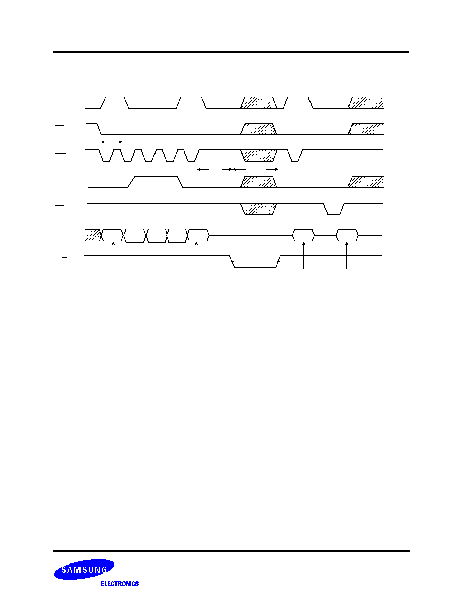
PAGE READ
Read mode is initiated by writing 00h-30h to the command register along with five address cycles. In two consecutive read opera-
tions, the second one doesn't need 00h command, which five address cycles and 30h command initiates that operation. Once the
command is latched, it does not need to be written for the following page read operation. Two types of operations are available : ran-
dom read out, serial page read out.
The random read mode is enabled when the page address is changed. The 2,112 bytes of data within the selected page are trans-
ferred to the data registers in less than 20
µs(t
R
). The system controller can detect the completion of this data transfer(tR) by analyzing
the output of R/B pin. Once the data in a page is loaded into the data registers, they may be read out in 25ns cycle time by sequen-
tially pulsing RE. The repetitive high to low transitions of the RE clock make the device output the data starting from the selected col-
umn address up to the last column address.
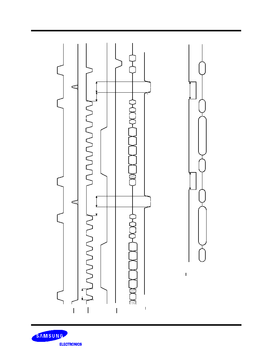
The device may output random data in a page instead of the consecutive sequential data by writing random data output command.
The column address of next data, which is going to be out, may be changed to the address which follows random data output com-
mand. Random data output can be operated multiple times regardless of how many times it is done in a page.
Figure 6. Read Operation
Address(5Cycle)
00h
Col. Add.1,2 & Row Add.1,2,3
Data Output(Serial Access)
Data Field
Spare Field
CE
CLE
ALE
R/B
WE
RE
t
R
30h
I/Ox
FLASH MEMORY
32
Advance
K9F4G08U0M
K9K8G08U1M
Figure 7. Random Data Output In a Page
Address
00h
Data Output
R/B
RE
t
R
30h
Address
05h
E0h
5Cycles
2Cycles
Data Output
Data Field
Spare Field
Data Field
Spare Field
I/Ox
Col. Add.1,2 & Row Add.1,2,3
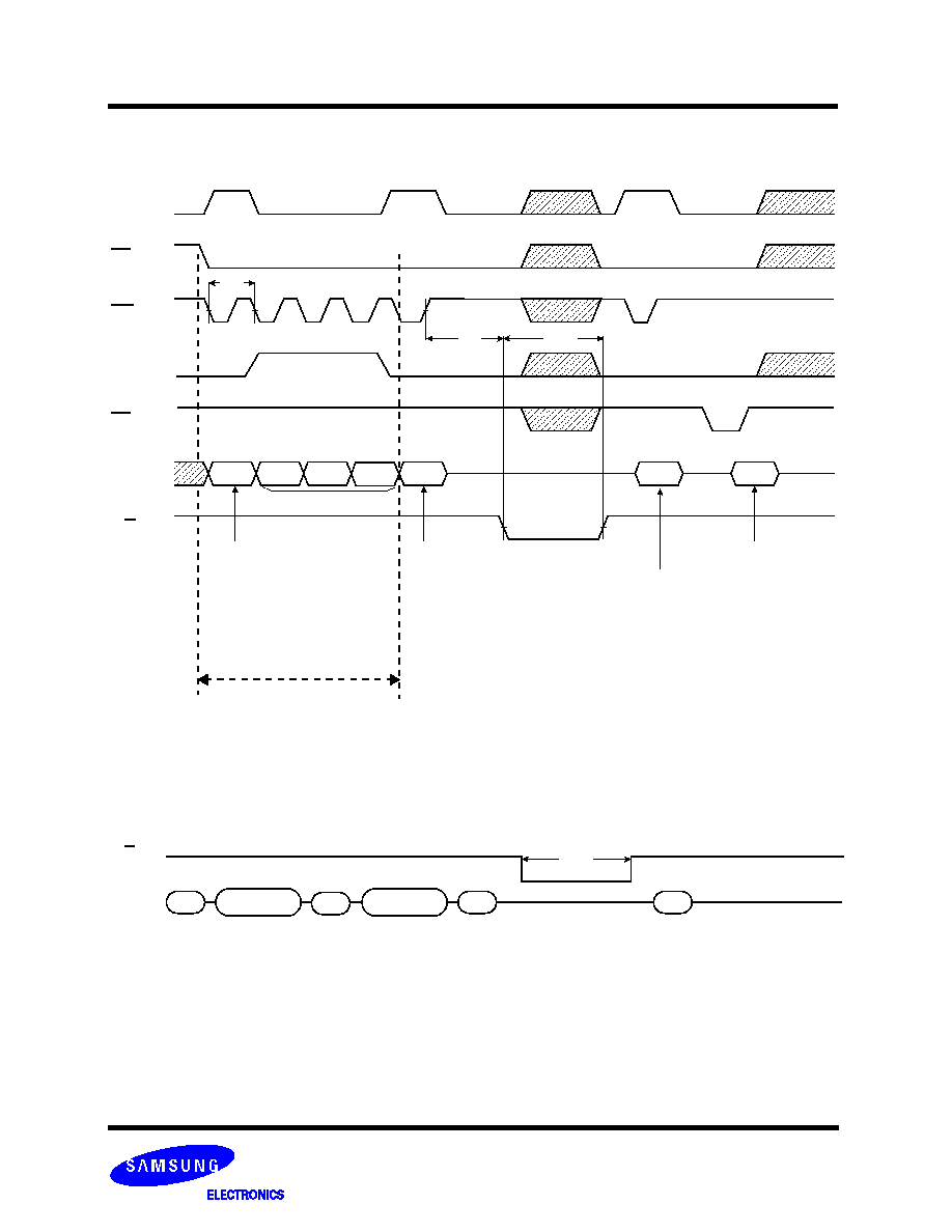
PAGE PROGRAM
The device is programmed basically on a page basis, but it does allow multiple partial page programing of a word or consecutive
bytes up to 2,112, in a single page program cycle. The number of consecutive partial page programming operation within the same
page without an intervening erase operation must not exceed 4 times for main array(1time/512byte) and 4 times for spare
array(1time/16byte). The addressing should be done in sequential order in a block. A page program cycle consists of a serial data
loading period in which up to 2,112bytes of data may be loaded into the data register, followed by a non-volatile programming period
where the loaded data is programmed into the appropriate cell.
The serial data loading period begins by inputting the Serial Data Input command(80h), followed by the five cycle address inputs and
then serial data loading. The words other than those to be programmed do not need to be loaded. The device supports random data
input in a page. The column address for the next data, which will be entered, may be changed to the address which follows random
data input command(85h). Random data input may be operated multiple times regardless of how many times it is done in a page.
The Page Program confirm command(10h) initiates the programming process. Writing 10h alone without previously entering the
serial data will not initiate the programming process. The internal write state controller automatically executes the algorithms and tim-
ings necessary for program and verify, thereby freeing the system controller for other tasks. Once the program process starts, the
Read Status Register command may be entered to read the status register. The system controller can detect the completion of a pro-
gram cycle by monitoring the R/B output, or the Status bit(I/O 6) of the Status Register. Only the Read Status command and Reset
command are valid while programming is in progress. When the Page Program is complete, the Write Status Bit(I/O 0) may be
checked(Figure 8). The internal write verify detects only errors for "1"s that are not successfully programmed to "0"s. The command
register remains in Read Status command mode until another valid command is written to the command register.
Figure 8. Program & Read Status Operation
80h
R/B
Address & Data Input
I/O
0
Pass
Data
10h
70h
Fail
t
PROG
I/Ox
Col. Add.1,2 & Row Add.1,2,3
"0"
"1"
Col. Add.1,2
FLASH MEMORY
33
Advance
K9F4G08U0M
K9K8G08U1M
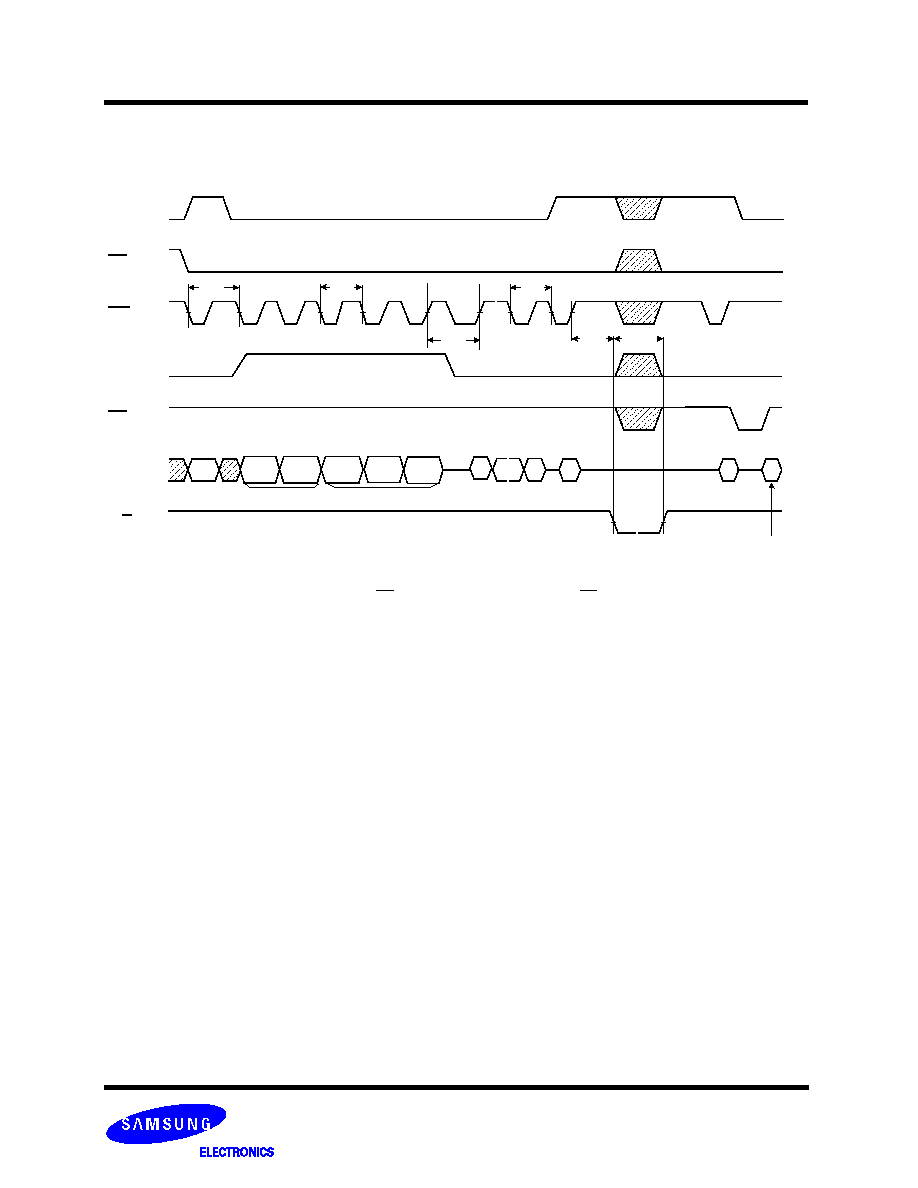
Figure 9. Random Data Input In a Page
80h
R/B
Address & Data Input
I/O
0
Pass
10h
70h
Fail
t
PROG
85h
Address & Data Input
I/Ox
Col. Add.1,2 & Row Add1,2,3
Col. Add.1,2
Data
Data
"0"
"1"
Copy-Back Program
The Copy-Back program is configured to quickly and efficiently rewrite data stored in one page without utilizing an external memory.
Since the time-consuming cycles of serial access and re-loading cycles are removed, the system performance is improved. The ben-
efit is especially obvious when a portion of a block is updated and the rest of the block also need to be copied to the newly assigned
free block. The operation for performing a copy-back program is a sequential execution of page-read without serial access and copy-
ing-program with the address of destination page. A read operation with "35h" command and the address of the source page moves
the whole 2,112-byte data into the internal data buffer. As soon as the device returns to Ready state, Page-Copy Data-input com-
mand (85h) with the address cycles of destination page followed may be written. The Program Confirm command (10h) is required to
actually begin the programming operation. During tPROG, the device executes EDC of itself. Once the program process starts, the
Read Status Register command (70h) or Read EDC Status command (7Bh) may be entered to read the status register. The system
controller can detect the completion of a program cycle by monitoring the R/B output, or the Status bit(I/O 6) of the Status Register.
When the Copy-Back Program is complete, the Write Status Bit(I/O 0) and EDC Status Bits (I/O 1 ~ I/O 4) may be checked(Figure 10
& Figure 11& Figure 12). The internal write verification detects only errors for "1"s that are not successfully programmed to "0"s and
the internal EDC checks whether there is only 1-bit error for each 528-byte plane of the source page. More than 2-bit error detection
is not available for each 528-byte plane. The command register remains in Read Status command mode or Read EDC Status com-
mand mode until another valid command is written to the command register.
During copy-back program, data modification is possible using random data input command (85h) as shown in Figure11. But EDC
status Bits are not available during copy back for some bits or bytes modified by Random Data Input operation.
However, in case of the 528 byte plane unit modification, EDC status bits are abailable.
Figure 10. Page Copy-Back program Operation
00h
R/B
Add.(5Cycles)
I/O
0
Pass
85h
70h
Fail
t
PROG
Add.(5Cycles)
t
R
Source Address
Destination Address
35h
10h
I/Ox
Col. Add.1,2 & Row Add.1,2,3
Col. Add.1,2 & Row Add.1,2,3
Figure 11. Page Copy-Back program Operation with Random Data Input
00h
R/B
Add.(5Cycles)
85h
70h
t
PROG
Add.(5Cycles)
t
R
Source Address
Destination Address
Data
35h
10h
85h
Data
Add.(2Cycles)
There is no limitation for the number of repetition.
I/Ox
Col. Add.1,2 & Row Add.1,2,3
Col. Add.1,2 & Row Add.1,2,3
Col. Add.1,2
Note: 1. For EDC operation, only one time random data input is possible at the same address.
Note
:
1. Copy-Back Program operation is allowed only within the same memory plane.
2. On the same plane, It's prohibited to operate copy-back program from an odd address page(source page) to an even
address page(target page) or from an even address page(source page) to an odd address page(target page).
Therefore, the copy-back program is permitted just between odd address pages or even address pages.
FLASH MEMORY
34
Advance
K9F4G08U0M
K9K8G08U1M
Figure 12. Page Copy-Back program Operation with EDC & Read EDC Status
00h
R/B
Add.(5Cycles)
85h
7Bh
t
PROG
Add.(5Cycles)
t
R
Source Address
Destination Address
35h
10h
I/Ox
Col. Add.1,2 & Row Add.1,2,3
Col. Add.1,2 & Row Add.1,2,3
EDC Status Output
Figure 13. Block Erase Operation
BLOCK ERASE
The Erase operation is done on a block basis. Block address loading is accomplished in three cycles initiated by an Erase Setup
command(60h). Only address A
18
to A
29
is valid while A
12
to A
17
is ignored. The Erase Confirm command(D0h) following the block
address loading initiates the internal erasing process. This two-step sequence of setup followed by execution command ensures that
memory contents are not accidentally erased due to external noise conditions.
At the rising edge of WE after the erase confirm command input, the internal write controller handles erase and erase-verify. When
the erase operation is completed, the Write Status Bit(I/O 0) may be checked. Figure 13 details the sequence.
60h
Row Add 1,2,3
R/B
Address Input(3Cycle)
I/O
0
Pass
D0h
70h
Fail
t
BERS
I/Ox
"0"
"1"
EDC OPERATION
Note that the user who use Copy-Back with EDC mode, only one time random data input is possible at the same address during
Copy-Back program or page program mode. For the user who use Copy-Back without EDC, there is no limitation for the random data
input at the same address.
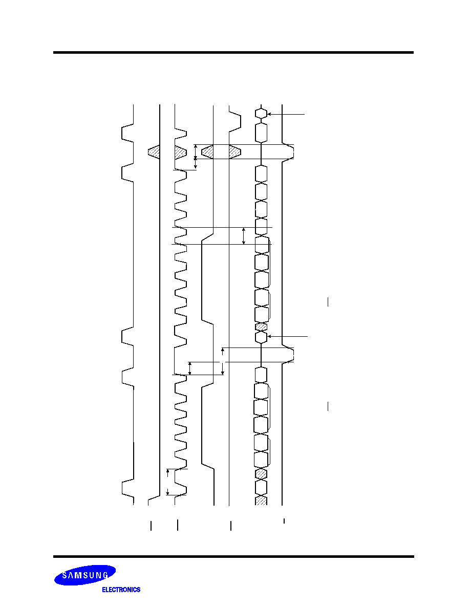
Two-Plane Page Program
Two-Plane Page Program is an extension of Page Program, for a single plane with 2112 byte page registers. Since the device is
equipped with two memory planes, activating the two sets of 2112 byte page registers enables a simultaneous programming of two
pages.
After writing the first set of data up to 2112 byte into the selected page register, Dummy Page Program command (11h) instead of
actual Page Program (10h) is inputted to finish data-loading of the first plane. Since no programming process is involved, R/B
remains in Busy state for a short period of time(tDBSY). Read Status command (70h) may be issued to find out when the device
returns to Ready state by polling the Ready/Busy status bit(I/O 6). Then the next set of data for the other plane is inputted after the
81h command and address sequences. After inputting data for the last plane, actual True Page Program(10h) instead of dummy
Page Program command (11h) must be followed to start the programming process. The operation of R/B and Read Status is the
same as that of Page Program. Althougth two planes are programmed simultaneously, pass/fail is not available for each page when
the program operation completes. Status bit of I/O 0 is set to "1" when any of the pages fails.
Restriction in addressing with Two-Plane Page Program is shown is Figure14.
FLASH MEMORY
35
Advance
K9F4G08U0M
K9K8G08U1M
Figure 14. Two-Plane Page Program
80h
11h
Data
Input
Plane 0
(2048 Block)
Block 0
Block 2
Block 4094
Block 4092
80h
I/O
0 ~ 7
R/B
Address & Data Input
11h
81h
10h
t
DBSY
t
PROG
70h
Address & Data Input
NOTE : It is noticeable that same row address except for A
18
is applied to the two blocks
81h
10h
Plane 1
(2048 Block)
Block 1
Block 3
Block 4095
Block 4093
Figure 15. Two-Plane Block Erase Operation
60h
I/O
X
R/B
60h
D0h
I/O
Pass
Fail
t
BERS
Address (3 Cycle)
Address (3 Cycle)
70h
"0"
"1"
A
12
~ A
17 :
Fixed 'Low'
A
18 :
Fixed 'Low'
A
19
~ A
29 :
Fixed 'Low'
A
12
~ A
17 :
Fixed 'Low'
A
18 :
Fixed 'High'
A
19
~ A
29 :
valid
Two-Plane Block Erase
Basic concept of Two-Plane Block Erase operation is identical to that of Two-Plane Page Program. Up to two blocks, one from each
plane can be simultaneously erased. Standard Block Erase command sequences (Block Erase Setup command(60h) followed by
three address cycles) may be repeated up to twice for erasing up to two blocks. Only one block should be selected from each plane.
The Erase Confirm command(D0h) initiates the actual erasing process. The completion is detected by monitoring R/B pin or Ready/
Busy status bit (I/O 6).
A
0
~ A
11 :
Valid
A
12
~ A
17 :
Fixed 'Low'
A
18 :
Fixed 'Low'
A
19
~ A
29 :
Fixed 'Low'
A
0
~ A
11 :
Valid
A
12
~ A
17 :
Valid
A
18 :
Fixed 'High'
A
19
~ A
29 :
Valid
FLASH MEMORY
36
Advance
K9F4G08U0M
K9K8G08U1M
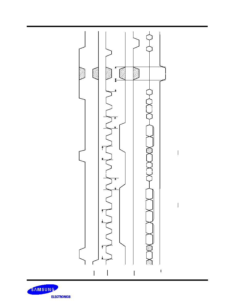
Figure 16. Two-Plane Copy-Back program Operation
R/B
85h
70h
t
PROG
Add.(5Cycles)
Destination Address
10h
I/Ox
Col. Add.1,2 & Row Add.1,2,3
81h
Add.(5Cycles)
Destination Address
Col. Add.1,2 & Row Add.1,2,3
00h
R/B
Add.(5Cycles)
t
R
Source Address On Plane0
35h
I/Ox
Col. Add.1,2 & Row Add.1,2,3
00h
Add.(5Cycles)
Source Address On Plane1
35h
Col. Add.1,2 & Row Add.1,2,3
t
R
11h
t
DBSY
Two-Plane Copy-Back Page Program
Two-Plane Copy-Back Page Program is an extension of Copy-Back Program, for a single plane with 2112 byte page registers. Since
the device is equipped with two memory planes, activating the two sets of 2112 byte page registers enables a simultaneous pro-
gramming of two pages.
Data Field
Spare Field
Data Field
Spare Field
(1)
(2)
(3)
(3)
Plane0
Plane1
Source page
Target page
Source page
Target page
(1) : Read Copy Back On Plane0
(2) : Read Copy Back On Plane1
(3) : Two-Plane Copy-Back Page Program
A
0
~ A
11 :
Fixed 'Low'
A
12
~ A
17 :
Fixed 'Low'
A
18 :
Fixed 'Low'
A
19
~ A
29 :
Fixed 'Low'
A
0
~ A
11 :
Fixed 'Low'
A
12
~ A
17 :
Valid
A
18 :
Fixed 'High'
A
19
~ A
29 :
Valid
1
1
Note
:
1. Copy-Back Program operation is allowed only within the same memory plane.
2. On the same plane, It's prohibited to operate copy-back program from an odd address page(source page) to an even
address page(target page) or from an even address page(source page) to an odd address page(target page).
Therefore, the copy-back program is permitted just between odd address pages or even address pages.
FLASH MEMORY
37
Advance
K9F4G08U0M
K9K8G08U1M
R/B
85h
11h
t
DBSY
Add.(5Cycles)
Data
85h
Data
I/Ox
Col. Add.1,2 & Row Add.1,2,3
Col. Add.1,2
Add.(2Cycles)
00h
R/B
Add.(5Cycles)
t
R
Source Address On Plane0
35h
I/Ox
Col. Add.1,2 & Row Add.1,2,3
00h
Add.(5Cycles)
Source Address On Plane1
35h
Col. Add.1,2 & Row Add.1,2,3
t
R
1
R/B
85h
10h
t
PROG
Add.(5Cycles)
Data
85h
Data
I/Ox
Col. Add.1,2 & Row Add.1,2,3
Col. Add.1,2
Add.(2Cycles)
1
2
2
Destination Address
A
0
~ A
11 :
Valid
A
12
~ A
17 :
Fixed 'Low'
A
18 :
Fixed 'Low'
A
19
~ A
29 :
Fixed 'Low'
Destination Address
A
0
~ A
11 :
Valid
A
12
~ A
17 :
Valid
A
18 :
Fixed 'High'
A
19
~ A
29 :
Valid
Figure 17. Two-Plane Copy-Back program Operation with Random Data Input
Note
:
1. Copy-Back Program operation is allowed only within the same memory plane.
2. On the same plane, It's prohibited to operate copy-back program from an odd address page(source page) to an even
address page(target page) or from an even address page(source page) to an odd address page(target page).
Therefore, the copy-back program is permitted just between odd address pages or even address pages.
3. EDC status Bits are not available during copy back for some bits or bytes modified by Random Data Input operation.
in case of the 528 byte plane unit modification, EDC status bits are abailable
FLASH MEMORY
38
Advance
K9F4G08U0M
K9K8G08U1M
READ STATUS
The device contains a Status Register which may be read to find out whether program or erase operation is completed, and whether
the program or erase operation is completed successfully. After writing 70h command to the command register, a read cycle outputs
the content of the Status Register to the I/O pins on the falling edge of CE or RE, whichever occurs last. This two line control allows
the system to poll the progress of each device in multiple memory connections even when R/B pins are common-wired. RE or CE
does not need to be toggled for updated status. Refer to Table 3 for specific Status Register definitions. The command register
remains in Status Read mode until further commands are issued to it. Therefore, if the status register is read during a random read
cycle, the read command(00h) should be given before starting read cycles.
Table 3. Staus Register Definition for 70h Command
NOTE :
1. I/Os defined 'Not use' are recommended to be masked out when Read Status is being executed.
I/O
Page Program
Block Erase
Read
Definition
I/O 0
Pass/Fail
Pass/Fail
Not use
Pass : "0" Fail : "1"
I/O 1
Not use
Not use
Not use
Don't -cared
I/O 2
Not use
Not use
Not use
Don't -cared
I/O 3
Not Use
Not Use
Not Use
Don't -cared
I/O 4
Not Use
Not Use
Not Use
Don't -cared
I/O 5
Not Use
Not Use
Not Use
Don't -cared
I/O 6
Ready/Busy
Ready/Busy
Ready/Busy
Busy : "0" Ready : "1"
I/O 7
Write Protect
Write Protect
Write Protect
Protected : "0" Not Protected : "1"
READ EDC STATUS
Read EDC status operation is only available on 'Copy Back Program'. The device contains a EDC Status Register which may be
read to find out whether there is error during 'Read for Copy Back'. After writing 7Bh command to the command register, a read cycle
outputs the content of the EDC Status Register to the I/O pins on the falling edge of CE or RE, whichever occurs last. This two line
control allows the system to poll the progress of each device in multiple memory connections even when R/B pins are common-wired.
RE or CE does not need to be toggled for updated status. Refer to Table 4 for specific Status Register definitions. The command reg-
ister remains in EDC Status Read mode until further commands are issued to it.
Table 4. Status Register Definition for 7Bh Command
NOTE :
1. I/Os defined 'Not use' are recommended to be masked out when Read Status is being executed.
2. More than 2-bit error detection isn't available for each 528B plane.
That is to say, only 1-bit error detection is avaliable for each 528B plane.
I/O
Copy Back Program
Page Program Block Erase
Read
Definition
I/O 0
Pass/Fail of Copy Back Program
Pass/Fail
Pass/Fail
Not use
Pass : "0", Fail : "1"
I/O 1
EDC Status
Not use
Not use
Not use
No Error : "0", Error : "1"
I/O 2
Validity of EDC Status
Not use
Not use
Not use
Valid : "1", Invalid : "0"
I/O 3
Not Use
Not Use
Not Use
Not Use
Don't -cared
I/O 4
Not Use
Not Use
Not Use
Not Use
Don't -cared
I/O 5
Not Use
Not Use
Not Use
Not Use
Don't -cared
I/O 6 Ready/Busy of Copy Back Program
Ready/Busy
Ready/Busy
Ready/Busy Busy : "0", Ready : "1"
I/O 7 Write Protect of Copy Back Program
Write Protect
Write Protect
Write Protect Protected : "0", Not Protected :"1"
FLASH MEMORY
39
Advance
K9F4G08U0M
K9K8G08U1M
Figure 18. Read ID Operation
CE
CLE
I/O
X
ALE
RE
WE
90h
00h
Address. 1cycle
Maker code
Device code
t
CEA
t
AR
t
REA
Read ID
The device contains a product identification mode, initiated by writing 90h to the command register, followed by an address input of
00h. Five read cycles sequentially output the manufacturer code(ECh), and the device code and 3rd, 4th cycle ID respectively. The
command register remains in Read ID mode until further commands are issued to it. Figure 18 shows the operation sequence.
Device
4th Cyc.*
Figure 19. RESET Operation
RESET
The device offers a reset feature, executed by writing FFh to the command register. When the device is in Busy state during random
read, program or erase mode, the reset operation will abort these operations. The contents of memory cells being altered are no
longer valid, as the data will be partially programmed or erased. The command register is cleared to wait for the next command, and
the Status Register is cleared to value C0h when WP is high. If the device is already in reset state a new reset command will be
accepted by the command register. The R/B pin changes to low for tRST after the Reset command is written. Refer to Figure 19
below.
FFh
I/O
X
R/B
t
RST
t
WHR
t
CLR
Code*
Device
Device Code*(2nd Cycle)
3rd Cycle*
4th Cycle*
K9F4G08U0M
DCh
10h
95h
K9K8G08U1M
Same as each K9F4G08U0M in it
ECh
3rd Cyc.*
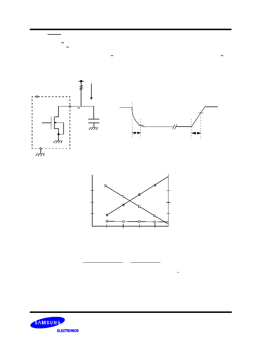
FLASH MEMORY
40
Advance
K9F4G08U0M
K9K8G08U1M
READY/BUSY
The device has a R/B output that provides a hardware method of indicating the completion of a page program, erase and random
read completion. The R/B pin is normally high but transitions to low after program or erase command is written to the command regis-
ter or random read is started after address loading. It returns to high when the internal controller has finished the operation. The pin is
an open-drain driver thereby allowing two or more R/B outputs to be Or-tied. Because pull-up resistor value is related to tr(R/B) and
current drain during busy(ibusy) , an appropriate value can be obtained with the following reference chart(Fig.20). Its value can be
determined by the following guidance.
V
CC
R/B
open drain output
Device
GND
Rp
t
r
,
t
f [s
]
Ibusy [A]
Rp(ohm)
Figure 20. Rp vs tr ,tf & Rp vs ibusy
Ibusy
tr
ibusy
Busy
Ready Vcc
@ Vcc = 3.3V, Ta = 25
∞C , C
L
= 50pF
VOH
tf
tr
1K
2K
3K
4K
50n
100n
150n
3m
2m
1m
50
tf
100
150
200
1.8
1.8
1.8
1.8
2.4
1.2
0.8
0.6
VOL
where I
L
is the sum of the input currents of all devices tied to the R/B pin.
Rp value guidance
Rp(max) is determined by maximum permissible limit of tr
Rp(min, 3.3V part) =
V
CC
(Max.) - V
OL
(Max.)
I
OL
+
I
L
=
3.2V
8mA
+
I
L
3.3V device - V
OL
: 0.4V, V
OH
: 2.4V
C
L
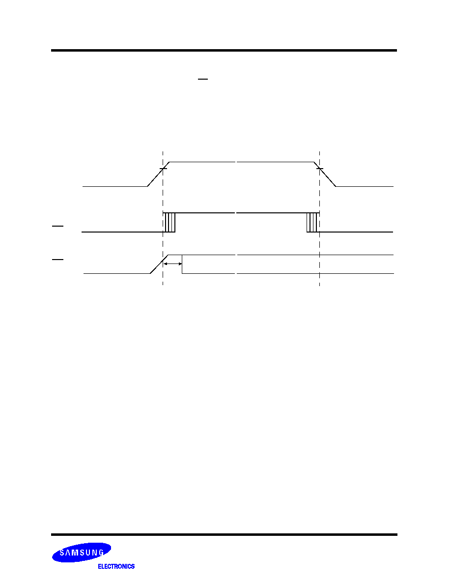
FLASH MEMORY
41
Advance
K9F4G08U0M
K9K8G08U1M
Data Protection & Power up sequence
The device is designed to offer protection from any involuntary program/erase during power-transitions. An internal voltage detector
disables all functions whenever Vcc is below about 2V. WP pin provides hardware protection and is recommended to be kept at V
IL
during power-up and power-down. A recovery time of minimum 10
µs is required before internal circuit gets ready for any command
sequences as shown in Figure 21. The two step command sequence for program/erase provides additional software protection.
Figure 21. AC Waveforms for Power Transition
V
CC
WP
High
WE
3.3V device : ~ 2.5V
3.3V device : ~ 2.5V
10
µs