Äîêóìåíòàöèÿ è îïèñàíèÿ www.docs.chipfind.ru

FLASH MEMORY
1
K9F5608D0D
K9F5608R0D
K9F5608U0D
K9F5608X0D
* Samsung Electronics reserves the right to change products or specification without notice.
INFORMATION IN THIS DOCUMENT IS PROVIDED IN RELATION TO SAMSUNG PRODUCTS,
AND IS SUBJECT TO CHANGE WITHOUT NOTICE.
NOTHING IN THIS DOCUMENT SHALL BE CONSTRUED AS GRANTING ANY LICENSE,
EXPRESS OR IMPLIED, BY ESTOPPEL OR OTHERWISE,
TO ANY INTELLECTUAL PROPERTY RIGHTS IN SAMSUNG PRODUCTS OR TECHNOLOGY. ALL
INFORMATION IN THIS DOCUMENT IS PROVIDED
ON AS "AS IS" BASIS WITHOUT GUARANTEE OR WARRANTY OF ANY KIND.
1. For updates or additional information about Samsung products, contact your nearest Samsung office.
2. Samsung products are not intended for use in life support, critical care, medical, safety equipment, or similar
applications where Product failure could result in loss of life or personal or physical harm, or any military or
defense application, or any governmental procurement to which special terms or provisions may apply.

FLASH MEMORY
2
K9F5608D0D
K9F5608R0D
K9F5608U0D
Document Title
32M x 8 Bit NAND Flash Memory
Revision History
The attached datasheets are prepared and approved by SAMSUNG Electronics. SAMSUNG Electronics CO., LTD. reserve the right
to change the specifications. SAMSUNG Electronics will evaluate and reply to your requests and questions about device. If you have
any questions, please contact the SAMSUNG branch office near you.
Revision No.
0.0
0.1
0.2
1.0
1.1
Remark
Advance
Advance
Preliminary
Final
History
Initial issue
1. Leaded package devices are eliminated
1. LOCKPRE pin mode is eliminated
Draft Date
May 16th. 2005
Aug. 11th. 2005
Oct. 17th. 2005
Oct. 30th. 2005
Dec. 30th 2005
Note : For more detailed features and specifications including FAQ, please refer to Samsung's Flash web site.
http://www.samsung.com/Products/Semiconductor/Flash/TechnicalInfo/datasheets.htm

FLASH MEMORY
3
K9F5608D0D
K9F5608R0D
K9F5608U0D
GENERAL DESCRIPTION
FEATURES
· Voltage Supply
- 1.8V device(K9F5608R0D) : 1.65~1.95V
- 2.65V device(K9F5608D0D) : 2.4~2.9V
- 3.3V device(K9F5608U0D) : 2.7 ~ 3.6 V
· Organization
- Memory Cell Array
-(32M + 1024K)bit x 8 bit
- Data Register
- (512 + 16)bit x 8bit
· Automatic Program and Erase
- Page Program
-(512 + 16)Byte
- Block Erase :
- (16K + 512)Byte
· Page Read Operation
- Page Size
- (512 + 16)Byte
- Random Access : 15
µs(Max.)
- Serial Page Access : 50ns(Min.)
· Fast Write Cycle Time
- Program time : 200
µs(Typ.)
- Block Erase Time : 2ms(Typ.)
32M x 8 Bit NAND Flash Memory
· Command/Address/Data Multiplexed I/O Port
· Hardware Data Protection
- Program/Erase Lockout During Power Transitions
· Reliable CMOS Floating-Gate Technology
- Endurance : 100K Program/Erase Cycles
- Data Retention : 10 Years
· Command Register Operation
· Intelligent Copy-Back
· Unique ID for Copyright Protection
· Package
- K9F5608D(U)0D-PCB0/PIB0
48 - Pin TSOP I (12 x 20 / 0.5 mm pitch)- Pb-free Package
- K9F5608X0D-JCB0/JIB0
63- Ball FBGA ( 9 x 11 /0.8mm pitch , Width 1.0 mm)
- Pb-free Package
- K9F5608U0D-FCB0/FIB0
48 - Pin WSOP I (12X17X0.7mm)- Pb-free Package
* K9F5608U0D-F(WSOPI ) is the same device as
K9F5608U0D-P(TSOP1) except package type.
Offered in 32Mx8bit , the K9F5608X0D is 256M bit with spare 8M bit capacity. The device is offered in 1.8V, 2.65V, 3.3V Vcc. Its
NAND cell provides the most cost-effective solutIon for the solid state mass storage market. A program operation can be performed
in typical 200
µs on a 528-byte page and an erase operation can be performed in typical 2ms on a 16K-byte block. Data in the page
can be read out at 50ns cycle time per byte. The I/O pins serve as the ports for address and data input/output as well as command
input. The on-chip write control automates all program and erase functions including pulse repetition, where required, and internal
verification and margining of data. Even the write-intensive systems can take advantage of the K9F5608X0D
s extended reliability of
100K program/erase cycles by providing ECC(Error Correcting Code) with real time mapping-out algorithm.
The K9F5608X0D is an optimum solution for large nonvolatile storage applications such as solid state file storage and other portable
applications requiring non-volatility.
PRODUCT LIST
Part Number
Vcc Range
Organization
PKG Type
K9F5608R0D-J
1.65 ~ 1.95V
X8
FBGA
K9F5608D0D-P
2.4 ~ 2.9V
TSOP1
K9F5608D0D-J
FBGA
K9F5608U0D-P
2.7 ~ 3.6V
TSOP1
K9F5608U0D-J
FBGA
K9F5608U0D-F
WSOP1
FLASH MEMORY
4
K9F5608D0D
K9F5608R0D
K9F5608U0D
PIN CONFIGURATION (TSOP1)
K9F5608D(U)0D-PCB0/PIB0
1
2
3
4
5
6
7
8
9
10
11
12
13
14
15
16
17
18
19
20
21
22
23
24
48
47
46
45
44
43
42
41
40
39
38
37
36
35
34
33
32
31
30
29
28
27
26
25
N.C
N.C
N.C
N.C
N.C
N.C
R/B
RE
CE
N.C
N.C
Vcc
Vss
N.C
N.C
CLE
ALE
WE
WP
N.C
N.C
N.C
N.C
N.C
N.C
N.C
N.C
N.C
I/O7
I/O6
I/O5
I/O4
N.C
N.C
N.C
Vcc
Vss
N.C
N.C
N.C
I/O3
I/O2
I/O1
I/O0
N.C
N.C
N.C
N.C
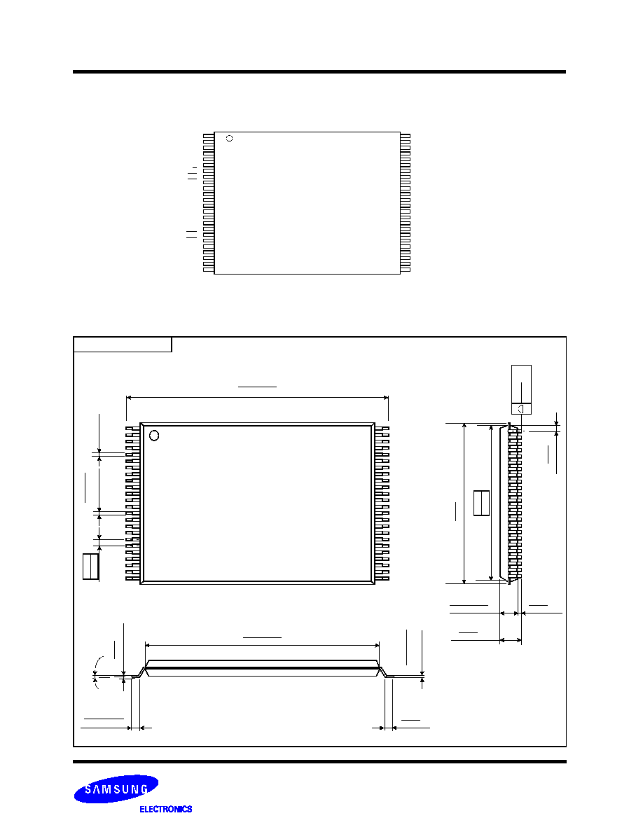
PACKAGE DIMENSIONS
48-PIN LEAD/LEAD FREE PLASTIC THIN SMALL OUT-LINE PACKAGE TYPE(I)
48 - TSOP1 - 1220F
Unit :mm/Inch
0.787
±0.008
20.00
±0.20
#1
#24
0.
16
+0
.
0
7
-0
.0
3
0.
008
+
0
.003
-0
.0
0
1
0.
50
0.0
197
#48
#25
0.
488
12.
40
MA
X
12.
00
0.
472
0.
10
0.0
04
MAX
0.
25
0.0
1
0
()
0.039
±0.002
1.00
±0.05
0.002
0.05
MIN
0.047
1.20
MAX
0.45~0.75
0.018~0.030
0.724
±0.004
18.40
±0.10
0~8
°
0.0
1
0
0.
25
TYP
0.
12
5
+0.0
75
0.035
0.
005
+0
.003
-
0
.001
0.50
0.020
(
)
0.
2
0
+0
.
0
7
-0
.0
3
FLASH MEMORY
5
K9F5608D0D
K9F5608R0D
K9F5608U0D
63-Ball FBGA (measured in millimeters)
PACKAGE DIMENSIONS
9.00
±0.10
#A1
Side View
Top View
1.0
0
(Max.)
0.45
±0.05
4
3
2
1
A
B
C
D
G
Bottom View
11
.
0
0
±
0.1
0
63-
0.45
±0.05
0.80 x7= 5.60
11
.
0
0
±
0.
1
0
0.80 x 5= 4.00
0.80
0.2
5
(Min.)
0.10MAX
B
A
2.80
2.00
9.00
±0.10
(Datum B)
(Datum A)
0.20
M
A B
0.80
0.80 x1
1=
8.8
0
0.80 x 9= 7.20
6
5
9.00
±0.10
E
F
H
K9F5608X0D-JCB0/JIB0
R/B
/WE
/CE
Vss
ALE
/WP
/RE
CLE
NC
NC
NC
NC Vcc
NC
NC I/O0
I/O1
NC
NC VccQ I/O5 I/O7
Vss
I/O6
I/O4
I/O3
I/O2
Vss
NC
NC
NC
NC
NC
NC
NC
NC
NC
NC
NC
NC
NC
NC
NC
NC
NC
NC
NC
NC
N.C
N.C N.C
N.C
N.C N.C
N.C
N.C
N.C N.C
N.C
N.C
N.C N.C
N.C
3
4
5
6
1 2
A
B
C
D
G
E
F
H
Top View
PIN CONFIGURATION (FBGA)
2.00
FLASH MEMORY
6
K9F5608D0D
K9F5608R0D
K9F5608U0D
PIN CONFIGURATION (WSOP1)
K9F5608U0D-FCB0/FIB0
1
2
3
4
5
6
7
8
9
10
11
12
13
14
15
16
17
18
19
20
21
22
23
24
48
47
46
45
44
43
42
41
40
39
38
37
36
35
34
33
32
31
30
29
28
27
26
25
N.C
N.C
DNU
N.C
N.C
N.C
R/B
RE
CE
DNU
N.C
Vcc
Vss
N.C
DNU
CLE
ALE
WE
WP
N.C
N.C
DNU
N.C
N.C
N.C
N.C
DNU
N.C
I/O7
I/O6
I/O5
I/O4
N.C
DNU
N.C
Vcc
Vss
N.C
DNU
N.C
I/O3
I/O2
I/O1
I/O0
N.C
DNU
N.C
N.C
PACKAGE DIMENSIONS
48-PIN LEAD PLASTIC VERY VERY THIN SMALL OUT-LINE PACKAGE TYPE (I)
48 - WSOP1 - 1217F
Unit :mm
15.40
±0.10
#1
#24
0.
20
+0
.
0
7
-0
.0
3
0.
16
+0
.07
-0
.0
3
0.
50TYP
(0
.
5
0
±
0.
0
6
)
#48
#25
0.
1
0
+0.0
75
-
0
.
035
17.00
±0.20
0°
~8
°
0.45~0.75
12.
00
±
0.1
0
0.58
±0.04
0.70 MAX
(0.01Min)
12.
40MA
X
FLASH MEMORY
7
K9F5608D0D
K9F5608R0D
K9F5608U0D
PIN DESCRIPTION
NOTE : Connect all V
CC
and V
SS
pins of each device to common power supply outputs.
Do not leave V
CC
or V
SS
disconnected.
Pin NAME
Pin Function
I/O
0
~ I/O
7
DATA INPUTS/OUTPUTS
The I/O pins are used to input command, address and data, and to output data during read operations. The I/
O pins float to high-z when the chip is deselected or when the outputs are disabled.
CLE
COMMAND LATCH ENABLE
The CLE input controls the activating path for commands sent to the command register. When active high,
commands are latched into the command register through the I/O ports on the rising edge of the WE signal.
ALE
ADDRESS LATCH ENABLE
The ALE input controls the activating path for address to the internal address registers. Addresses are
latched on the rising edge of WE with ALE high.
CE
CHIP ENABLE
The CE input is the device selection control. When the device is in the Busy state, CE high is ignored, and
the device does not return to standby mode in program or erase operation. Regarding CE control during
read operation, refer to 'Page read' section of Device operation.
RE
READ ENABLE
The RE input is the serial data-out control, and when active drives the data onto the I/O bus. Data is valid
tREA after the falling edge of RE which also increments the internal column address counter by one.
WE
WRITE ENABLE
The WE input controls writes to the I/O port. Commands, address and data are latched on the rising edge of
the WE pulse.
WP
WRITE PROTECT
The WP pin provides inadvertent write/erase protection during power tra nsitions. The internal high voltage
generator is reset when the WP pin is active low.
R/B
READY/BUSY OUTPUT
The R/B output indicates the status of the device operation. When low, it indicates that a program, erase or
random read operation is in process and returns to high state upon completion. It is an open drain output and
does not float to high-z condition when the chip is deselected or when outputs are disabled.
Vcc
Q
OUTPUT BUFFER POWER
Vcc
Q
is the power supply for Output Buffer.
Vcc
Q
is internally connected to Vcc, thus should be biased to Vcc.
Vcc
POWER
V
CC
is the power supply for device.
Vss
GROUND
N.C
NO CONNECTION
Lead is not internally connected.
DNU
DO NOT USE
Leave it disconnected
FLASH MEMORY
8
K9F5608D0D
K9F5608R0D
K9F5608U0D
512Byte
16 Byte
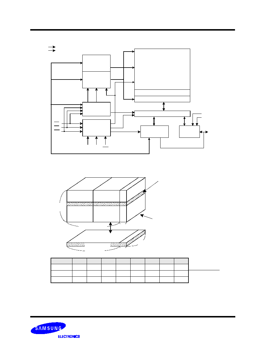
Figure 1-1. K9F5608X0D FUNCTIONAL BLOCK DIAGRAM
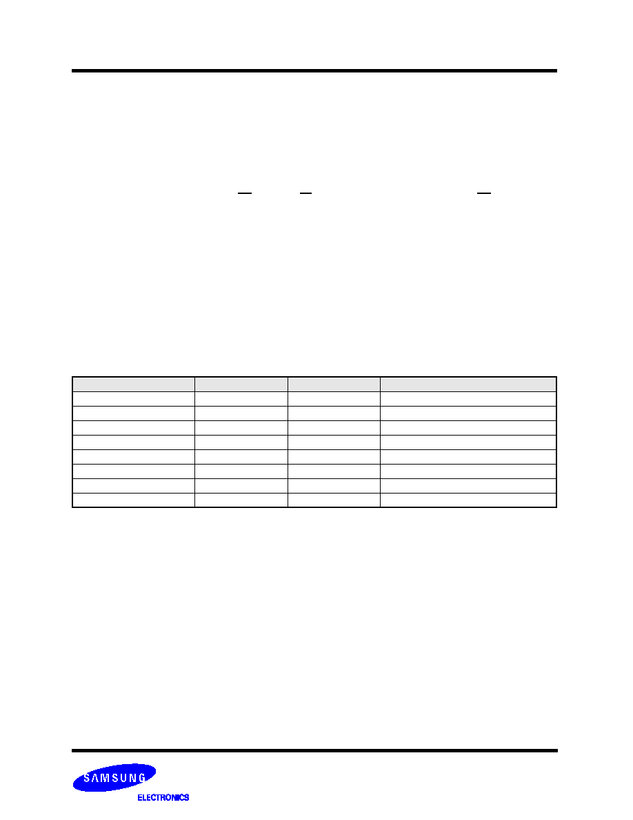
Figure 2-1. K9F5608X0D ARRAY ORGANIZATION
NOTE : Column Address : Starting Address of the Register.
00h Command(Read) : Defines the starting address of the 1st half of the register.
01h Command(Read) : Defines the starting address of the 2nd half of the register.
* A
8
is set to "Low" or "High" by the 00h or 01h Command.
* The device ignores any additional input of address cycles than required.
I/O 0
I/O 1
I/O 2
I/O 3
I/O 4
I/O 5
I/O 6
I/O 7
1st Cycle
A
0
A
1
A
2
A
3
A
4
A
5
A
6
A
7
2nd Cycle
A
9
A
10
A
11
A
12
A
13
A
14
A
15
A
16
3rd Cycle
A
17
A
18
A
19
A
20
A
21
A
22
A
23
A
24
V
CC
X-Buffers
256M + 8M Bit
Command
NAND Flash
ARRAY
(512 + 16)Byte x 65536
Y-Gating
Page Register & S/A
I/O Buffers & Latches
Latches
& Decoders
Y-Buffers
Latches
& Decoders
Register
Control Logic
& High Voltage
Generator
Global Buffers
Output
Driver
V
SS
A
9
- A
24
A
0
- A
7
Command
CE
RE
WE
WP
I/0 0
I/0 7
V
CC/
V
CCQ
V
SS
A
8
1st half Page Register
(=256 Bytes)
2nd half Page Register
(=256 Bytes)
64K Pages
(=2,048 Blocks)
512 Byte
8 bit
16 Byte
1 Block =32 Pages
= (16K + 512) Byte
I/O 0 ~ I/O 7
1 Page = 528 Byte
1 Block = 528 Byte x 32 Pages
= (16K + 512) Byte
1 Device = 528Bytes x 32Pages x 2048 Blocks
= 264 Mbits
Column Address
Row Address
(Page Address)
Page Register
CLE ALE
FLASH MEMORY
9
K9F5608D0D
K9F5608R0D
K9F5608U0D
PRODUCT INTRODUCTION
The K9F5608X0D is a 264Mbit(276,824,064 bit) memory organized as 65,536 rows(pages) by 528 columns. Spare eight columns are
located from column address of 512~527. A 528-byte data register is connected to memory cell arrays accommodating data transfer
between the I/O buffers and memory during page read and page program operations.The memory array is made up of 16 cells that
are serially connected to form a NAND structure. Each of the 16 cells resides in a different page. A block consists of two NAND struc-
tured strings. A NAND structure consists of 16 cells. Total 135168 NAND cells reside in a block. The array organization is shown in
Figure 2-1. The program and read operations are executed on a page basis, while the erase operation is executed on a block basis.
The memory array consists of 2048 separately erasable 16K-Byte blocks. It indicates that the bit by bit erase operation is prohibited
on the K9F5608X0D.
The K9F5608X0D has addresses multiplexed into 8 I/Os. This scheme dramatically reduces pin counts while providing high perfor-
mance and allows systems upgrades to future densities by maintaining consistency in system board design. Command, address and
data are all written through I/O
s by bringing WE to low while CE is low. Data is latched on the rising edge of WE. Command Latch
Enable(CLE) and Address Latch Enable(ALE) are used to multiplex command and address respectively, via the I/O pins. Some com-
mands require one bus cycle. For example, Reset command, Read command, Status Read command, etc require just one cycle bus.
Some other commands like Page Program and Copy-back Program and Block Erase, require two cycles: one cycle for setup and the
other cycle for execution. The 32M-byte physical space requires 24 addresses, thereby requiring three cycles for word-level address-
ing: column address, low row address and high row address, in that order. Page Read and Page Program need the same three
address cycles following the required command input. In Block Erase operation, however, only the two row address cycles are used.
Device operations are selected by writing specific commands into the command register. Table 1 defines the specific commands of
the K9F5608X0D.
The device includes one block sized OTP(One Time Programmable), which can be used to increase system security or to provide
identification capabilities. Detailed information can be obtained by contact with Samsung.
Table 1. COMMAND SETS
Caution : Any undefined command inputs are prohibited except for above command set of Table 1.
Function
1st. Cycle
2nd. Cycle
Acceptable Command during Busy
Read 1
00h/01h
-
Read 2
50h
-
Read ID
90h
-
Reset
FFh
-
O
Page Program
80h
10h
Copy-Back Program
00h
8Ah
Block Erase
60h
D0h
Read Status
70h
-
O
FLASH MEMORY
10
K9F5608D0D
K9F5608R0D
K9F5608U0D
RECOMMENDED OPERATING CONDITIONS
(Voltage reference to GND, K9F5608X0D-XCB0
:
T
A
=0 to 70
°C, K9F5608X0D-XIB0
:
T
A
=-40 to 85
°C)
Parameter
Symbol
K9F5608R0D(1.8V)
K9F5608D0D(2.65V)
K9F5608U0D(3.3V)
Unit
Min
Typ.
Max
Min
Typ.
Max
Min
Typ.
Max
Supply Voltage
V
CC
1.65
1.8
1.95
2.4
2.65
2.9
2.7
3.3
3.6
V
Supply Voltage
V
CCQ
1.65
1.8
1.95
2.4
2.65
2.9
2.7
3.3
3.6
V
Supply Voltage
V
SS
0
0
0
0
0
0
0
0
0
V
ABSOLUTE MAXIMUM RATINGS
NOTE :
1. Minimum DC voltage is -0.6V on input/output pins. During transitions, this level may undershoot to -2.0V for periods <30ns.
Maximum DC voltage on input/output pins is V
CC,
+0.3V which, during transitions, may overshoot to V
CC
+2.0V for periods <20ns.
2. Permanent device damage may occur if ABSOLUTE MAXIMUM RATINGS are exceeded. Functional operation should be restricted to the conditions
as detailed in the operational sections of this data sheet. Exposure to absolute maximum rating conditions for extended periods may affect reliability.
Parameter
Symbol
Rating
Unit
Voltage on any pin relative to V
SS
V
IN/OUT
-0.6 to + 4.6
V
V
CC
-0.6 to + 4.6
V
CCQ
-0.6 to + 4.6
Temperature Under Bias
K9F5608X0D-XCB0
T
BIAS
-10 to +125
°C
K9F5608X0D-XIB0
-40 to +125
Storage Temperature
K9F5608X0D-XCB0
T
STG
-65 to +150
°C
K9F5608X0D-XIB0
Short Circuit Current
Ios
5
mA
FLASH MEMORY
11
K9F5608D0D
K9F5608R0D
K9F5608U0D
DC AND OPERATING CHARACTERISTICS
(Recommended operating conditions otherwise noted.)
NOTE : V
IL
can undershoot to -0.4V and V
IH
can overshoot to V
CC
+0.4V for durations of 20 ns or less.
Parameter
Symbol
Test Conditions
K9F5608X0D
Unit
1.8V
2.65V
3.3V
Min Typ Max Min Typ Max Min Typ Max
Operat-
ing
Current
Sequential
Read
I
CC
1
tRC=50ns, CE=V
IL
I
OUT
=0mA
-
8
20
-
10
20
-
10
20
mA
Program
I
CC
2
-
-
8
20
-
10
20
-
10
25
Erase
I
CC
3
-
-
8
20
-
10
20
-
10
25
Stand-by Current(TTL)
I
SB
1 CE=V
IH
, WP=0V/V
CC
-
-
1
-
-
1
-
-
1
Stand-by Cur-
rent(CMOS)
I
SB
2 CE=V
CC
-0.2, WP=0V/V
CC
-
10
50
-
10
50
-
10
50
µA
Input Leakage Current
I
LI
V
IN
=0 to Vcc(max)
-
-
±10
-
-
±10
-
-
±10
Output Leakage Current
I
LO
V
OUT
=0 to Vcc(max)
-
-
±10
-
-
±10
-
-
±10
Input High Voltage
V
IH*
I/O pins
Vcc
Q
-0.4
-
V
CCQ
+0.3
V
CCQ
-0.4
-
V
CCQ
+0.3
2.0
-
V
CCQ
+0.3
V
Except I/O pins
V
CC
-0.4
-
V
CC
+0.3
V
CC
-0.4
-
V
CC
+0.3
2.0
-
V
CC
+0.3
Input Low Voltage, All
inputs
V
IL*
-
-0.3
-
0.4
-0.3
-
0.5
-0.3
-
0.8
Output High Voltage
Level
V
OH
K9F5608R0D :I
OH
=-100
µA
K9F5608D0D :I
OH
=-100
µA
K9F5608U0D :I
OH
=-400
µA
V
CCQ
-0.1
-
-
V
CCQ
-0.4
-
-
2.4
-
-
Output Low Voltage
Level
V
OL
K9F5608R0D :I
OL
=100uA
K9F5608D0D :I
OL
=100
µA
K9F5608U0D :I
OL
=2.1mA
-
-
0.1
-
-
0.4
-
-
0.4
Output Low Current(R/B) I
OL
(R/B)
K9F5608R0D :V
OL
=0.1V
K9F5608D0D :V
OL
=0.1V
K9F5608U0D :V
OL
=0.4V
3
4
-
3
4
-
8
10
-
mA
FLASH MEMORY
12
K9F5608D0D
K9F5608R0D
K9F5608U0D
CAPACITANCE
(
T
A
=25
°C, V
CC
=1.8V/2.65V/3.3V, f=1.0MHz)
NOTE : Capacitance is periodically sampled and not 100% tested.
Item
Symbol
Test Condition
Min
Max
Unit
Input/Output Capacitance
C
I/O
V
IL
=0V
-
10
pF
Input Capacitance
C
IN
V
IN
=0V
-
10
pF
VALID BLOCK
NOTE :
1. The
device
may include invalid blocks when first shipped. Additional invalid blocks may develop while being used. The number of valid blocks is pre-
sented with both cases of invalid blocks considered. Invalid blocks are defined as blocks that contain one or more bad bits
.
Do not erase or program
factory-marked bad blocks. Refer to the attached technical notes for a appropriate management of invalid blocks.
2. The 1st block, which is placed on 00h block address, is guaranteed to be a valid block, does not require Error Correction up to 1K Program/Erase
cycles.
3.
Minimum 1004 valid blocks are guaranteed for each contiguous 128Mb memory space.
Parameter
Symbol
Min
Typ.
Max
Unit
Valid Block Number
N
VB
2013
-
2048
Blocks
AC TEST CONDITION
(K9F5608X0D-XCB0 :TA=0 to 70
°C, K9F5608X0D-XIB0:TA=-40 to 85°C
K9F5608R0D : Vcc=1.65V~1.95V , K9F5608D0D : Vcc=2.4V~2.9V , K9F5608U0D : Vcc=2.7V~3.6V unless otherwise noted)
Parameter
K9F5608R0D
K9F5608D0D
K9F5608U0D
Input Pulse Levels
0V to Vcc
Q
0V to Vcc
Q
0.4V to 2.4V
Input Rise and Fall Times
5ns
5ns
5ns
Input and Output Timing Levels
Vcc
Q
/2
Vcc
Q
/2
1.5V
K9F5608R0D:Output Load (Vcc
Q
:1.8V +/-10%)
K9F5608D0D:Output Load (Vcc
Q
:2.65V +/-10%)
K9F5608U0D:Output Load (Vcc
Q
:3.0V +/-10%)
1 TTL GATE and CL=30pF 1 TTL GATE and CL=30pF 1 TTL GATE and CL=50pF
K9F5608U0D:Output Load (Vcc
Q
:3.3V +/-10%)
-
-
1 TTL GATE and CL=100pF
MODE SELECTION
NOTE : 1. X can be V
IL
or V
IH.
2. WP should be biased to CMOS high or CMOS low for standby.
CLE
ALE
CE
WE
RE
WP
Mode
H
L
L
H
X
Read Mode
Command Input
L
H
L
H
X
Address Input(3clock)
H
L
L
H
H
Write Mode
Command Input
L
H
L
H
H
Address Input(3clock)
L
L
L
H
H
Data Input
L
L
L
H
X
Data Output
L
L
L
H
H
X
During Read(Busy)
On K9F5608U0D_Y,P,V,F or K9F5608D0D_Y,P
X
X
X
X
H
X
During Read(Busy) on the devices except
On K9F5608U0D_Y,P,V,F or
K9F5608D0D_Y,P
X
X
X
X
X
H
During Program(Busy)
X
X
X
X
X
H
During Erase(Busy)
X
X
(1)
X
X
X
L
Write Protect
X
X
H
X
X
0V/V
CC
(2)
Stand-by
FLASH MEMORY
13
K9F5608D0D
K9F5608R0D
K9F5608U0D
PROGRAM/ERASE CHARACTERISTICS
Parameter
Symbol
Min
Typ
Max
Unit
Program Time
t
PROG
-
200
500
µs
Number of Partial Program Cycles
in the Same Page
Main Array
Nop
-
-
2
cycles
Spare Array
-
-
3
cycles
Block Erase Time
t
BERS
-
2
3
ms
AC TIMING CHARACTERISTICS FOR COMMAND / ADDRESS / DATA INPUT
NOTE: 1. If tCS is set less than 10ns, tWP must be minimum 35ns, otherwise, tWP may be minimum 25ns.
Parameter
Symbol
Min
Max
Unit
CLE setup Time
t
CLS
0
-
ns
CLE Hold Time
t
CLH
10
-
ns
CE setup Time
t
CS
0
-
ns
CE Hold Time
t
CH
10
-
ns
WE Pulse Width
t
WP
25
(1)
-
ns
ALE setup Time
t
ALS
0
-
ns
ALE Hold Time
t
ALH
10
-
ns
Data setup Time
t
DS
20
-
ns
Data Hold Time
t
DH
10
-
ns
Write Cycle Time
t
WC
50
-
ns
WE High Hold Time
t
WH
15
-
ns
Address to Data Loading Time
t
ADL
100
-
ns
FLASH MEMORY
14
K9F5608D0D
K9F5608R0D
K9F5608U0D
AC CHARACTERISTICS FOR OPERATION
NOTE: 1. K9F5608R0D tREA = 35ns.
2. If reset command(FFh) is written at Ready state, the device goes into Busy for maximum 5us.
3. The time to Ready depends on the value of the pull-up resistor tied R/B pin.
4. To break the sequential read cycle, CE must be held high for longer time than tCEH.
Parameter
Symbol
Min
Max
Unit
Data Transfer from Cell to Register
t
R
-
15
µs
ALE to RE Delay
t
AR
10
-
ns
CLE to RE Delay
t
CLR
10
-
ns
Ready to RE Low
t
RR
20
-
ns
RE Pulse Width
t
RP
25
-
ns
WE High to Busy
t
WB
-
100
ns
Read Cycle Time
t
RC
50
-
ns
RE Access Time
t
REA
-
30/35
(1)
ns
CE Access Time
t
CEA
-
45
ns
RE High to Output Hi-Z
t
RHZ
-
30
ns
CE High to Output Hi-Z
t
CHZ
-
20
ns
RE or CE High to Output hold
t
OH
15
-
ns
RE High Hold Time
t
REH
15
-
ns
Output Hi-Z to RE Low
t
IR
0
-
ns
WE High to RE Low
t
WHR
60
-
ns
Device Resetting Time
(Read/Program/Erase)
t
RST
-
5/10/500
(2)
µs
Symbol
Min
Max
Uni
K9F5608U0D-
P,F or
K9F5608D0D--
P only
Last RE High to Busy(at sequential read)
t
RB
-
100
ns
CE High to Ready(in case of interception by CE at
t
CRY
-
50 +tr(R/B)
(3)
ns
CE High Hold Time(at the last serial read)
(4)
t
CEH
100
-
ns
FLASH MEMORY
15
K9F5608D0D
K9F5608R0D
K9F5608U0D
NAND Flash Technical Notes
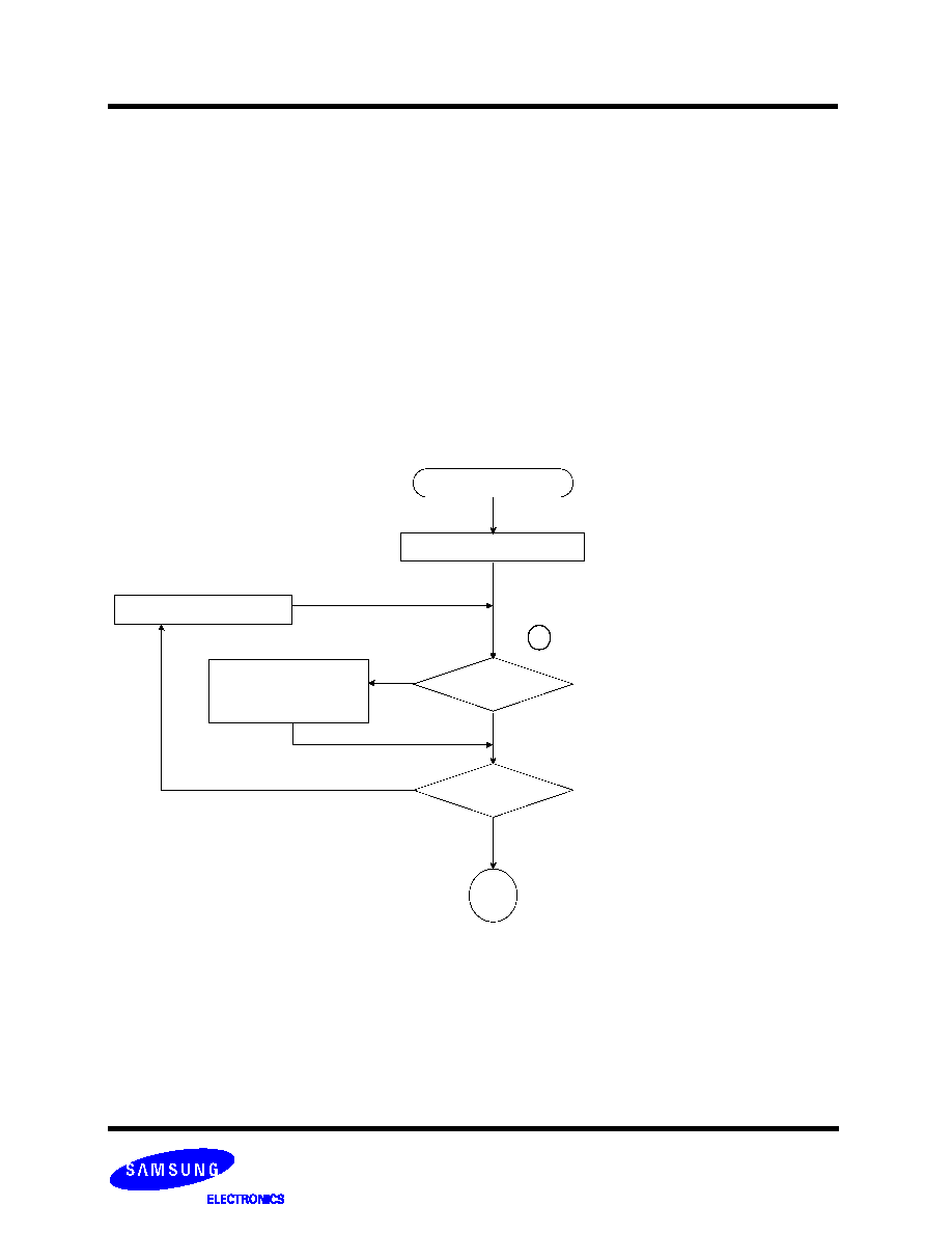
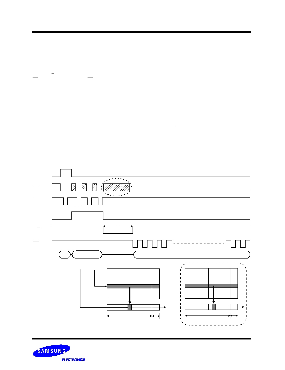
Identifying Initial Invalid Block(s)
Initial Invalid Block(s)
All device locations are erased(FFh) except locations where the initial invalid block(s) information is written prior to shipping. The
initial invalid block(s) status is defined by the 6th byte in the spare area. Samsung makes sure that either the 1st or 2nd page of every
initial invalid block has non-FFh data at the column address of 517. Since the initial invalid block information is also erasable in most
cases, it is impossible to recover the information once it has been erased. Therefore, the system must be able to recognize the initial
invalid block(s) based on the initial invalid block information and create the initial invalid block table via the following suggested flow
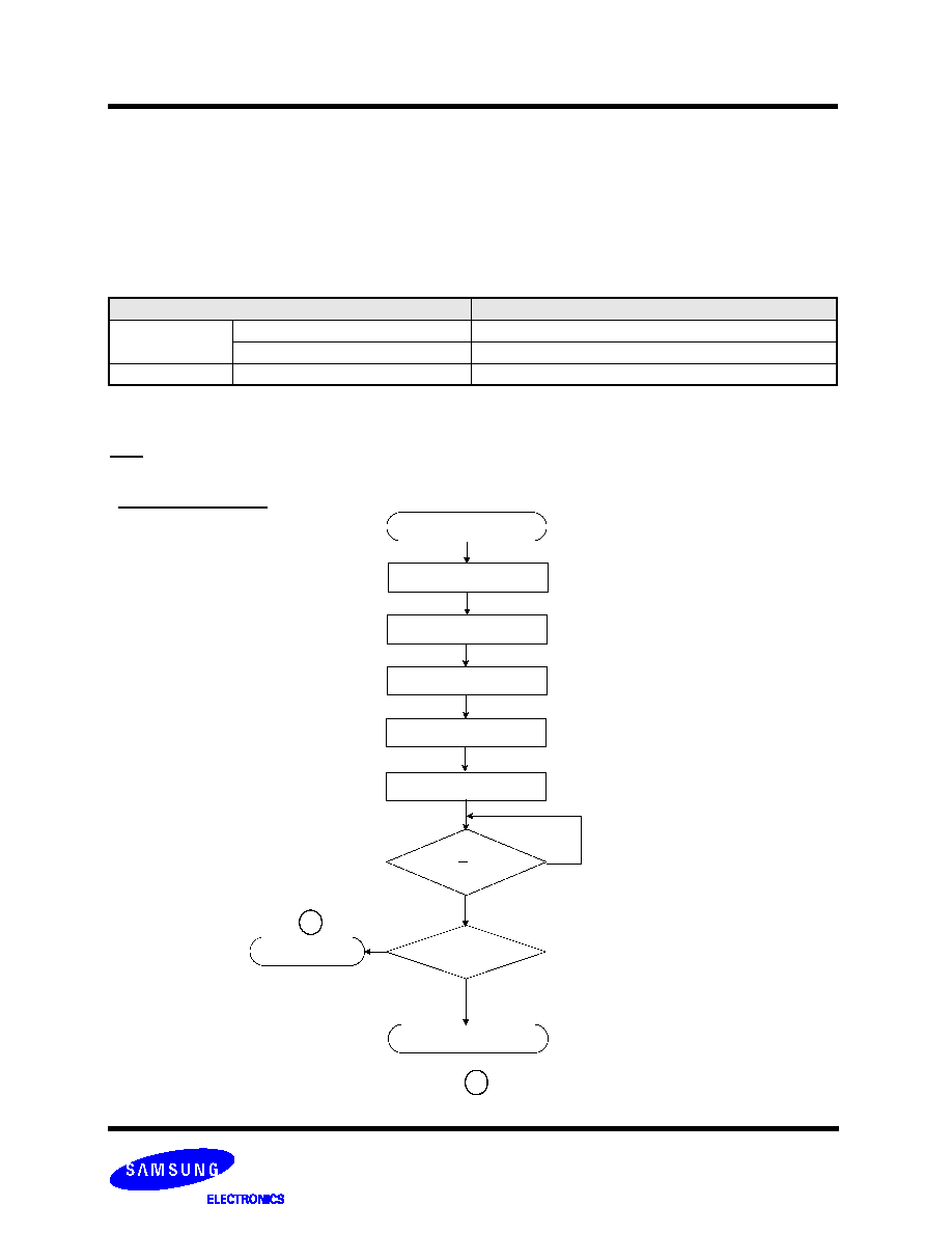
chart(Figure 3). Any intentional erasure of the initial invalid block information is prohibited.
*
Check "FFh" at the column address
Figure 3. Flow chart to create initial invalid block table.
Start
Set Block Address = 0
Check "FFh" ?
Increment Block Address
Last Block ?
End
No
Yes
Yes
Create (or update)
No
Initial
517of the 1st and 2nd page in the block
Invalid Block(s) Table
Initial invalid blocks are defined as blocks that contain one or more initial invalid bits whose reliability is not guaranteed by Samsung.
The information regarding the initial invalid block(s) is so called as the initial invalid block information. Devices with initial invalid
block(s) have the same quality level as devices with all valid blocks and have the same AC and DC characteristics. An initial invalid
block(s) does not affect the performance of valid block(s) because it is isolated from the bit line and the common source line by a
select transistor. The system design must be able to mask out the invalid block(s) via address mapping. The 1st block, which is
placed on 00h block address, is guaranteed to be a valid block, does not require Error Correction
up to 1K Program/Erase cycles.
FLASH MEMORY
16
K9F5608D0D
K9F5608R0D
K9F5608U0D
NAND Flash Technical Notes
(Continued)
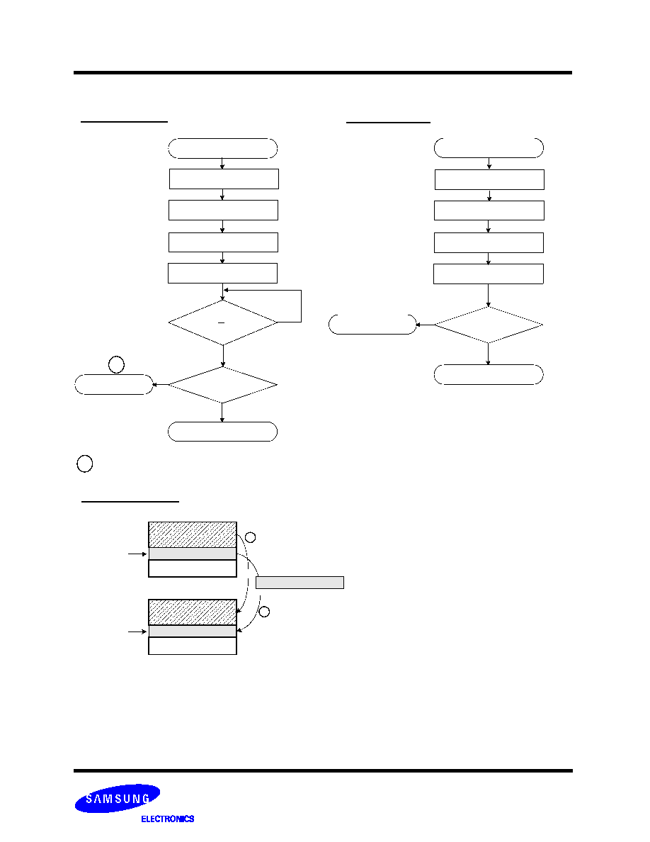
Program Flow Chart
Start
I/O 6 = 1 ?
I/O 0 = 0 ?
No
*
Write 80h
Write Address
Write Data
Write 10h
Read Status Register
Program Completed
or R/B = 1 ?
Program Error
Yes
No
Yes
Error in write or read operation
Within its life time, the additional invalid blocks may develop with NAND Flash memory. Refer to the qualification report for the actual
data.The following possible failure modes should be considered to implement a highly reliable system. In the case of status read fail-
ure after erase or program, block replacement should be done. Because program status fail during a page program does not affect
the data of the other pages in the same block, block replacement can be executed with a page-sized buffer by finding an erased
empty block and reprogramming the current target data and copying the rest of the replaced block. In case of Read, ECC must be
employed. To improve the efficiency of memory space, it is recommended that the read or verification failure due to single bit error be
reclaimed by ECC without any block replacement. The said additional block failure rate does not include those reclaimed blocks.
Failure Mode
Detection and Countermeasure sequence
Write
Erase Failure
Status Read after Erase --> Block Replacement
Program Failure
Status Read after Program --> Block Replacement
Read
Single Bit Failure
Verify ECC -> ECC Correction
ECC
: Error Correcting Code --> Hamming Code etc.
Example) 1bit correction & 2bit detection
: If program operation results in an error, map out
the block including the page in error and copy the
*
target data to another block.
FLASH MEMORY
17
K9F5608D0D
K9F5608R0D
K9F5608U0D
Erase Flow Chart
Start
I/O 6 = 1 ?
I/O 0 = 0 ?
No
*
Write 60h
Write Block Address
Write D0h
Read Status Register
or R/B = 1 ?
Erase Error
Yes
No
: If erase operation results in an error, map out
the failing block and replace it with another block.
*
Erase Completed
Yes
Read Flow Chart
Start
Verify ECC
No
Write 00h
Write Address
Read Data
ECC Generation
Reclaim the Error
Page Read Completed
Yes
NAND Flash Technical Notes
(Continued)
Block Replacement
* Step1
When an error happens in the nth page of the Block 'A' during erase or program operation.
* Step2
Copy the nth page data of the Block 'A' in the buffer memory to the nth page of another free block. (Block 'B')
* Step3
Then, copy the data in the 1st ~ (n-1)th page to the same location of the Block 'B'.
* Step4
Do not further erase Block 'A' by creating an 'invalid Block' table or other appropriate scheme.
Buffer memory of the controller.
1st
Block A
Block B
(n-1)th
nth
(page)
1
2
{
1st
(n-1)th
nth
(page)
{
an error occurs.
FLASH MEMORY
18
K9F5608D0D
K9F5608R0D
K9F5608U0D
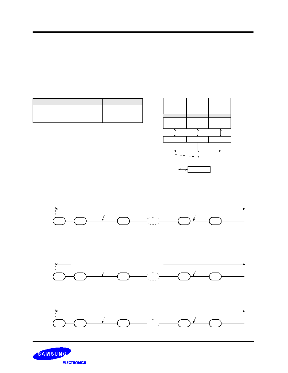
Samsung NAND Flash has three address pointer commands as a substitute for the two most significant column addresses. '00h'
command sets the pointer to 'A' area(0~255byte), '01h' command sets the pointer to 'B' area(256~511byte), and '50h' command sets
the pointer to 'C' area(512~527byte). With these commands, the starting column address can be set to any of a whole
page(0~527byte). '00h' or '50h' is sustained until another address pointer command is inputted. '01h' command, however, is effective
only for one operation. After any operation of Read, Program, Erase, Reset, Power_Up is executed once with '01h' command, the
address pointer returns to 'A' area by itself. To program data starting from 'A' or 'C' area, '00h' or '50h' command must be inputted
before '80h' command is written. A complete read operation prior to '80h' command is not necessary. To program data starting from
'B' area, '01h' command must be inputted right before '80h' command is written.
00h
(1) Command input sequence for programming 'A' area
Address / Data input
80h
10h
00h
80h
10h
Address / Data input
The address pointer is set to 'A' area(0~255), and sustained
01h
(2) Command input sequence for programming 'B' area
Address / Data input
80h
10h
01h
80h
10h
Address / Data input
'B', 'C' area can be programmed.
It depends on how many data are inputted.
'01h' command must be rewritten before
every program operation
The address pointer is set to 'B' area(256~512), and will be reset to
'A' area after every program operation is executed.
50h
(3) Command input sequence for programming 'C' area
Address / Data input
80h
10h
50h
80h
10h
Address / Data input
Only 'C' area can be programmed.
'50h' command can be omitted.
The address pointer is set to 'C' area(512~527), and sustained
'00h' command can be omitted.
It depends on how many data are inputted.
'A','B','C' area can be programmed.
Pointer Operation of K9F5608X0D(X8)
Table 2. Destination of the pointer
Command
Pointer position
Area
00h
01h
50h
0 ~ 255 byte
256 ~ 511 byte
512 ~ 527 byte
1st half array(A)
2nd half array(B)
spare array(C)
"A" area
256 Byte
(00h plane)
"B" area
(01h plane)
"C" area
(50h plane)
256 Byte
16 Byte
"A"
"B"
"C"
Internal
Page Register
Pointer select
commnad
(00h, 01h, 50h)
Pointer
Figure 4. Block Diagram of Pointer Operation
FLASH MEMORY
19
K9F5608D0D
K9F5608R0D
K9F5608U0D
System Interface Using CE don't-care.
CE
WE
t
WP
t
CH
t
CS
Start Add.(3Cycle)
80h
Data Input
CE
CLE
ALE
WE
Data Input
CE don't-care
10h
For an easier system interface, CE may be inactive during the data-loading or sequential data-reading as shown below. The internal
528byte page registers are utilized as seperate buffers for this operation and the system design gets more flexible. In addition, for
voice or audio applications which use slow cycle time on the order of u-seconds, de-activating CE during the data-loading and read-
ing would provide significant savings in power consumption.
Start Add.(3Cycle)
00h
CE
CLE
ALE
WE
Data Output(sequential)
CE don't-care
R/B
t
R
RE
t
CEA
out
t
REA
CE
RE
I/O
0
~
7
Figure 6. Program Operation with CE don't-care.
Figure 7. Read Operation with CE don't-care.
On K9F5608U0D_Y,P,V,F or K9F5608D0D_Y,P
I/Ox
I/Ox
CE must be held
low during tR
t
OH
FLASH MEMORY
20
K9F5608D0D
K9F5608R0D
K9F5608U0D
CE
WE
CLE
ALE
I/Ox
AO~A7
t
CLS
t
CS
t
WC
t
WP
t
ALS
t
DS
t
DH
t
ALH
t
ALS
t
WH
t
WC
t
WP
t
DS
t
DH
t
ALH
t
ALS
t
WH
t
WP
t
DS
t
DH
t
ALH
Command Latch Cycle
CE
WE
CLE
ALE
I/Ox
Command
Address Latch Cycle
t
CLS
t
CS
t
CLH
t
CH
t
WP
t
ALS
t
ALH
t
DS
t
DH
A17~A24
A9~A16
NOTE: 1. I/O8~15 must be set to "0" during command or address input.
I/O8~15 are used only for data bus.
Device
I/O
DATA
I/Ox
Data In/Out
K9F5608X0D(X8 device)
I/O 0 ~ I/O 7
~528byte
t
CH
FLASH MEMORY
21
K9F5608D0D
K9F5608R0D
K9F5608U0D
Input Data Latch Cycle
CE
CLE
WE
DIN 0
DIN 1
DIN n
ALE
t
ALS
t
CLH
t
WC
t
CH
t
DS
t
DH
t
DS
t
DH
t
DS
t
DH
t
WP
t
WH
t
WP
t
WP
Sequential Out Cycle after Read
(CLE=L, WE=H, ALE=L)
RE
CE
R/B
Dout
Dout
Dout
t
RC
t
REA
t
RR
t
OH
t
REA
t
REH
t
REA
t
OH
t
RHZ*
NOTES : Transition is measured
±200mV from steady state voltage with load.
This parameter is sampled and not 100% tested.
I/Ox
I/Ox
t
RHZ*
t
CHZ*
t
RP
FLASH MEMORY
22
K9F5608D0D
K9F5608R0D
K9F5608U0D
t
CHZ
t
OH
Status Read Cycle
CE
WE
CLE
RE
I/Ox
70h
Status Output
t
CLR
t
CLH
t
CS
t
WP
t
CH
t
DS
t
DH
t
REA
t
IR
t
OH
t
OH
t
WHR1
t
CEA
t
CLS
Read1 Operation
(Read One Page)
CE
CLE
R/B
WE
ALE
RE
Busy
Read
A0~A7
A9~A16
A17~A24
Dout N
Dout N+1 Dout N+2
Dout N+3
Column
Address
Page(Row)
Address
t
WB
t
AR
t
R
t
RC
t
RR
Dout m
t
WC
m = 528 , Read CMD = 00h or 01h
t
RHZ
t
CEH
t
RB
t
CRY
N Address
CMD
1)
1)
NOTES : 1) is only valid
On
K9F5608U0D_Y,P,V,F or K9F5608D0D_Y,P
I/Ox
On K9F5608U0D_Y,P,V,F or K9F5608D0D_Y,P
CE must be held
low during tR
t
RHZ
t
CHZ
t
OH
FLASH MEMORY
23
K9F5608D0D
K9F5608R0D
K9F5608U0D
Read1 Operation
(Intercepted by CE)
CE
CLE
R/B
WE
ALE
RE
Busy
Dout N
Dout N+1 Dout N+2
Dout N+3
Page(Row)
Address
Address
Column
t
WB
t
AR
t
CHZ
t
R
t
RR
t
RC
Read2 Operation
(Read One Page)
CE
CLE
R/B
WE
ALE
RE
50h
Dout
Dout n+m
M Address
n+M
Dout
n+M+1
Selected
Row
Start
address M
n
m
t
AR
t
R
t
WB
t
RR
A
0
~A
3
are Valid Address & A
4
~A
7
are Don
t
care
n = 512, m = 16
N Address
CMD
Read
I/Ox
I/Ox
Col. Add
Row Add1
Row Add2
Col. Add
Row Add1
Row Add2
On K9F5608U0D_Y,P,V,F or K9F5608D0D_Y,P
CE must be held
low during tR
On K9F5608U0D_Y,P,V,F or K9F5608D0D_Y,P
CE must be held
low during tR
t
OH
FLASH MEMORY
24
K9F5608D0D
K9F5608R0D
K9F5608U0D
Page Program Operation
CE
CLE
R/B
WE
ALE
RE
80h
70h
I/O
0
Din
N
Din
Din
10h
m
N+1
Sequential Data
Input Command
Column
Address
Page(Row)
Address
1 up to m Data
Serial Input
Program
Command
Read Status
Command
I/O
0
=0 Successful Program
I/O
0
=1 Error in Program
t
PROG
t
WB
t
WC
t
WC
t
WC
m = 528 byte
N Address
Sequential Row Read Operation
(only for
On K9F5608U0D_Y,P,V,F or K9F5608D0D_Y,P
)
CE
CLE
R/B
I/Ox
WE
ALE
RE
00h
M
Output
Dout
N
Dout
N+1
Dout
N+2
Dout
527
Dout
0
Dout
1
Dout
2
Dout
527
M+1
Output
N
Busy
Busy
Ready
I/Ox
Col. Add
Row Add1
Row Add2
Col. Add
Row Add1
Row Add2
t
ADL
FLASH MEMORY
25
K9F5608D0D
K9F5608R0D
K9F5608U0D
Block Erase Operation
(Erase One Block)
CE
CLE
R/B
WE
ALE
RE
60h
Auto Block Erase
Erase Command
Read Status
Command
I/O
0
=1 Error in Erase
D0h
70h
I/O 0
Busy
t
WB
t
BERS
I/O
0
=0 Successful Erase
Page(Row)
Address
t
WC
Setup Command
Copy-Back Program Operation
CE
CLE
R/B
WE
ALE
RE
00h
70h
I/O
0
8Ah
Column
Address
Page(Row)
Address
Program
Command
Read Status
Command
I/O
0
=0 Successful Program
I/O
0
=1 Error in Program
t
PROG
t
WB
t
WC
A
0
~A
7
A
17
~A
24
A
9
~A
16
Column
Address
Page(Row)
Address
Busy
t
WB
t
R
Busy
I/Ox
I/Ox
Col. Add Row Add1
Row Add2
A9~A16
A17~A24
FLASH MEMORY
26
K9F5608D0D
K9F5608R0D
K9F5608U0D
Manufacture & Device ID Read Operation
CE
CLE
WE
ALE
RE
90h
Read ID Command
Maker Code
Device Code
00h
t
REA
Address. 1cycle
t
AR
I/Ox
ECh
Device
Device
Device Code*
K9F5608R0D
35h
K9F5608D0D
75h
K9F5608U0D
75h
Code*
FLASH MEMORY
27
K9F5608D0D
K9F5608R0D
K9F5608U0D
DEVICE OPERATION
PAGE READ
Upon initial device power up, the device defaults to Read1 mode. This operation is also initiated by writing 00h to the command regis-
ter along with three address cycles. Once the command is latched, it does not need to be written for the following page read opera-
tion. Two types of operations are available : random read, serial page read.
The random read mode is enabled when the page address is changed. The 528 byte of data within the selected page are transferred
to the data registers in less than 15
µs(t
R
). The system controller can detect the completion of this data transfer(tR) by analyzing the
output of R/B pin. Once the data in a page is loaded into the registers, they may be read out in 50ns cycle time by sequentially pulsing
RE. High to low transitions of the RE clock output the data starting from the selected column address up to the last column address.
The way the Read1 and Read2 commands work is like a pointer set to either the main area or the spare area. Addresses A
0~
A
3
set
the starting address of the spare area while addresses A
4
~A
7
are ignored . The Read1 command is needed to move the pointer back
to the main area. Figures 8,9 show typical sequence and timings for each read operation.
Sequential Row Read is available only on
K9F5608U0D_Y,P,V,F or K9F5608D0D_Y,P
:
After the data of last column address is clocked out, the next page is automatically selected for sequential row read. Waiting 15
µs
again allows reading the selected page. The sequential row read operation is terminated by bringing CE high. Unless the operation
is aborted, the page address is automatically incremented for sequential row read as in Read1 operation and spare sixteen bytes of
each page may be sequentially read. The Sequential Read 1 and 2 operations are allowed only within a block and after the last page
of a block being readout, the sequential read operation must be terminated by bringing CE high. When the page address moves onto
the next block, read command and address must be given. Figures 8-1, 9-1 show typical sequence and timings for sequential row
read operation.
Figure8. Read1 Operation
Start Add.(3Cycle)
00h
A
0
~ A
7
& A
9
~ A
24
Data Output(Sequential)
(00h Command)
Data Field
Spare Field
CE
CLE
ALE
R/B
WE
RE
t
R
Main array
(01h Command)
Data Field
Spare Field
1st half array
2st half array
NOTE: 1) After data access on 2nd half array by 01h command, the start pointer is automatically moved to 1st half
array (00h) at next cycle.
I/Ox
On K9F5608U0D_Y,P,V,F or K9F5608D0D_Y,P
CE must be held
low during tR
1)
FLASH MEMORY
28
K9F5608D0D
K9F5608R0D
K9F5608U0D
Figure 9. Read2 Operation
50h
Data Output(Sequential)
Spare Field
CE
CLE
ALE
R/B
WE
Start Add.(3Cycle)
RE
t
R
Main array
Data Field
Spare Field
Figure 8-1. Sequential Row Read1 Operation
(only for
K9F5608U0D_Y,P,V,F or K9F5608D0D_Y,P
)
00h
01h
A
0
~ A
7
& A
9
~ A
24
I/Ox
R/B
Start Add.(3Cycle)
Data Output
Data Output
Data Output
1st
2nd
Nth
(528 Byte)
(528 Byte)
t
R
t
R
t
R
(00h Command)
Data Field
Spare Field
(01h Command)
Data Field
Spare Field
1st half array 2nd half array
1st
2nd
Nth
1st half array 2nd half array
1st
2nd
Nth
Block
A
4
~ A
7
Don't care
I/Ox
On K9F5608U0D_Y,P,V,F or K9F5608D0D_Y,P
CE must be held
low during tR
FLASH MEMORY
29
K9F5608D0D
K9F5608R0D
K9F5608U0D
Figure 9-1. Sequential Row Read2 Operation
(only for
K9F5608U0D_Y,P,V,F or K9F5608D0D_Y,P
)
50h
A
0
~ A
3
& A
9
~ A
24
I/Ox
R/B
Start Add.(3Cycle)
Data Output
Data Output
Data Output
2nd
Nth
(16Byte)
(16Byte)
Data Field
Spare Field
1st
Block
(A
4
~ A
7
:
Don
t Care)
1st
t
R
t
R
t
R
Nth
FLASH MEMORY
30
K9F5608D0D
K9F5608R0D
K9F5608U0D
PAGE PROGRAM
The device is programmed basically on a page basis, but it does allow multiple partial page programing of a byte/word or consecutive
bytes/words up to 528, in a single page program cycle. The number of consecutive partial page programming operation within the
same page without an intervening erase operation should not exceed 2 for main array and 3 for spare array. The addressing may be
done in any random order in a block. A page program cycle consists of a serial data loading period in which up to 528 bytes of data
may be loaded into the page register, followed by a non-volatile programming period where the loaded data is programmed into the
appropriate cell. About the pointer operation, please refer to the attached technical notes.
The serial data loading period begins by inputting the Serial Data Input command(80h), followed by the three cycle address input and
then serial data loading. The words other than those to be programmed do not need to be loaded.The Page Program confirm com-
mand(10h) initiates the programming process. Writing 10h alone without previously entering the serial data will not initiate the pro-
gramming process. The internal write controller automatically executes the algorithms and timings necessary for program and verify,
thereby freeing the system controller for other tasks. Once the program process starts, the Read Status Register command may be
entered, with RE and CE low, to read the status register. The system controller can detect the completion of a program cycle by mon-
itoring the R/B output, or the Status bit(I/O 6) of the Status Register. Only the Read Status command and Reset command are valid
while programming is in progress. When the Page Program is complete, the Write Status Bit(I/O 0) may be checked(Figure 10). The
internal write verify detects only errors for "1"s that are not successfully programmed to "0"s. The command register remains in Read
Status command mode until another valid command is written to the command register.
Figure 10. Program Operation
80h
R/B
Address & Data Input
I/O
0
Pass
10h
70h
Fail
t
PROG
COPY-BACK PROGRAM
The copy-back program is configured to quickly and efficiently rewrite data stored in one page within the array to another page within
the same array without utilizing an external memory. Since the time-consuming sequently-reading and its re-loading cycles are
removed, the system performance is improved. The benefit is especially obvious when a portion of a block is updated and the rest of
the block also need to be copied to the newly assigned free block. The operation for performing a copy-back is a sequential execution
of page-read without burst-reading cycle and copying-program with the address of destination page. A normal read operation with
"00h" command with the address of the source page moves the whole 528bytes data into the internal buffer. As soon as the Flash
returns to Ready state, copy-back programming command "8Ah" may be given with three address cycles of target page followed. The
data stored in the internal buffer is then programmed directly into the memory cells of the destination page. Once the Copy-Back Pro-
gram is finished, any additional partial page programming into the copied pages is prohibited before erase. Since the memory array is
internally partitioned into two different planes, copy-back program is allowed only within the same memory plane. Thus, A14, the
plane address, of source and destination page address must be the same."When there is a program-failure at Copy-Back opera-
tion, error is reported by pass/fail status. But if the soure page has a bit error for charge loss, accumulated copy-back
operations could also accumulate bit errors. For this reason, two bit ECC is recommended for copy-back operation."
Figure 11. Copy-Back Program Operation
00h
R/B
Add.(3Cycles)
I/O
0
Pass
8Ah
70h
Fail
t
PROG
Add.(3Cycles)
t
R
Source Address
Destination Address
I/Ox
I/Ox
FLASH MEMORY
31
K9F5608D0D
K9F5608R0D
K9F5608U0D
Figure 12. Block Erase Operation
BLOCK ERASE
The Erase operation is done on a block basis. Block address loading is accomplished in two cycles initiated by an Erase Setup com-
mand(60h). Only address A
14
to A
24
is valid while A
9
to A
13
is ignored. The Erase Confirm command(D0h) following the block address
loading initiates the internal erasing process. This two-step sequence of setup followed by execution command ensures that memory
contents are not accidentally erased due to external noise conditions.
At the rising edge of WE after the erase confirm command input, the internal write controller handles erase and erase-verify. When the
erase operation is completed, the Write Status Bit(I/O 0) may be checked. Figure 12 details the sequence.
60h
Block Add. : A
9
~ A
24
R/B
Address Input(2Cycle)
I/O
0
Pass
D0h
70h
Fail
t
BERS
READ STATUS
The device contains a Status Register which may be read to find out whether program or erase operation is completed, and whether
the program or erase operation is completed successfully. After writing 70h command to the command register, a read cycle outputs
the content of the Status Register to the I/O pins on the falling edge of CE or RE, whichever occurs last. This two line control allows
the system to poll the progress of each device in multiple memory connections even when R/B pins are common-wired. RE or CE
does not need to be toggled for updated status. Refer to table 4 for specific Status Register definitions. The command register
remains in Status Read mode until further commands are issued to it. Therefore, if the status register is read during a random read
cycle, a read command(00h or 50h) should be given before sequential page read cycle.
Table4. Read Status Register Definition
I/O #
Status
Definition
I/O 0
Program / Erase
"0" : Successful Program / Erase
"1" : Error in Program / Erase
I/O 1
Reserved for Future
Use
"0"
I/O 2
"0"
I/O 3
"0"
I/O 4
"0"
I/O 5
"0"
I/O 6
Device Operation
"0" : Busy "1" : Ready
I/O 7
Write Protect
"0" : Protected "1" : Not Protected
I/Ox
FLASH MEMORY
32
K9F5608D0D
K9F5608R0D
K9F5608U0D
Figure 13. Read ID Operation
CE
CLE
ALE
RE
WE
90h
00h
Address. 1cycle
Maker code
Device code
t
CEA
t
AR
t
REA
READ ID
The device contains a product identification mode, initiated by writing 90h to the command register, followed by an address input of
00h. Two read cycles sequentially output the manufacture code(ECh), and the device code respectively. The command register
remains in Read ID mode until further commands are issued to it. Figure 13 shows the operation sequence.
t
WHR1
Figure 14. RESET Operation
RESET
The device offers a reset feature, executed by writing FFh to the command register. When the device is in Busy state during random
read, program or erase mode, the reset operation will abort these operations. The contents of memory cells being altered are no
longer valid, as the data will be partially programmed or erased. The command register is cleared to wait for the next command, and
the Status Register is cleared to value C0h when WP is high. Refer to table 5 for device status after reset operation. If the device is
already in reset state a new reset command will not be accepted by the command register. The R/B pin transitions to low for tRST
after the Reset command is written. Refer to Figure 14 below.
Table5. Device Status
After Power-up
After Reset
Operation Mode
Read 1
Waiting for next command
FFh
R/B
t
RST
ECh
Device
I/Ox
I/Ox
Code*
Device
Device Code*
K9F5608R0D
35h
K9F5608D0D
75h
K9F5608U0D
75h
FLASH MEMORY
33
K9F5608D0D
K9F5608R0D
K9F5608U0D
READY/BUSY
The device has a R/B output that provides a hardware method of indicating the completion of a page program, erase and random
read completion. The R/B pin is normally high but transitions to low after program or erase command is written to the command reg-
ister or random read is started after address loading. It returns to high when the internal controller has finished the operation. The pin
is an open-drain driver thereby allowing two or more R/B outputs to be Or-tied. Because pull-up resistor value is related to tr(R/B)
and current drain during busy(ibusy) , an appropriate value can be obtained with the following reference chart(Fig 15). Its value can
be determined by the following guidance.
V
CC
R/B
open drain output
Device
GND
Rp
Figure 15. Rp vs tr ,tf & Rp vs ibusy
ibusy
Busy
Ready Vcc
VOH
tf
tr
VOL
C
L
1.8V device - V
OL
: 0.1V, V
OH
: Vcc
Q
-0.1V
3.3V device - V
OL
: 0.4V, V
OH
: 2.4V
2.65V device - V
OL
: 0.4V, V
OH
: Vcc
Q
-0.4V

FLASH MEMORY
34
K9F5608D0D
K9F5608R0D
K9F5608U0D
tr
,t
f [s]
Ib
usy
[A
]
Rp(ohm)
Ibusy
tr
@ Vcc = 3.3V, Ta = 25
°C , C
L
= 100pF
1K
2K
3K
4K
100n
200n
300n
3m
2m
1m
100
tf
200
300
400
3.6
3.6
3.6
3.6
2.4
1.2
0.8
0.6
Rp(min, 1.8V part) =
V
CC
(Max.) - V
OL
(Max.)
I
OL
+
I
L
=
1.85V
3mA
+
I
L
where I
L
is the sum of the input currents of all devices tied to the R/B pin.
Rp value guidance
Rp(max) is determined by maximum permissible limit of tr
Rp(min, 3.3V part) =
V
CC
(Max.) - V
OL
(Max.)
I
OL
+
I
L
=
3.2V
8mA
+
I
L
tr
,t
f
[s
]
Ib
usy
[A
]
Rp(ohm)
Ibusy
tr
@ Vcc = 1.8V, Ta = 25
°C , C
L
= 30pF
1K
2K
3K
4K
100n
200n
300n
3m
2m
1m
30
tf
60
90
120
1.7
1.7
1.7
1.7
1.7
0.85
0.57
0.43
tr
,t
f [s
]
Ibu
sy [A
]
Rp(ohm)
Ibusy
tr
@ Vcc = 2.65V, Ta = 25
°C , C
L
= 30pF
1K
2K
3K
4K
100n
200n
300n
3m
2m
1m
30
tf
60
90
120
2.3
2.3
2.3
2.3
2.3
1.1
0.75
0.55
Rp(min, 2.65V part) =
V
CC
(Max.) - V
OL
(Max.)
I
OL
+
I
L
=
2.5V
3mA
+
I
L
FLASH MEMORY
35
K9F5608D0D
K9F5608R0D
K9F5608U0D
The device is designed to offer protection from any involuntary program/erase during power-transitions. An internal voltage detector
disables all functions whenever Vcc is below about 1.1V(1.8V device), 1.8V(2.65V device), 2V(3.3V device). WP pin provides hard-
ware protection and is recommended to be kept at V
IL
during power-up and power-down and recovery time of minimum 10
µs is
required before internal circuit gets ready for any command sequences as shown in Figure 16. The two step command sequence for
program/erase provides additional software protection.
Figure 16. AC Waveforms for Power Transition
V
CC
WP
High
1.8V device : ~ 1.5V
WE
Data Protection & Power up sequence
3.3V device : ~ 2.5V
1.8V device : ~ 1.5V
3.3V device : ~ 2.5V
10
µs
2.65V device : ~ 2.0V
2.65V device : ~ 2.0V