K9K1G08U0M
FLASH MEMORY
1
Document Title
128M x 8 Bit NAND Flash Memory
Revision History
The attached data sheets are prepared and approved by SAMSUNG Electronics. SAMSUNG Electronics CO., LTD. reserve the
right to change the specifications. SAMSUNG Electronics will evaluate and reply to your requests and questions about device. If you
have any questions, please contact the SAMSUNG branch office near your office.
Revision No
0.0
0.1
0.2
0.3
0.4
0.5
Remark
History
1. Initial issue
1.[Page 31] device code (76h) --> device code (79h)
1.Powerup sequence is added
: Recovery time of minimum 1
µ
s is required before internal circuit gets
ready for any command sequences
2. AC parameter tCLR(CLE to RE Delay, min 50ns) is added.
3. [Page28] Only address A
14
to A
25
is valid while A
9
to A
13
is ignored
--> Only address A
14
to A
26
is valid while A
9
to A
13
is ignored
(page 30)
A14 and A15 must be the same between source and target page
--> A14 , A15 and A26 must be the same between source and target page
New definition of the number of invalid blocks is added.
(
Minimum 1004 valid blocks are guaranteed for each contiguous 128Mb
memory space.
)
Note is added.
(VIL can undershoot to -0.4V and VIH can overshoot to VCC +0.4V for
durations of 20 ns or less.)
V
CC
WP
High
2.5V
2.5V
WE
1
µ
Draft Date
Apr. 7th 2001
Jul. 3rd 2001
Jul. 23th 2001
Sep. 13th 2001
Apr. 4th 2003
Jun. 4th 2003
Note : For more detailed features and specifications including FAQ, please refer to Samsung's Flash web site.
http://www.samsung.com/Products/Semiconductor/Flash/TechnicalInfo/datasheets.htm

K9K1G08U0M
FLASH MEMORY
2
128M x 8 Bit NAND Flash Memory
The K9K1G08U0M is a 128M(134,217,728)x8bit NAND Flash
Memory with a spare 4.096K(4,194,304)x8bit. Its NAND cell
provides the most cost-effective solution for the solid state
mass storage market. A program operation can be performed
in typical 200
µ
s on the 528-byte page and an erase operation
can be performed in typical 2ms on a 16K-byte block. Data in
the page can be read out at 50ns cycle time per byte. The I/O
pins serve as the ports for address and data input/output as
well as command inputs. The on-chip write controller auto-
mates all program and erase functions including pulse repeti-
tion, where required, and internal verification and margining of
data. Even the write-intensive systems can take advantage of
the K9K1G08U0M's extended reliability of 100K program/erase
cycles by providing ECC(Error Correcting Code) with real time
mapping-out algorithm. The K9K1G08U0M-YCB0/YIB0 is an
optimum solution for large nonvolatile storage applications such
as solid state file storage and other portable applications requir-
ing non-volatility.
GENERAL DESCRIPTION
FEATURES
∑
Voltage Supply : 2.7V~3.6V
∑
Organization
- Memory Cell Array : (128M + 4,096K)bit x 8bit
- Data Register : (512 + 16)bit x8bit multipled by eight planes
∑
Automatic Program and Erase
- Page Program : (512 + 16)Byte
- Block Erase : (16K + 512)Byte
∑
528-Byte Page Read Operation
- Random Access : 12
µ
s(Max.)
- Serial Page Access : 50ns(Min.)
∑
Fast Write Cycle Time
- Program time : 200
µ
s(Typ.)
- Block Erase Time : 2ms(Typ.)
∑
Command/Address/Data Multiplexed I/O Port
∑
Hardware Data Protection
- Program/Erase Lockout During Power Transitions
∑
Reliable CMOS Floating-Gate Technology
- Endurance : 100K Program/Erase Cycles
- Data Retention : 10 Years
∑
Command Register Operation
∑
Intelligent Copy-Back Operation
∑
Package :
- K9K1G08U0M-YCB0, K9K1G08U0M-YIB0 :
48 - Pin TSOP I (12 x 20 / 0.5 mm pitch)
∑
Simultaneous Four Page/Block Program/Erase
PIN CONFIGURATION
NOTE : Connect all V
CC
and V
SS
pins of each device to common power supply outputs.
Do not leave V
CC
or V
SS
disconnected.
48-pin TSOP1
Standard Type
12mm x 20mm
1
2
3
4
5
6
7
8
9
10
11
12
13
14
15
16
17
18
19
20
21
22
23
24
48
47
46
45
44
43
42
41
40
39
38
37
36
35
34
33
32
31
30
29
28
27
26
25
N.C
N.C
N.C
N.C
N.C
N.C
R/B
RE
CE
N.C
N.C
Vcc
Vss
N.C
N.C
CLE
ALE
WE
WP
N.C
N.C
N.C
N.C
N.C
N.C
N.C
N.C
N.C
I/O7
I/O6
I/O5
I/O4
N.C
N.C
N.C
Vcc
Vss
N.C
N.C
N.C
I/O3
I/O2
I/O1
I/O0
N.C
N.C
N.C
N.C
PIN DESCRIPTION
Pin Name
Pin Function
I/O
0
~ I/O
7
Data Input/Outputs
CLE
Command Latch Enable
ALE
Address Latch Enable
CE
Chip Enable
RE
Read Enable
WE
Write Enable
WP
Write Protect
R/B
Ready/Busy output
V
CC
Power(+2.7V~3.6V)
V
SS
Ground
N.C
No Connection

K9K1G08U0M
FLASH MEMORY
3
512B Bytes
16 Bytes
Figure 1. Functional Block Diagram
Figure 2. Array Organization
NOTE : Column Address : Starting Address of the Register.
00h Command(Read) : Defines the starting address of the 1st half of the register.
01h Command(Read) : Defines the starting address of the 2nd half of the register.
* A
8
is set to "Low" or "High" by the 00h or 01h Command.
* L must be set to "Low".
* The device ignores any additional input of address cycles than reguired.
I/O 0
I/O 1
I/O 2
I/O 3
I/O 4
I/O 5
I/O 6
I/O 7
1st Cycle
A
0
A
1
A
2
A
3
A
4
A
5
A
6
A
7
2nd Cycle
A
9
A
10
A
11
A
12
A
13
A
14
A
15
A
16
3rd Cycle
A
17
A
18
A
19
A
20
A
21
A
22
A
23
A
24
4th Cycle
A
25
A
26
*L
*L
*L
*L
*L
*L
V
CC
X-Buffers
Command
I/O Buffers & Latches
Latches
& Decoders
Y-Buffers
Latches
& Decoders
Register
Control Logic
& High Voltage
Generator
Global Buffers
Output
Driver
V
SS
A
9
- A
26
A
0
- A
7
Command
CE
RE
WE
CLE
WP
I/0 0
I/0 7
V
CC
V
SS
A
8
1st half Page Register
(=256 Bytes)
2nd half Page Register
(=256 Bytes)
256K Pages
(=8,192 Blocks)
512 Bytes
8 bit
16 Bytes
1 Block = 32 Pages
(16K + 512) Byte
I/O 0 ~ I/O 7
1 Page = 528 Bytes
1 Block = 528 B x 32 Pages
= (16K + 512) Bytes
1 Device = 528B x 32Pages x 8,192 Blocks
= 1,056 Mbits
Column Address
Row Address
(Page Address)
Page Register
ALE
1,024M + 32M Bit
NAND Flash
ARRAY
(512 + 16)Byte x 262,144
Y-Gating
Page Register & S/A
K9K1G08U0M
FLASH MEMORY
4
Product Introduction
The K9K1G08U0M is a 1,026Mbit(1,107,296,436 bit) memory organized as 262,144 rows(pages) by 528 columns. Spare sixteen col-
umns are located from column address of 512 to 527. A 528-byte data register is connected to memory cell arrays accommodating
data transfer between the I/O buffers and memory during page read and page program operations. The memory array is made up of
16 cells that are serially connected to form a NAND structure. Each of the 16 cells resides in a different page. A block consists of two
NAND structured strings. A NAND structure consists of 16 cells. Total 135168 NAND cells reside in a block. The array organization is
shown in Figure 2. The program and read operations are executed on a page basis, while the erase operation is executed on a block
basis. The memory array consists of 8,192 separately erasable 16K-byte blocks. It indicates that the bit by bit erase operation is pro-
hibited on the K9K1G08U0M.
The K9K1G08U0M has addresses multiplexed into 8 I/O's. This scheme dramatically reduces pin counts and allows systems
upgrades to future densities by maintaining consistency in system board design. Command, address and data are all written through
I/O's by bringing WE to low while CE is low. Data is latched on the rising edge of WE. Command Latch Enable(CLE) and Address
Latch Enable(ALE) are used to multiplex command and address respectively, via the I/O pins. The 128M byte physical space
requires 27 addresses, thereby requiring four cycles for byte-level addressing: column address, low row address and high row
address, in that order. Page Read and Page Program need the same four address cycles following the required command input. In
Block Erase operation, however, only the three row address cycles are used. Device operations are selected by writing specific com-
mands into the command register. Table 1 defines the specific commands of the K9K1G08U0M.
The device provides simultaneous program/erase capability up to four pages/blocks. By dividing the memory array into eight 128Mbit
separate planes, simultaneous multi-plane operation dramatically increases program/erase performance by 4X while still maintaining
the conventional 512 byte structure.
The extended pass/fail status for multi-plane program/erase allows system software to quickly identify the failing page/block out of
selected multiple pages/blocks. Usage of multi-plane operations will be described further throughout this document.
In addition to the enhanced architecture and interface, the device incorporates copy-back program feature from one page to another
of the same plane without the need for transporting the data to and from the external buffer memory. Since the time-consuming burst-
reading and data-input cycles are removed, system performance for solid-state disk application is significantly increased.
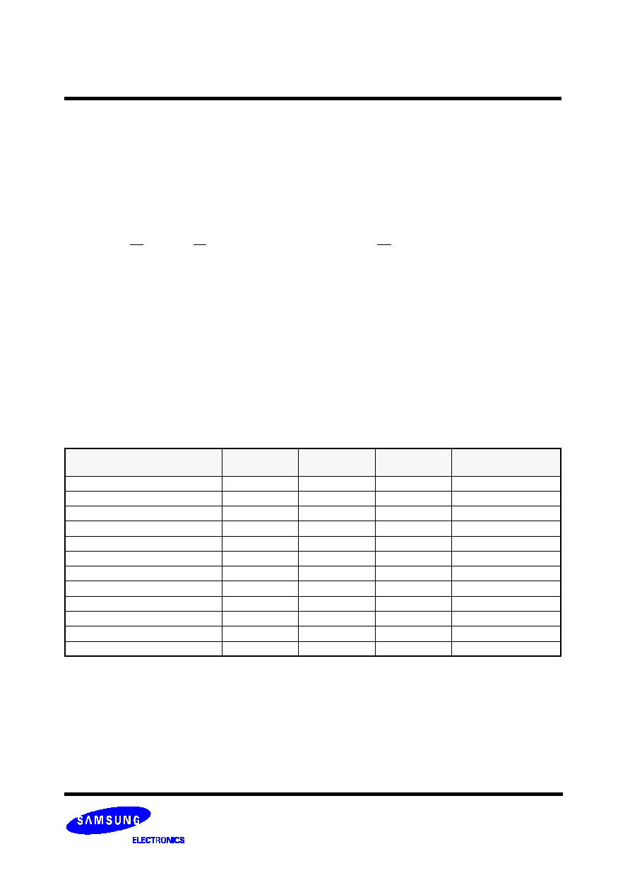
Table 1. Command Sets
NOTE : 1. The 00h command defines starting address of the 1st half of registers.
The 01h command defines starting address of the 2nd half of registers.
After data access on the 2nd half of register by the 01h command, the status pointer is
automatically moved to the 1st half register(00h) on the next cycle.
2. Page Program(True) and Copy-Back Program(True) are available on 1 plane operation.
Page Program(Dummy) and Copy-Back Program(Dummy) are available on the 2nd,3rd,4th plane of multi plane operation.
3. The 71h command should be used for read status of Multi Plane operation.
Caution : Any undefined command inputs are prohibited except for above command set of Table 1.
Function
1st. Cycle
2nd. Cycle
3rd. Cycle
Acceptable Command
during Busy
Read 1
00h/01h
(1)
-
-
Read 2
50h
-
-
Read ID
90h
-
-
Reset
FFh
-
-
O
Page Program (True)
(2)
80h
10h
-
Page Program (Dummy)
(2)
80h
11h
-
Copy-Back Program(True)
(2)
00h
8Ah
10h
Copy-Back Program(Dummy)
(2)
03h
8Ah
11h
Block Erase
60h
D0h
-
Multi-Plane Block Erase
60h----60h
D0h
-
Read Status
70h
-
-
O
Read Multi-Plane Status
71h
(3)
-
-
O

K9K1G08U0M
FLASH MEMORY
5
The device is arranged in eight 128Mbit memory planes. Each plane contains 1,024 blocks and 528 byte page registers. This allows
it to perform simultaneous page program and block erase by selecting one page or block from each plane. The block address map is
configured so that multi-plane program/erase operations can be executed for every four sequential blocks by dividing the memory
array into plane 0~3 or plane 4~7 separately. For example, multi-plane program/erase operations into plane 2,3,4 and 5 are prohib-
ited.
Plane 0
Plane 1
Plane 2
Plane 3
(1024 Block)
(1024 Block)
(1024 Block)
(1024 Block)
Page 0
Page 1
Page 31
Page 30
Memory Map
Block 0
Page 0
Page 1
Page 31
Page 30
Block 1
Page 0
Page 1
Page 31
Page 30
Block 2
Page 0
Page 1
Page 31
Page 30
Block 3
Page 0
Page 1
Page 31
Page 30
Block 4092
Page 0
Page 1
Page 31
Page 30
Block 4093
Page 0
Page 1
Page 31
Page 30
Block 4094
Page 0
Page 1
Page 31
Page 30
Block 4095
Page 0
Page 1
Page 31
Page 30
Block 4096
Page 0
Page 1
Page 31
Page 30
Block 4097
Page 0
Page 1
Page 31
Page 30
Block 4098
Page 0
Page 1
Page 31
Page 30
Block 4099
Page 0
Page 1
Page 31
Page 30
Block 8188
Page 0
Page 1
Page 31
Page 30
Block 8189
Page 0
Page 1
Page 31
Page 30
Block 8190
Page 0
Page 1
Page 31
Page 30
Block 8191
528byte Page Registers
Figure 3. Memory Array Map
528byte Page Registers
528byte Page Registers
528byte Page Registers
528byte Page Registers
528byte Page Registers
528byte Page Registers
528byte Page Registers
Plane 4
Plane 5
Plane 6
Plane 7
(1024 Block)
(1024 Block)
(1024 Block)
(1024 Block)