
SmartMedia
TM
1
K9S1208V0M/A-SSB0
K9D1G08V0M/A-SSB0
Document Title
64MB & 128MB SmartMedia
TM
Card
Revision History
The attached data sheets are prepared and approved by SAMSUNG Electronics. SAMSUNG Electronics CO., LTD. reserve the
right to change the specifications. SAMSUNG Electronics will evaluate and reply to your requests and questions about device. If you
have any questions, please contact the SAMSUNG branch office near your office.
Note : For more detailed features and specifications including FAQ, please refer to Samsung's Flash web site.
http://www.samsung.com/Products/Semiconductor/Flash/TechnicalInfo/datasheets.
Revision No
0.0
0.1
0.2
History
Initial issue
1. Changed DC characteristics
2. Added t
DBSY
parameter
3. Removed Copy-Back program command
4. Changed AC characteristics
1.Powerup sequence is added
Recovery time of minimum 1
�
s is required before internal circuit gets
ready for any command sequences
2. AC parameter tCLR(CLE to RE Delay, min 50ns) is added.
3. Changed AC characteristics
(Before)
Parameter
Min
Typ
Max
Unit
Operating
Current
Sequential Read
-
10
20->30
mA
Program
-
10
20->30
Erase
-
10
20->30
Parameter
Symbol
Min
Max
Unit
ALE to RE Delay
( ID read )
t
AR1
100->10
-
ns
Parameter
Symbol
Min
Max
Unit
ALE to RE Delay (ID read)
t
AR1
100
-
ns
ALE to RE Delay (Read
t
AR2
100
-
RE Low to Status Output
t
RSTO
-
35
CE Low to Status Output
t
CSTO
-
45
RE access time(Read ID)
t
READID
-
35
Draft Date
Mar. 30th 2001
Apr. 7th 2001
Sep. 7th 2001
Remark
Preliminary
V
CC
WP
High
~ 2.5V
~ 2.5V
WE
1
�
s
SmartMedia
TM
2
K9S1208V0M/A-SSB0
K9D1G08V0M/A-SSB0
Revision No
History
- AC characteristics (After)
. Deleted t
RSTO,
t
CSTO
and t
READID
/ Added
t
CLR,
t
CEA
Parameter
Symbol
Min
Max
Unit
ALE to RE Delay (ID read)
t
AR1
50
-
ns
ALE to RE Delay (Read cycle)
t
AR2
50
-
CLE to RE Delay
t
CLR
10
CE Access Time
t
CEA
-
45
Draft Date
Sep. 7th 2001
Remark
Final
Revision History
The attached data sheets are prepared and approved by SAMSUNG Electronics. SAMSUNG Electronics CO., LTD. reserve the
right to change the specifications. SAMSUNG Electronics will evaluate and reply to your requests and questions about device. If you
have any questions, please contact the SAMSUNG branch office near your office.
Note : For more detailed features and specifications including FAQ, please refer to Samsung Flash web site.
http://www.samsung.com/Products/Semiconductor/Flash/TechnicalInfo/datasheets.htm
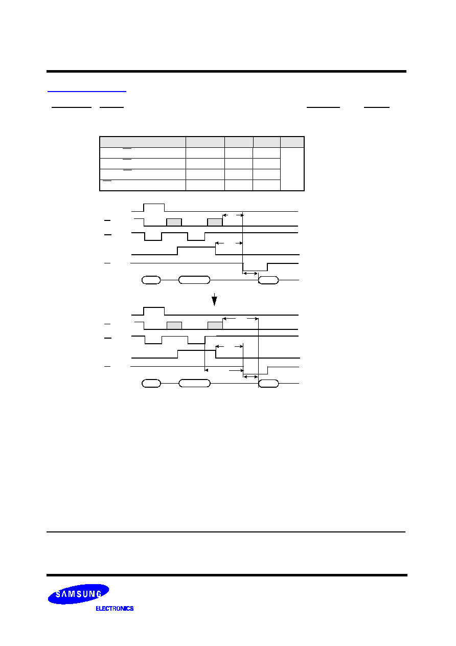
CE
CLE
I/O
0
~
7
ALE
RE
WE
90h
00h
ECh
Address. 1cycle
Maker code
tCEA
tAR
tREA
tWHR
CE
CLE
I/O
0
~
7
ALE
RE
WE
90h
00h
ECh
Address. 1cycle
Maker code
tCR
tAR
tREA

SmartMedia
TM
3
K9S1208V0M/A-SSB0
K9D1G08V0M/A-SSB0
History
1. Eliminated the duplicated AC parameter.
- AC characteristics (Before)
. Replaced t
AR1,
t
AR2
with t
AR
- AC characteristics (After)
Parameter
Symbol
Min
Max
Unit
ALE to RE Delay (ID read)
t
AR1
50
-
ns
ALE to RE Delay (Read cycle)
t
AR2
50
-
CLE to RE Delay
t
CLR
10
CE Access Time
t
CEA
-
45
Parameter
Symbol
Min
Max
Unit
ALE to RE Delay
t
AR
10
-
ns
CLE to RE Delay
t
CLR
10
CE Access Time
t
CEA
-
45
The attached data sheets are prepared and approved by SAMSUNG Electronics. SAMSUNG Electronics CO., LTD. reserve the
right to change the specifications. SAMSUNG Electronics will evaluate and reply to your requests and questions about device. If you
have any questions, please contact the SAMSUNG branch office near your office.
Revision History
Revision No
0.3
Remark
Final
Draft Date
Feb. 9th 2002
CE
WE
CLE
RE
I/O
0
~
7
70h
Status Output
tCLS
tCLH
tCS
tWP
tCH
tDS
tDH
tRSTO
tIR
tRHZ
tCHZ
tWHR
tCSTO
tCLS
CE
WE
CLE
RE
I/O
0
~
7
70h
Status Output
tCLS
tCLH
tCS
tWP
tCH
tDS
tDH
tREA
tIR
tRHZ
tCHZ
tWHR
tCEA
tCLS

SmartMedia
TM
4
K9S1208V0M/A-SSB0
K9D1G08V0M/A-SSB0
64MB & 128MB SmartMedia
TM
Card
Using Nand flash memory, SmartMedia provides the most cost-
effective solution for the solid state mass storage market. A pro-
gram operation is implemented by the single page of 528 bytes
in typical 200
�
s and an erase operation is done by the single
block of 16K bytes in typical 2ms. Data in the page can be read
out at 50ns cycle time per byte. The I/O pins serve as the ports
for address and data input/output as well as command inputs.
The on-chip write controller automates all program and erase
functions including pulse repetition, where required, and inter-
nal verification and margining of data. Even the write-intensive
systems can take advantage of the K9D1G08V0X,
K9S1208V0X
s extended reliability of 100K program/erase
cycles by providing ECC(Error Correcting Code) with real time
mapping-out algorithm. SmartMedia is an optimum solution for
large nonvolatile storage applications such as solid state file
storage, digital voice recorder, digital still camera and other por-
table applications requiring non-volatility.
GENERAL DESCRIPTION
FEATURES
�Single 2.7V~3.6V Supply
�Organization
- Memory Cell Array :
- K9S1208V0X: (64M + 2,048K)bit x 8bit
- K9D1G08V0X: (128M + 4,096K)bit x 8bit
- Data Register : (512 + 16)bit x8bit
�Automatic Program and Erase
- Page Program : (512 + 16)Byte
* Multi Page Program : 2K Bytes
- Block Erase : (16K + 512)Byte
�528-Byte Page Read Operation
- Random Access : 12
�
s(Max.)
- Serial Page Access : 50ns(Min.)
�Fast Write Cycle Time
- Program Time : 200
�
s(Typ.)
- Block Erase Time : 2ms(Typ.)
�Command/Address/Data Multiplexed I/O Port
�Hardware Data Protection
- Program/Erase Lockout During Power Transitions
�Reliable CMOS Floating-Gate Technology
- Endurance : 100K Program/Erase Cycles
- Data Retention : 10 Years
�Command Register Operation
�22pad SmartMedia
TM
(SSFDC)
�Unique ID for Copyright Protection
SmartMedia
TM
CARD(SSFDC)
Pin Name
Pin Function
I/O0 ~ I/O7
Data Input/Outputs
CLE
Command Latch Enable
ALE
Address Latch Enable
CE
Chip Enable
RE
Read Enable
WE
Write Enable
WP
Write Protect
LVD
Low Voltage Detect
GND
Ground
R/B
Ready/Busy output
V
CC
Power
V
SS
Ground
N.C
No Connection
PIN DESCRIPTION
12
13
14
15
16
17
18
19
20
21
22
V
CC
I/O
4
I/O
5
I/O
6
I/O
7
LVD
GND
R/B
RE
CE
V
CC
11
10
9
8
7
6
5
4
3
2
1
V
SS
V
SS
I/O
3
I/O
2
I/O
1
I/O
0
WP
WE
ALE
CLE
V
SS
22 PAD SmartMedia
TM
12
22
11
1
ID 128MB
NOTE : Connect all V
CC
and V
SS
pins of each device to common power supply outputs and do not leave V
CC
or V
SS
disconnected.
The pin 17(LVD) is used to detect 5V or 3.3V product electrically. Please, refer to the SmartMedia Application note for detail.

SmartMedia
TM
5
K9S1208V0M/A-SSB0
K9D1G08V0M/A-SSB0
Figure 1. FUNCTIONAL BLOCK DIAGRAM
V
CC
X-Buffers
Command
I/O Buffers & Latches
Latches
& Decoders
Y-Buffers
Latches
& Decoders
Register
Control Logic
& High Voltage
Generator
Global Buffers
Output
Driver
V
SS
A
9
- A
26
A
0
- A
7
Command
CE
RE
WE
CLE
WP
I/0 0
I/0 7
V
CC
V
SS
A
8
ALE
K9D1G08V0X : 1,024M + 32M Bit
NAND Flash
ARRAY
K9D1G08V0X : (512+16)Byte x 262,144
Y-Gating
Page Register & S/A
A
25
: K9S1208V0X
A
26
: K9D1G08V0X
K9S1208V0X : 512M + 16M Bit
K9S1208V0X : (512+16)Byte x 131,072