 | –≠–ª–µ–∫—Ç—Ä–æ–Ω–Ω—ã–π –∫–æ–º–ø–æ–Ω–µ–Ω—Ç: KB8825 | –°–∫–∞—á–∞—Ç—å:  PDF PDF  ZIP ZIP |

1.1GHZ DUAL PLL
KB8825
1
Final version ( 99.4.30 )
INTRODUCTION
The KB8825 is a high performance dual frequency synthesizer with
two integrated high frequency pre-scalers for RF operation up to 1.1
GHz.
The KB8825 is composed of modulus pre-scalers providing 64 and
66, no dead-zone PFD, selectable charge pump current, selectable
power down mode circuits, lock detector output, and loop filter
'
s time
constant switch.
It is fabricated using the ASP5HB Bi-CMOS process and is available
16-TSSOP with surface mount plastic packaging. Serial data is trans-
ferred into the KB8825 via three-wire interface (CK, DATA, EN).
FEATURES
∑
Two systems for receiver and transmitter
∑
Very low operating current consumption: Icc = Typ. 5.5mA @ 3.0V
∑
Low operating power supply voltage : 2.2 ~ 5.5V ( 200MHz ~ 550MHz Operating )
2.7 ~ 3.6V ( 550MHz ~ 1.1GHz Operating )
∑
Modulus pre-scaler: 64 / 66
∑
No dead-zone PFD
∑
Colpitt type local oscillation
∑
Selectable charge pump current
∑
Selectable power down mode
∑
TSSOP 16-pin package (0.65 mm pitch)
ORDERING INFORMATION
+: New product
APPLICATIONS
∑
Cordless telephone systems
∑
Portable wireless communications (PCS)
∑
Wireless Local Area Networks (WLANs)
∑
Other wireless communication systems
Device
Package
Operating Temperature
+KB8825
16
-
TSSOP
-
0044
-
30
∞
C to + 85
∞
C
16
-
TSSOP
-
0044
KB8825
1.1GHZ DUAL PLL
2
Final version ( 99.4.30 )
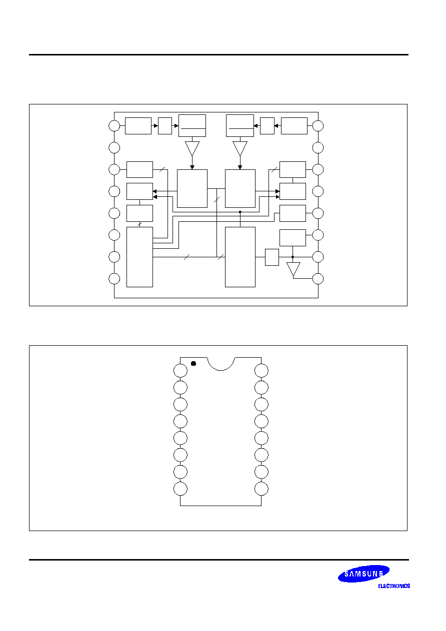
BLOCK DIAGRAM
PIN CONFIGURATION
Pre_Amp
1/2
Prescaler
1
32, 33
Buffer
1/2
Pre_Amp
16
15
Fin2
V
CC
OSCI
OSCO
1
2
3
4
5
6
7
8
Fin1
V
CC
CP1
GND
LD
CK
DATA
EN
Channel 2
Program-
able
Divider
14
13
12
11
10
9
Charge
Pump
Phase
Detector
Lock
Detector
Phase
Detector
Charge
Pump
Switch
Reference
Divider
Local
OSC
Control
Circuit
CP2
GND
SW
BO
Prescaler
1
32, 33
Channel 1
Program-
able
Divider
Buffer
Buffer
17
12
6
2
2
1/2
Fin1
V
CC
CP1
GND
LD
CK
DATA
EN
Fin2
V
CC
CP2
GND
SW
OSCI
OSCO
BO
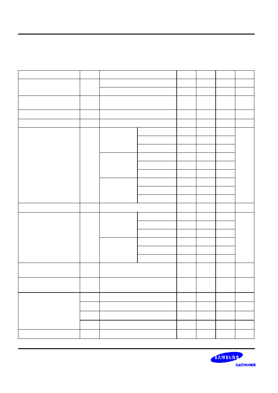
16TSSOP
KB8825
1
2
3
4
5
6
7
8
16
15
14
13
12
11
10
9

1.1GHZ DUAL PLL
KB8825
3
Final version ( 99.4.30 )
PIN DESCRIPTION
ABSOLUTE MAXIMUM RATINGS
Pin No.
Symbol
I/O
Description
1
Fin1
I
Input terminal of channel 1 RF signal.
2, 15
Vcc
-
Power supply voltage input. PIN2 and PIN15 are connected together.
3
CP1
O
Output terminal of channel 1 charge pump. Charge pump is constant current output
circuit, and output current is selected by input serial data.
4, 13
GND
-
Terminal of GND. PIN4 and PIN13 are connected in common.
5
LD
O
Output terminal of lock detection. It is the open drain output.
6
CK
I
Input terminal of clock.
7
DATA
I
Input terminal of data.
8
EN
I
Input terminal of enable signal.
9
BO
O
Output terminal of buffer amplifier. The signal of local oscillation is output through the
buffer amplifier.
10
OSCO
O
Output terminal of local oscillation signal.
11
OSCI
I
Input terminal of local oscillation signal. In case of external input, connecting it to this
terminal.
12
SW
O
Switchover terminal for the time constant of loop filter. It is an open drain output. If
you don
'
t switch the time constant of loop filter, general output is available.
14
CP2
0
Output terminal of channel 2 charge pump. Charge pump is a constant current output
circuit, and the output current is selected by input serial data.
16
Fin2
I
Input terminal of channel 2 RF signal.
Characteristic
Symbol
Value
Unit
Power Supply Voltage
Vcc
6
V
Power Dissipation
P
D
600
mW
Operating temperature
T
OPR
-
30 ~ + 85
∞
C
Storage temperature
T
STG
-
55~ +150
∞
C
Take care ! ESD sensitive device
KB8825
1.1GHZ DUAL PLL
4
Final version ( 99.4.30 )
ELECTRICAL CHARACTERISTICS
(Ta = 25
∞
C, V
CC
= 3V, unless otherwise specified)
Characteristic
Symbol
Test Conditions
Min.
Typ.
Max.
Unit
Operating Power supply
voltage
V
CC
Fin1=Fin2= 200MHz ~ 550MHz
2.2
3.0
5.5
V
Fin1=Fin2= 550MHz ~ 1.1GHz
2.7
3.0
3.6
V
Operating current
consumption
I
CC
Fin1=Fin2=1.1GHz/ -5dBm input
3.5
5.5
7.5
mA
Standby current
I
SB
Standby mode
-
0
10
µ
A
Fin operating frequency
Fin
Fin1 = Fin2 =
-
5dBm
200
-
1100
MHz
Fin input sensitivity
Fin
Fin1 = Fin2
= 200MHz
Vcc=2.2V
-
15
-
0
dBm
Vcc=3.0V
-
15
-
0
Vcc=5.5V
-
10
-
0
Fin1 = Fin2
= 550MHz
Vcc=2.2V
-
15
-
0
Vcc=3.0V
-
15
-
0
Vcc=5.5V
-
10
-
0
Fin1 = Fin2
= 1.1GHz
Vcc=2.7V
-
10
-
0
Vcc=3.0V
-
10
-
0
Vcc=3.6V
-
10
-
0
OSCI operating frequency
F
osc
V
Fin
= 0dBm, sinewave
5
-
25
MHz
OSCI input voltage
V
osc
f
osc
= 10MHz
Vcc=2.2V
-
10
0
5
dBm
Vcc=3.0V
-
10
0
5
Vcc=5.5V
0
-
5
f
osc
= 20MHz
Vcc=2.2V
-
10
0
5
Vcc=3.0V
-
10
0
5
Vcc=5.5V
-
5
0
5
Serial data input high
voltage (CK, DATA, EN)
V
IH
V
CC
= 2.2 to 5.5V
V
CC
-
0.4
-
-
V
Serial data input low voltage
(CK, DATA, EN)
V
IL
V
CC
= 2.2 to 5.5V
-
-
0.4
V
Charge pump output
current
I
CP1
CP1 = 0, CP2 = 0 VCP = 1.5 V
≠
±
100
-
µ
A
I
CP2
CP1 = 0, CP2 = 1 VCP = 1.5V
≠
±
200
-
µ
A
I
CP3
CP1 = 1, CP2 = 0 VCP = 1.5V
-
±
400
-
µ
A
I
CP4
CP1 = 1, CP2 = 1 VCP = 1.5V
-
±
800
-
µ
A
Charge pump leakage
I
CPL
Standby mode, Vcp = 1.5V
-1
-
+1
µ
A
1.1GHZ DUAL PLL
KB8825
5
Final version ( 99.4.30 )
FUNCTIONAL DESCRIPTIONS
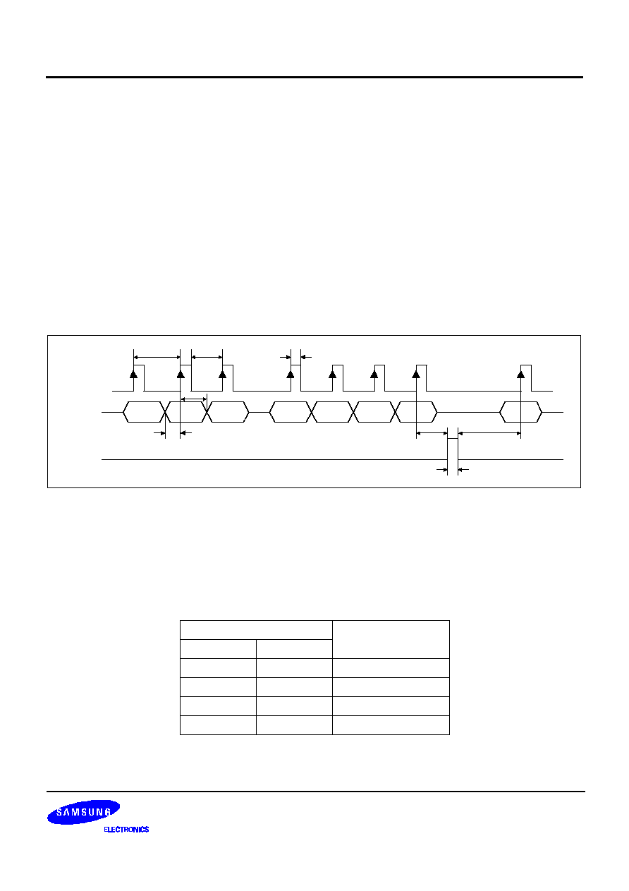
SERIAL DATA INPUT AND TIMING
CK (Pin6), DATA (Pin7), EN (Pin8) terminals in KB8825 are used for MICOM (MPU) serial data interface (MSB: 1st
input data; LSB: Last input data). Serial data controls the programmable reference divider, programmable divider
(CH1), programmable divider (CH2), and control latch separately by means of group code. Binary serial data is
entered via the DATA pin.
One bit of data is shifted into the internal shift register on the rising edge of the clock. When EN pin is high, stored
data is latched. The three terminals, CK, DATA, and EN, contain Schmitt trigger circuits to keep the data from
errors caused by noise, etc.
< Notice >
1. When power supply of KB8825 is disconnected, CLK, DATA, EN port from MCU should be pulled low.
2. When power goes up first, R counter data should be entered earlier than N1 and N2 counter data.
3. When power goes up first, control data should be entered earlier than N1 and N2 counter data.
Figure 1.
NOTE: Start data input with MSB first
SERIAL DATA GROUP AND GROUP CODE
The IC can be controlled through 4 kinds of group selection. Each group is identified by selective a 2-bit group code
given below.
Serial Bits
Group Location
GC1 (LSB)
GC2 (LSB-1)
0
0
Control Latch
0
1
Ch 1 N Latch
1
0
Ch 2 N Latch
1
1
OSC R Latch
1us
0.2us
0.2us
0.1us
0.2us
0.1us
0.2us
0.2us
EN
DATA
CK
MSB
N1 (R1)
N2 (R2)
N3 (R3)
N16 (R11) N17 (R12)
GC2
GC1
LSB
MSB