KM23V64015BF
CMOS MASK ROM
Preliminary Information
64M-Bit (8Mx8 /4Mx16) CMOS MASK ROM
The KM23V64015BF is a fully static mask programmable ROM
fabricated using silicon gate CMOS process technology, and is
organized either as 8,388,608 x 8 bit(byte mode) or as 4,194,304
x 16 bit(word mode) depending on BHE voltage level. This
device includes page read mode function, page read mode
allows 8 words (or 16 bytes) of data to be read fast in the same
page, CE and A
3
~ A
21
should not be changed.
This device operates with 3.0V or 3.3V power supply, and all
inputs and outputs are TTL compatible.
Because of its asynchronous operation, it requires no external
clock assuring extremely easy operation.
It is suitable for use in program memory of microprocessor, and
operating system and/or application software storage for hand-
held application.
The KM23V64015BF is packaged in a 48-CSP with 0.75mm ball
pitch and 6x8 ball array.
GENERAL DESCRIPTION
FEATURES
�
Switchable organization
8,388,608 x 8(byte mode)
4,194,304 x 16(word mode)
�
Fast access Time (C
L
=30pF)
Random Access Time/Page Access Time : 100/30ns(max.)
�
Supply voltage
V
CC
: single +3.3V/ single +3.0V
V
CCQ
: single +1.8V
�
8 words/16 bytes page access
�
Temperature : 0
�
C ~ +70
�
C
�
Current consumption
Operating(I
CC
) : 60mA (max)
Standby(I
SB2
) : 50uA (max)
�
Fully static operation
�
All inputs and outputs TTL compatible
�
Package
KM23V64015BF : 48-CSP with 0.75mm ball pitch
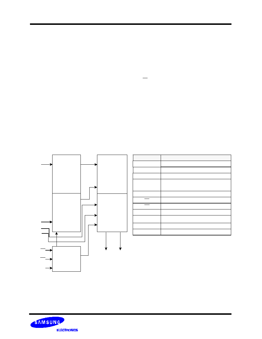
A
21
X
A
0~
A
2
AND
DECODER
BUFFERS
A
3
Y
AND
DECODER
BUFFERS
MEMORY CELL
SENSE AMP.
CONTROL
LOGIC
MATRIX
(4,194,304x16/
8,388,608x8)
DATA OUT
BUFFERS
A
-1
CE
OE
BHE
.
.
.
.
.
.
.
.
Q
0
/Q
8
Q
7
/Q
15
. . .
FUNCTIONAL BLOCK DIAGRAM
Pin Name
Pin Function
A
0
- A
2
Page Address Inputs
A
3
- A
21
Address Inputs
Q
0
- Q
14
Data Outputs
Q
15
/A
-1
Output 15(Word mode)/
LSB Address(Byte mode)
BHE
Word/Byte selection
CE
Chip Enable
OE
Output Enable
V
CC
Power
V
CCQ
Data Output Power (+1.8V)
V
SS
Ground
NC
No Connection
KM23V64015BF
CMOS MASK ROM
Preliminary Information
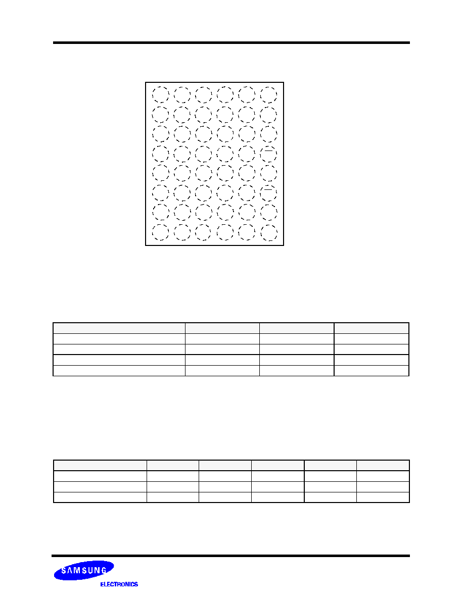
48FP-BGA PIN CONFIGURATION (TOP VIEW)
Note : See last page for package dimension.
ABSOLUTE MAXIMUM RATINGS
NOTE : Permanent device damage may occur if "ABSOLUTE MAXIMUM RATINGS" are exceeded. Functional operation should be
restricted to the conditions as detailed in the operational sections of this data sheet. Exposure to absolute maximum rating
conditions for extended periods may affect device reliability.
Item
Symbol
Rating
Unit
Voltage on Any Pin Relative to V
SS
V
IN
-0.3 to +4.5
V
Temperature Under Bias
T
BIAS
-10 to +85
�
C
Storage Temperature
T
Stg
-55 to +150
�
C
Operating Temperature
T
A
0 to +70
�
C
RECOMMENDED OPERATING CONDITIONS
(Voltage reference to V
SS
, T
A
= 0 to 70
�
C)
Item
Symbol
Min
Typ
Max
Unit
Supply Voltage
V
CC
2.7/3.0
3.0/3.3
3.3/3.6
V
Supply Voltage
V
CCQ
1.6
1.8
2.0
V
Supply Voltage
V
SS
0
0
0
V
N.C* : will be MSB Address for the 128Mbit.
1
2
3
4
5
6
A
B
C
D
E
F
G
H
A14
A10
N.C
A20
A6
A2
A13
A11
A19
N.C
A7
A3
A15
A12
A8
A21
A5
A4
D15/
A9
A18
V
CCQ
A17
OE
Vss
D6
V
CC
D2
D9
BHE
D7
D5
D10
D0
CE
A16
D14
D12
D11
D8
A0
N.C*
D13
D4
D3
D1
A1
Vss
A-1
KM23V64015BF
CMOS MASK ROM
Preliminary Information
DC CHARACTERISTICS
NOTE : Minimum DC Voltage(V
IL
) is -0.3V an input pins. During transitions, this level may undershoot to -2.0V for periods <20ns.
Maximum DC voltage on input pins(V
IH
) is V
DD
+0.3V which, during transitions, may overshoot to V
DD
+2.0V for periods <20ns.
Parameter
Symbol
Test Conditions
Min
Max
Unit
Operating Current
I
CC
CE=OE=V
IL
, all outputs open
-
60
mA
Standby Cur-
rent
TTL Level
I
SB1
CE=V
IH
, all outputs open
-
500
uA
CMOS Level
I
SB2
CE=V
CC
, all outputs open
-
50
uA
Input Leakage Current
I
LI
V
IN
=0 to V
CC
-
10
uA
Output Leakage Current
I
LO
V
OUT
=0 to V
CC
-
10
uA
Input High Voltage, All Inputs
V
IH
1.3
V
CC
+0.3
V
Input Low Voltage, All Inputs
V
IL
-0.3
0.5
V
Output High Voltage Level
V
OH
I
OH
= -200uA (V
CCQ
=1.8V)
1.4
-
V
Output Low Voltage Level
V
OL
I
OL
= 2.1mA
-
0.4
V
TEST CONDITIONS
Item
Value
Input Pulse Levels
GND to V
CCQ
Input Rise and Fall Times
3ns
Input Timing Reference Levels
V
CCQ
x 0.5V
Output timing Reference Levels
V
CCQ
x 0.5V
Output Loads
1 TTL Gate and C
L
=30pF
AC CHARACTERISTICS
(T
A
=0
�
C to +70
�
C, V
CC
=3.3V/3.0V
�
0.3V, V
CCQ
=1.8V
�
0.2V, unless otherwise noted.)
MODE SELECTION
CE
OE
BHE
Q
15
/A
-1
Mode
Data
Power
H
X
X
X
Standby
High-Z
Standby
L
H
X
X
Operating
High-Z
Active
L
L
H
Output
Operating
Q
0
~Q
15
: Dout
Active
L
Input
Operating
Q
0
~Q
7
: Dout
Q
8
~Q
14
: Hi-Z
Active
CAPACITANCE
( T
A
=25
�
C, f=1.0MHz)
NOTE : Capacitance is periodically sampled and not 100% tested.
Item
Symbol
Test Conditions
Min
Max
Unit
Output Capacitance
C
OUT
V
OUT
=0V
-
12
pF
Input Capacitance
C
IN
V
IN
=0V
-
12
pF
KM23V64015BF
CMOS MASK ROM
Preliminary Information
READ CYCLE (V
CCQ
=1.8V
�
0.2V
,
C
L
=30pF
)
NOTE : Page Address is determined as below.
Word mode (BHE=V
IH
) : A
0
, A
1,
A
2
Byte mode (BHE=V
IL
) : A
-1
, A
0
, A
1,
A
2
Item
Symbol
KM23V64015BF-10
Unit
Min
Max
Read Cycle Time
tRC
100
ns
Chip Enable Access Time
tACE
100
ns
Address Access Time
tAA
100
ns
Page Address Access Time
tPA
30
ns
Output Enable Access Time
tOE
30
ns
Output or Chip Disable to Output High-Z
tDF
20
ns
Output Hold from Address Change
tOH
0
ns
KM23V64015BF
CMOS MASK ROM
Preliminary Information
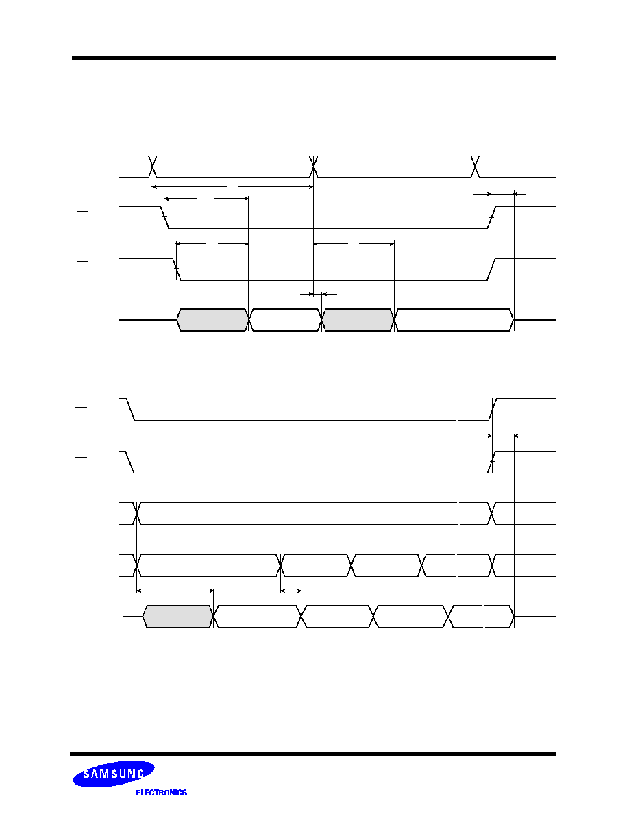
TIMING DIAGRAM
READ
ADD
CE
OE
D
OUT
A
0
~A
21
A
-1(*1)
D
0
~D
7
D
8
~D
15(*2)
PAGE READ
OE
ADD
D
OUT
CE
ADD
A
0,
A
1,
A
2
A
3
~A
21
VALID DATA
VALID DATA
VALID DATA
VALID DATA
1 st
2 nd
3 rd
t
DF(*3)
ADD1
ADD2
VALID DATA
VALID DATA
t
OH
t
DF(*3)
t
RC
t
ACE
t
OE
t
AA
NOTES :
*1.Byte Mode only. A
-1
is Least Significant Bit Address.(BHE = V
IL
)
*2. Word Mode only.(BHE = V
IH
)
*3. t
DF
is defined as the time at which the outputs achieve the open circuit condition and is not referenced to V
OH
or V
OL
level.
t
AA
t
PA
A
-1(*1)
D
0
~D
7
D
8
~D
15(*2)