
- 1 of 63 -
REV. 0.61 August 9. '99
128Mb DDR SDRAM
Target
DDR SDRAM Specification
Version 0.61
- 2 of 63 -
REV. 0.61 August 9. '99
128Mb DDR SDRAM
Target
Revision History
Version 0 (May, 1998)
- First version for internal review
Version 0.1(June, 1998)
- Added x4 organization
Version 0.2(Sep,1998)
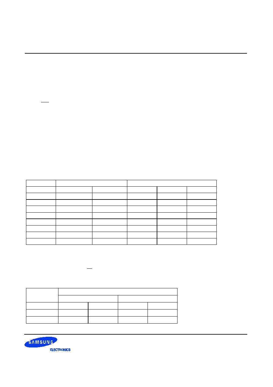
1. Added "Issue prcharge command for all banks of the device" as the fourth step of power-up squence.
2. In power down mode timing diagram, NOP condition is added to precharge power down exit.
Version 0.3(Dec,1998)
- Added QFC Function.
- Added DC current value
- Reduce I/O capacitance values
Version 0.4(Feb,1999)
-Added DDR SDRAM history for reference(refer to the following page)
-Added low power version DC spec
Version 0.5(Apr,1999)
-Revised following first showing for JEDEC standard
-Added DC target current based on new DC test condition
Version 0.6(July 1,1999)
1.Modified binning policy
From To
-Z (133Mhz) -Z (133Mhz/266Mbps@CL=2)
-8 (125Mhz) -Y (133Mhz/266Mbps@CL=2.5)
-0 (100Mhz) -0 (100Mhz/200Mbps@CL=2)
2.Modified the following AC spec values
*1
: Changed description method for the same functionality. This means no difference from the previous version.
3.Changed the following AC parameter symbol
From. To.
Output data access time from CK/CK tDQCK tAC
Version 0.61(August 9,1999)
- Changed the some values of "write with auto precharge" table for different bank in page 30.
From.
To.
-Z
-0
-Z
-Y
-0
tAC
+/- 0.75ns
+/- 1ns
+/- 0.75ns
+/- 0.75ns
+/- 0.8ns
tDQSCK
+/- 0.75ns
+/- 1ns
+/- 0.75ns
+/- 0.75ns
+/- 0.8ns
tDQSQ
+/- 0.5ns
+/- 0.75ns
+/- 0.5ns
+/- 0.5ns
+/- 0.6ns
tDS/tDH
0.5 ns
0.75 ns
0.5 ns
0.5 ns
0.6 ns
tCDLR
*1
2.5tCK-tDQSS
2.5tCK-tDQSS
1tCK
1tCK
1tCK
tPRE
*1
1tCK +/- 0.75ns
1tCK +/- 1ns
0.9/1.1 tCK
0.9/1.1 tCK
0.9/1.1 tCK
tRPST
*1
tCK/2 +/- 0.75ns
tCK/2 +/- 1ns
0.4/0.6 tCK
0.4/0.6 tCK
0.4/0.6 tCK
tHZQ
*1
tCK/2 +/- 0.75ns
tCK/2 +/- 1ns
+/- 0.75ns
+/- 0.75ns
+/-0.8ns
Asserted
command
For Different Bank
3
4
Old
New
Old
New
Read
Legal
Illegal
Legal
Illegal
Read + AP
*1
Legal
Illegal
Legal
Illegal

- 3 of 63 -
REV. 0.61 August 9. '99
128Mb DDR SDRAM
Target
Revision History
-
This revision history is for 64Mb and only for reference in other density.
Version 0.5 (JUN, 1997)
- First version for external release
- Center aligned DQ on reads and writes, 3.3V Vdd/Vddq, LVTTL for command and SSTL for DQ, DQS, CK and DM.
Version 0.6 (SEP. 1997)
- Changed to Edge alignedDQ on reads
- Add detailed discription for each functionality
Version 0.7 (JAN. 1998)
- Power supply: 3.3V +10%,-5% power supply for device operation (Vdd)
2.5V Power supply for I/O interface (Vddq)
- Interface: Add SSTL_2 for CK/DM (class I), DQ/DQS(class II) for KM416H431T.
* Put two part numbers, KM416H430T and KM416H431T.
- Clock input: Change to differential clock from single ended clock.
* Use CK, CK instead of CLK.
- Package: Change to 66pin TSOP-II, instead of 54pin TSOP-II
- tDQSS: Change to 0.75 ~ 1.25 tCK form 3ns ~ 1 tCK.
Add tSDQS(DQS-in setup time)
- In page 13, "DM can be ~" is modified to "DM must be ~".
- Tighten AC specs Change CK/CK hign/low level width from 0.4(min)/0.6(max)tCK to 0.45(min)/0.55(max)tCK.
-> Better input clock duty ratio from differential clock.
Version 0.8 (FEB. 1998)
- Correct pin rotation on pin 48 and 49 from 48-Vref, 49-Vss to 48-Vss, 49-Vref.
Version 0.9 (MAR. 1998)
- Change power-up sequence
. Add EMRS for DLL enable/disable
. Change DLL reset pin from A9 to A8 on MRS.
- Change speed range
. Add 133Mhz (266Mbps/pin), remove -12 (83Mhz)
- Change output load circuit
- Change input capacitance
- Add a comment on read interrupting write timing: Read command interrupting write can not be
issued at the next clock edge of write command.
- Modify the simplified state diagram on page 24.
Version 0.91 (May, 1998)
- Changed part number from KM416H430T/KM416H431T to KM416H4030T/KM416H4031T
- Added the 66pin package dimension on page 30.
- Changed Output Load Circuit 2 in page 29
- Removed CL=1.5
- Corrected typos

- 4 of 63 -
REV. 0.61 August 9. '99
128Mb DDR SDRAM
Target
Contents
Revision History
2
DDR SDRAM Ordering Information 8
1. Key Features
9
1.1 Features
9
1.2 Operating Frequencies
9
1.3 Device Information by organization 9
2. Package Pinout & Dimension
10
2.1 Package Pintout
10
2.2 Input/Output Function Description
11
2.3 66 Pin TSOP(II)/MS-024FC Package Physical Dimension
12
3. Functional Description
13
3.1 Simplified State Diagram
13
3.2 Basic Functionality
14
3.2.1 Power-Up Sequence
14
3.2.2 Mode Register Definition
15
3.2.2.1 Mode Register Set(MRS)
15
3.2.2.2 Extended Mode Register Set(EMRS)
17
3.2.3 Precharge
18
3.2.4 No Operation(NOP) & Device Deselect
18
3.2.5 Row Active
19
3.2.6 Read Bank
19
3.2.7 Write Bank
19
3.3 Essential Functionality for DDR SDRAM
20
3.3.1 Burst Read Operation
20
3.3.2 Burst Write Operation
21
3.3.3 Read Interrupted by a Read
22
3.3.4 Read Interrupted by a Write & Burst Stop
22
3.3.5 Read Interrupted by a Precharge
23
3.3.6 Write Interrupted by a Write
24

- 5 of 63 -
REV. 0.61 August 9. '99
128Mb DDR SDRAM
Target
3.3.7 Write Interrupted by a Read & DM
25
3.3.8 Write Interrupted by a Precharge & DM
26
3.3.9 Burst Stop
27
3.3.10 DM masking
28
3.3.11 Read With Auto Precharge
29
3.3.12 Write With Auto Precharge
30
3.3.13 Auto Refresh & Self Refresh
31
3.3.14 Power Down
32
4. Command Truth Table
33
5. Functional Truth Table
34
6. Absolute Maximum Rating
39
7. DC Operating Conditions & Specifications
39
7.1 DC Operating Conditions
39
7.2 DC Specifications 40
8. AC Operating Conditions & Timming Specification
41
8.1 AC Operating Conditions
41
8.2 AC Timming Parameters & Specification
42
9. AC Operating Test Conditions
44
10. Input/Output Capacitance
44
11. IBIS: I/V Characteristics for Input and Output Buffers
45
11.1 Normal strength driver 45
11.2 Half strength driver( will be included in the future) 47
12. QFC function
48
QFC definition
48
QFC timming on Read Operation
48
QFC timming on Write operation with tDQSSmax
49
QFC timming on Write operation with tDQSSmin
49

- 6 of 63 -
REV. 0.61 August 9. '99
128Mb DDR SDRAM
Target
Table 1 : Operating frequency and DLL jitter
Table 2. : Column address configurtion
Table 3 : Input/Output function description
Table 4 : Burst address ordering for burst length
Table 5 : Bank selection for precharge by bank address bits
Table 6 : Operating description when new command asserted while
read with auto precharge is issued
Table 7 : Operating description when new command asserted while
write with auto precharge is issued
Table 8 : Command truth table
Table 9-1 : Functional truth table
Table 9-2 : Functional truth table (contiued)
Table 9-3 : Functional truth table (contiued)
Table 9-4 : Functional truth table (contiued)
Table 9-5 : Functional truth table (cotinued)
Table 10 : Absolute maximum raings
Table 11 : DC operating condtion
Table 12 : DC specification
Table 13 : AC operating condition
Table 14 : AC timing parameters and specifications
Table 15 : AC operating test conditions
Table 16 : Input/Output capacitance
Table 17 : Pull down and pull up current values
List of tables
9
10
11
16
18
29
30
33
34
35
36
37
38
39
39
40
41
42
44
44
46

- 7 of 63 -
REV. 0.61 August 9. '99
128Mb DDR SDRAM
Target
Figure 1 : 128Mb Package Pinout
Figure 2 : Package dimension
Figure 3 :State digram
Figure 4 : Power up and initialization sequence
Figure 5 : Mode register set
Figure 6 : Mode register set sequence
Figure 7 : Extend mode register set
Figure 8 : Bank activation command cycle timing
Figure 9 : Burst read operation timing
Figure 10 : Burst write operation timing
Figure 11 : Read interrupted by a read timing
Figure 12 : Read interrupted by a write and burst stop timing
Figure 13 : Read interrupted by a precharge timing
Figure 14 : Write interrupted by a write timing
Figure 15 : Write interrupted by a read and DM timing
Figure 16 : Write interrupted by a precharge and DM timing
Figure 17 : Burst stop timing
Figure 18 : DM masking timing
Figure 19 : Read with auto precharge timing
Figure 20 : Write with auto precharge timing
Figure 21 : Auto refresh timing
Figure 22 : Self refresh timing
Figure 23 : Power down entry and exit timing
Figure 24 : Output Load Circuit (SSTL_2)
Figure 25 : I / V characteristics for input/output buffers:
pull-up(above) and pull-down(below)
Figure 26 : QFC timing on read operation
Figure 27 : QFC timing on write operation with tDQSSmax
Figure 28 : QFC timing on write operation with tDQSSmin
List of figures
10
12
13
14
15
16
17
19
20
21
22
22
23
24
25
26
27
28
29
30
31
31
32
44
45
48
49
49

- 8 of 63 -
REV. 0.61 August 9. '99
128Mb DDR SDRAM
Target
� 0 Mixed Interface(LVTTL & SSTL_3 & 3.3V V
DDQ
)
� 1 SSTL_2(2.5V V
DDQ
)
� T 66pin TSOP-II
� B BGA
� C u - BGA(CSP)
� Z 7.5ns, 133MHz@CL2 (266Mbps/pin)
� Y 7.5ns, 133MHz@CL2.5(266Mbps/pin)
� 0 10ns, 100MHz @CL2(200Mbps/pin)
� Blank 1st Gen.
� A 2nd Gen.
� B 3rd Gen.
� C 4th Gen.
� 4 4M
� 8 8M
� 16 16M
� 32 32M
� 64 64M
� 12 128M
� 25 256M
� 51 512M
� 1G 1G
� 2G 2G
� 4G 4G
� H DDR SDRAM(3.3V V
DD
)
� L DDR SDRAM(2.5V V
DD
)
� 4 x4
� 8 x8
� 16 x16
� 32 x32
� G Auto & Self Refresh
� F Auto & Self Refresh with Low Power
� 3 4 Banks
� 4 8 Banks
� 4 DRAM
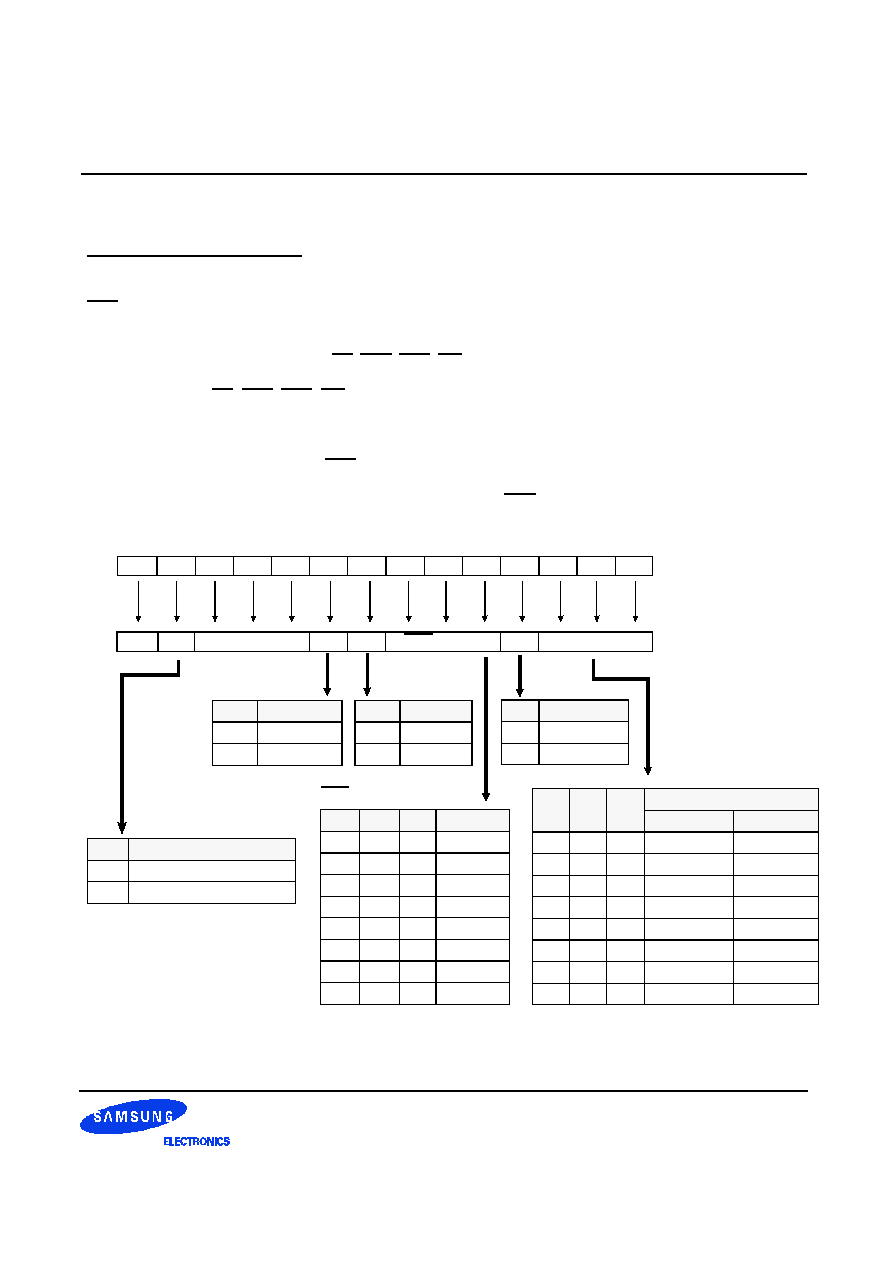
DDR SDRAM ORDERING INFORMATION
KM 4 XX L XX X X X X X - X X
1. SAMSUNG Memory
2. Device
3. Organization
4. Product & Voltage(V
DD
)
12. Speed
11. Power
10. Package Type
9. Revision
5. Depth
8. Interface & Voltage(V
DDQ
)
7. Number of Bank
1. SAMSUNG Memory
2. Device
3. Organization
4. Product & Voltage(V
DD
)
5. Depth
7. Number of Bank
8. Interface & Voltage(V
DDQ
)
9. Revision
10. Package Type
11. Power
12. Speed
6. Refresh
� 0 64m/4K(15.6us)
� 1 32m/2K(15.6us)
� 2 128m/8K(15.6us)
� 3 64m/8K(7.8us)
� 4 128m/16K(7.8us)
6. Refresh
- 9 of 63 -
REV. 0.61 August 9. '99
128Mb DDR SDRAM
Target
�
Double-data-rate architecture; two data transfers per clock cycle
� Bidirectional data strobe(DQS)
� Four banks operation
� Differential clock inputs(CK and CK)
� DLL aligns DQ and DQS transition with CK transition
� MRS cycle with address key programs
-. Read latency 2, 2.5 (clock)
-. Burst length (2, 4, 8)
-. Burst type (sequential & interleave)
� All inputs except data & DM are sampled at the positive going edge of the system clock(CK)
� Data I/O transactions on both edges of data strobe
� Edge aligned data output, center aligned data input
� LDM,UDM/DM for write masking only
� Auto & Self refresh
� 15.6us refresh interval
� Maximum burst refresh cycle : 8
� 66pin TSOP II package
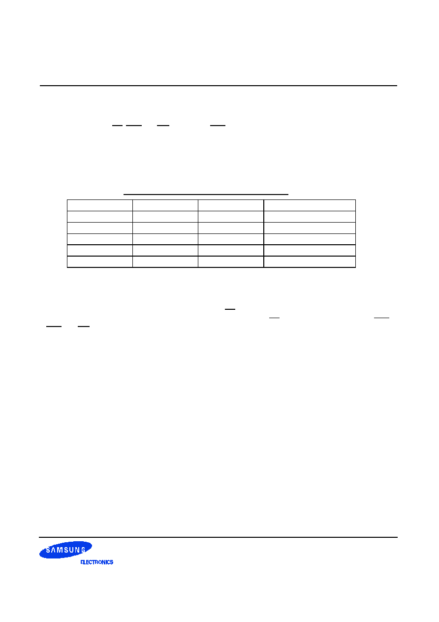
1. Key Features
1.1 Features
1.2 Operating Frequencies
PC266A(-Z)
PC266B(-Y)
PC200(-0)
Speed
133MHz@CL2
133MHz@CL2.5
100MHz@CL2
DLL jitter
�
0.75ns
�
0.75ns
�
0.8ns
*CL : Cas Latency
Maximum Operation
Frequency
Table 1. Operating frequency and DLL jitter
1.3 Device information by Organization
Density
Part No.
Operating Freq.
Interface
Package
128Mb
KM44L32031BT-G(F)Z/Y/0
133/133/100MHz
SSTL_2
66pin
TSOP II
KM48L16031BT-G(F)Z/Y/0
KM416L8031BT-G(F)Z/Y/0
- 10 of 63 -
REV. 0.61 August 9. '99
128Mb DDR SDRAM
Target
V
DD
1
66 PIN TSOP(II)
(400mil x 875mil)
DQ
0
2
V
DDQ
3
NC
4
DQ
1
5
V
SSQ
6
NC
7
DQ
2
8
V
DDQ
9
NC
10
DQ
3
11
V
SSQ
12
BA
0
20
CS
19
RAS
18
CAS
17
WE
16
NC
15
V
DDQ
14
NC
13
V
DD
27
A
3
26
A
2
25
A
1
24
A
0
23
AP/A
10
22
BA
1
21
V
SS
54
DQ
7
53
V
SSQ
52
NC
51
DQ
6
50
V
DDQ
49
NC
48
DQ
5
47
V
SSQ
46
NC
45
DQ
4
44
V
DDQ
43
A
11
35
36
CKE
37
CK
38
DM
39
V
REF
40
V
SSQ
41
NC
42
V
SS
55
A
4
56
A
5
57
A
6
58
A
7
59
A
8
60
A
9
34
(0.65 mm PIN PITCH)
33
32
31
30
29
28
61
62
63
64
65
66
NC
NC
NC
QFC/NC
NC
V
DD
NC
DQS
NC
V
SS
CK
NC
NC
32Mb x 4
16Mb x 8
V
SS
NC
V
SSQ
NC
DQ
3
V
DDQ
NC
NC
V
SSQ
NC
DQ
2
V
DDQ
A
11
CKE
CK
DM
V
REF
V
SSQ
NC
V
SS
A
4
A
5
A
6
A
7
A
8
A
9
NC
DQS
NC
V
SS
CK
NC
NC
V
DD
NC
V
DDQ
NC
DQ
0
V
SSQ
NC
NC
V
DDQ
NC
DQ
1
V
SSQ
BA
0
CS
RAS
CAS
WE
NC
V
DDQ
NC
V
DD
A
3
A
2
A
1
A
0
AP/A
10
BA
1
NC
NC
NC
QFC/NC
NC
V
DD
Bank Address
BA0-BA1
Row Address
A0-A11
Auto Precharge
A10
MS-024FC
Organization
Column Address
32Mx4
A0-A9, A11
16Mx8
A0-A9
8Mx16
A0-A8
DM is internally loaded to match DQ and DQS identically.
2.1 Package Pinout
FIgure 1. 128Mb package Pinout
Table 2. Column address configuration
1. Package Pinout & Dimension
V
DD
DQ
0
V
DDQ
DQ
1
DQ
2
V
SSQ
DQ
3
DQ
4
V
DDQ
DQ
5
DQ
6
V
SSQ
BA
0
CS
RAS
CAS
WE
LDM
V
DDQ
DQ
7
V
DD
A
3
A
2
A
1
A
0
AP/A
10
BA
1
NC
LDQS
NC
QFC/NC
NC
V
DD
V
SS
DQ
15
V
SSQ
DQ
14
DQ
13
V
DDQ
DQ
12
DQ
11
V
SSQ
DQ
10
DQ
9
V
DDQ
A
11
CKE
CK
UDM
V
REF
V
SSQ
DQ
8
V
SS
A
4
A
5
A
6
A
7
A
8
A
9
NC
UDQS
NC
V
SS
CK
NC
NC
8Mb x 16

- 11 of 63 -
REV. 0.61 August 9. '99
128Mb DDR SDRAM
Target
2.2 Input/Output Function Description
SYMBOL
TYPE
DESCRIPTION
CK, CK
Input
Clock : CK and CK are differential clock inputs. All address and control input signals are sam-
pled on the positive edge of CK/negative edge of CK. Output (read) data is referenced to both
edges of CK. Internal clock signals are derived from CK/CK.
CKE
Input
Clock Enable : CKE HIGH activates, and CKE LOW deactivates internal clock signals, and
device input buffers and output drivers. Deactivating the clock provides PRECHARGE
POWER-DOWN and SELF REFRESH operation (all banks idle), or ACTIVE POWER-DOWN
(row ACTIVE in any bank). CKE is synchronous for all functions except for disabling outputs,
which is achieved asynchronously. Input buffers, excluding CK, CK and CKE are disabled
during power-down and self refresh modes, providing low standby power. CKE will recognize
an LVCMOS LOW level prior to VREF being stable on power-up.
CS
Input
Chip Select : CS enables(registered LOW) and disables(registered HIGH) the command
decoder. All commands are masked when CS is registered HIGH. CS provides for external
bank selection on systems with multiple banks CS is considered part of the command code.
RAS, CAS, WE
Input
Command Inputs : RAS, CAS and WE (along with CS) define the command being entered.
LDM,(U)DM
Input
Input Data Mask : DM is an input mask signal for write data. Input data is masked when DM is
sampled HIGH along with that input data during a WRITE access. DM is sampled on both
edges of DQS. DM pins include dummy loading internally, to matches the DQ and DQS load-
ing. For the x16, LDM corresponds to the data on DQ0-DQ7 ; UDM correspons to the data on
DQ8-DQ15.
BA0, BA1
Input
Bank Addres Inputs : BA0 and BA1 define to which bank ACTIVE, READ, WRITE or PRE-
CHARGE command is being applied.
A [n : 0]
Input
Address Inputs : Provide the row address for ACTIVE commands, the column address and
AUTO PRECHARGE bit for READ/WRITE commands, to select one location out of the mem-
ory array in the respective bank. A10 is sampled during a PRECHARGE command to deter-
mine whether the PRECHARGE applies to one bank (A10 LOW) or all banks (A10 HIGH). If
only one bank is to be precharged, the bank is selected by BA0, BA1. The address inputs also
provide the op-code during a MODE REGISTER SET command. BA0 and BA1 define which
mode register is loaded during the MODE REGISTER SET command (MRS or EMRS).
DQ
I/O
Data Input/Output : Data bus
LDQS,(U)DQS
I/O
Data Strobe : Output with read data, input with write data. Edge-aligned with read data, cen-
tered in write data. Used to capture write data. For the x16, LDQS corresponds to the data on
DQ0-DQ7 ; UDQS corresponds to the data on DQ8-DQ15.
QFC
Output
FET Control : Optional. Output during every Read and Write access. Can be used to control
isolation switches on modules.
NC
-
No Connect : No internal electrical connection is present.
V
DD
Q
Supply
DQ Power Supply : +2.5V
�
0.2V.
V
SS
Q
Supply
DQ Ground.
V
DD
Supply
Power Supply : One of +3.3V
�
0.3V or +2.5V
�
0.2V (device specific).
V
SS
Supply
Ground.
V
REF
Input
SSTL_2 reference voltage.
Table 3. Input/Output Function Description

- 12 of 63 -
REV. 0.61 August 9. '99
128Mb DDR SDRAM
Target
2.3 66 Pin TSOP(II)/MS-024FC Package Physical Dimension
Units : Millimeters
0.30
�
0.08
0.65TYP
(0.71)
22.22
�
0.10
0.125
(
0
.
8
0
)
1
0
.
1
6
�
0
.
1
0
0
�
~8
�
#1
#33
#66
#34
(1.50)
(
1
.
5
0
)
0.65
�
0.08
1
.
0
0
�
0
.
1
0
1
.
2
0
M
A
X
(
0
.
5
0
)
(
0
.
5
0
)
(
1
0
.
7
6
)
1
1
.
7
6
�
0
.
2
0
(10
�
)
(10
�
)
+0.075
-0.035
(
0
.
8
0
)
0.10 MAX
0.075 MAX
[
]
0
.
0
5
M
I
N
(10
�
)
(10
�
)
(R0
.15
)
0
.
2
1
0
�
0
.
0
5
0
.
6
6
5
�
0
.
0
5
(R
0.
15
)
(4
�
)
(R
0.
25
)
(R
0.
25
)
0
.
4
5
~
0
.
7
5
0.25TYP
NOTE
1. ( ) IS REFERENCE
2. [ ] IS ASS
'
Y OUT QUALITY
Figure 2. Package dimension
- 13 of 63 -
REV. 0.61 August 9. '99
128Mb DDR SDRAM
Target
3. Functional Description
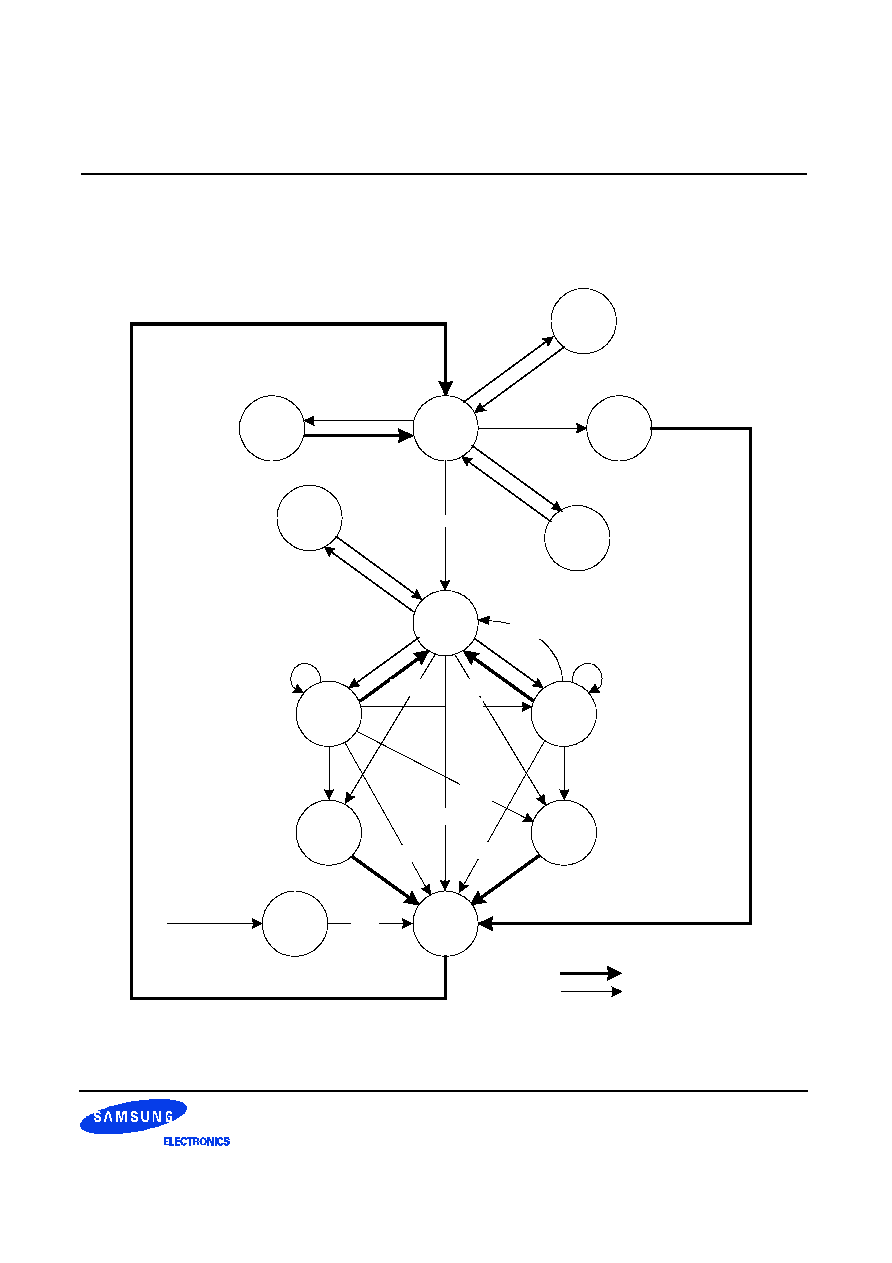
3.1 Simplified State Diagram
READ
SELF
REFRESH
AUTO
REFRESH
POWER
DOWN
ROW
ACTIVE
READA
WRITEA
WRITEA
PRE
CHARGE
POWER
ON
IDLE
MODE
POWER
DOWN
REGISTER
SET
REFS
REFSX
REFA
MRS
CKEL
CKEH
ACT
CKEL
CKEH
WRITE
WRITE
WRITEA
PRE
PRE
POWER
APPLIED
READA
PRE
PRE
READA
WRITEA
READA
READ
READ
Automatic Sequence
Command Sequence
BURST STOP
WRITEA : Write with autoprecharge
READA : Read with autoprecharge
Figure 3. State diagram

- 14 of 63 -
REV. 0.61 August 9. '99
128Mb DDR SDRAM
Target
3.2.1 Power-Up and Initialization Sequence
The following sequence is required for POWER UP and Initialization.
1. Apply power and attempt to maintain CKE at a low state(all other inputs may be undefined.)
- Apply VDD before or at the same time as VDDQ.
- Apply VDDQ before or at the same time as VTT & Vref.
2. Start clock and maintain stable condition for a minimum of 200us.
3. The minimum of 200us after stable power and clock(CK, CK), apply NOP & take CKE high.
4. Issue precharge commands for all banks of the device.
5. Issue EMRS to enable DLL.(To issue "DLL Enable" command, provide "Low" to A0, "High" to BA0 and "Low"
to all of the rest address pins, A1~A11 and BA1)
6. Issue a mode register set command for "DLL reset". The additional 200 cycles of clock input is required to
lock the DLL.
(To issue DLL reset command, provide "High" to A8 and "Low" to BA0)
7. Issue precharge commands for all banks of the device.
8. Issue 2 or more auto-refresh commands.
9. Issue a mode register set command with low to A8 to initialize device operation.
*1 Every "DLL enable" command resets DLL. Therefore sequence 6 can be skipped during power up.
Instead of it, the additional 200 cycles of clock input is required to lock the DLL after enabling DLL.
*2 Sequence of 6 & 7 is regardless of the order.
Power up & Initialization Sequence
Command
0
1
2
3
4
5
6
7
8
9
10
11
12
13
14
15
16
17
18
19
t
RP
2 Clock min.
precharge
ALL Banks
2nd Auto
Refresh
Mode
Register Set
Any
Command
t
RFC
1st Auto
Refresh
t
RFC
min.200 Cycle
EMRS
MRS
2 Clock min.
DLL Reset
*1
*2
*1
2 Clock min.
precharge
ALL Banks
t
RP
CK
CK
3.2 Basic Functionality
Figure 4. Power up and initialization sequence
- 15 of 63 -
REV. 0.61 August 9. '99
128Mb DDR SDRAM
Target
3.2.2 Mode Register Definition
3.2.2.1 Mode Register Set(MRS)
The mode register stores the data for controlling the various operating modes of DDR SDRAM. It programs
CAS latency, addressing mode, burst length, test mode, DLL reset and various vendor specific options to make
DDR SDRAM useful for variety of different applications. The default value of the mode register is not defined,
therefore the mode register must be written after EMRS setting for proper DDR SDRAM operation. The mode
register is written by asserting low on CS, RAS, CAS, WE and BA0(The DDR SDRAM should be in all bank pre-
charge with CKE already high prior to writing into the mode register). The states of address pins A0 ~ A11 in
the same cycle as CS, RAS, CAS, WE and BA0 going low are written in the mode register. Two clock cycles
are requested to complete the write operation in the mode register. The mode register contents can be
changed using the same command and clock cycle requirements during operation as long as all banks are in
the idle state. The mode register is divided into various fields depending on functionality. The burst length uses
A0 ~ A2, addressing mode uses A3, CAS latency(read latency from column address) uses A4 ~ A6. A7 is used
for test mode. A8 is used for DLL reset. A7 must be set to low for normal MRS operation. Refer to the table for
specific codes for various burst lengths, addressing modes and CAS latencies.
Address Bus
CAS Latency
A
6
A
5
A
4
Latency
0
0
0
Reserved
0
0
1
Reserved
0
1
0
2
0
1
1
Reserved
1
0
0
Reserved
1
0
1
Reserved
1
1
0
2.5
1
1
1
Reserved
Burst Length
A
2
A
1
A
0
Latency
Sequential
Interleave
0
0
0
Reserve
Reserve
0
0
1
2
2
0
1
0
4
4
0
1
1
8
8
1
0
0
Reserve
Reserve
1
0
1
Reserve
Reserve
1
1
0
Reserve
Reserve
1
1
1
Reserve
Reserve
A
7
mode
0
Normal
1
Test
A
3
Burst Type
0
Sequential
1
Interleave
* RFU(Reserved for future use)
should stay "0" during MRS
cycle.
A
8
DLL Reset
0
No
1
Yes
Mode Register
BA
1
BA
0
A
11
A
10
A
9
A
8
A
7
A
6
A
5
A
4
A
3
A
2
A
1
A
0
RFU
TM
CAS Latency
BT
Burst Length
RFU
DLL
0
BA
0
A
n
~ A
0
0
(Existing)MRS Cycle
1
Extended Funtions(EMRS)
Figure 5. Mode Register Set

- 16 of 63 -
REV. 0.61 August 9. '99
128Mb DDR SDRAM
Target
Mode Register Set
*1 : MRS can be issued only at all bank precharge state.
*2 : Minimum
t
RP
is required to issue MRS command.
Command
2
0
1
5
3
4
8
6
7
t
CK
2 Clock min.
Precharge
All Banks
Mode
Register Set
t
RP
*2
*1
Any
Command
CK
CK
Burst Address Ordering for Burst Length
Burst
Length
Starting
Address(A2, A1, A0)
Sequential Mode
Interleave Mode
2
xx0
0, 1
0, 1
xx1
1, 0
1, 0
4
x00
0, 1, 2, 3
0, 1, 2, 3
x01
1, 2, 3, 0
1, 0, 3, 2
x10
2, 3, 0, 1
2, 3, 0, 1
x11
3, 0, 1, 2
3, 2, 1, 0
8
000
0, 1, 2, 3, 4, 5, 6, 7
0, 1, 2, 3, 4, 5, 6, 7
001
1, 2, 3, 4, 5, 6, 7, 0
1, 0, 3, 2, 5, 4, 7, 6
010
2, 3, 4, 5, 6, 7, 0, 1
2, 3, 0, 1, 6, 7, 4, 5
011
3, 4, 5, 6, 7, 0, 1, 2
3, 2, 1, 0, 7, 6, 5, 4
100
4, 5, 6, 7, 0, 1, 2, 3
4, 5, 6, 7, 0, 1, 2, 3
101
5, 6, 7, 0, 1, 2, 3, 4
5, 4, 7, 6, 1, 0, 3, 2
110
6, 7, 0, 1, 2, 3, 4, 5
6, 7, 4, 5, 2, 3, 0, 1
111
7, 0, 1, 2, 3, 4, 5, 6
7, 6, 5, 4, 3, 2, 1, 0
DLL Enable/Disable
The DLL must be enabled for normal operation. DLL enable is required during power-up initialization, and
upon returing to normal operation after having disabled the DLL for the purpose of debug or evaluation (upon
exiting Self Refresh Mode, the DLL is enabled automatically). Any time the DLL is enabled, 200 clock cycles
must occur before a READ command can be issued.
Output Drive Strength
The normal drive strength for all outputs is specified to be SSTL_2, Class II. Some vendors might also support
a weak driver strength option, intended for lighter load and/or point-to-point environments. I-V curves for the
normal drive strength and weak drive strength will be included in a future revision of this document.
Table 4. Burst address ordering for burst length
Figure 6. Mode Register Set sequence
- 17 of 63 -
REV. 0.61 August 9. '99
128Mb DDR SDRAM
Target
3.2.2.2 Extended Mode Register Set(EMRS)
The extended mode register stores the data for enabling or disabling DLL, QFC and selecting output driver
size. The default value of the extended mode register is not defined, therefore the extened mode register must
be written after power up for enabling or disabling DLL. The extended mode register is written by asserting low
on CS, RAS, CAS, WE and high on BA0(The DDR SDRAM should be in all bank precharge with CKE already
high prior to writing into the extended mode register). The state of address pins A0 ~ A11 and BA1 in the
same cycle as CS, RAS, CAS and WE going low are written in the extended mode register. Two clock cycles
are required to complete the write operation in the extended mode register. The mode register contents can
be changed using the same command and clock cycle requirements during operation as long as all banks are
in the idle state. A0 is used for DLL enable or disable. "High" on BA0 is used for EMRS. All the other address
pins except A0 and BA0 must be set to low for proper EMRS operation. Refer to the table for specific codes.
Address Bus
RFU
RFU : Must be set "0"
Extended Mode Register
DLL
BA
1
BA
0
A
11
A
10
A
9
A
8
A
7
A
6
A
5
A
4
A
3
A
2
A
1
A
0
1
A
0
DLL Enable
0
Enable
1
Disable
BA
0
A
n
~ A
0
0
(Existing)MRS Cycle
1
Extended Funtions(EMRS)
QFC control
0
Disable(Default)
1
Enable
Output Driver Impedence Control
0
Normal
1
Weak
QFC D.I.C
Figure 7. Extend Mode Register set
- 18 of 63 -
REV. 0.61 August 9. '99
128Mb DDR SDRAM
Target
3.2.3 Precharge
3.2.4 No Operation(NOP) & Device Deselect
The precharge command is used to precharge or close a bank that has been activated. The precharge com-
mand is issued when CS, RAS and WE are low and CAS is high at the rising edge of the clock. The precharge
command can be used to precharge each bank respectively or all banks simultaneously. The bank select
addresses(BA0, BA1) are used to define which bank is precharged when the command is initiated. For write
cycle, tWR(min.) must be satisfied until the precharge command can be issued. After tRP from the precharge,
an active command to the same bank can be initiated.
A10/AP
BA1
BA0
Precharge
0
0
0
Bank A Only
0
0
1
Bank B Only
0
1
0
Bank C Only
0
1
1
Bank D Only
1
X
X
All Banks
The device should be deselected by deactivating the CS signal. In this mode DDR SDRAM should ignore
all the control inputs. The DDR SDRAMs are put in NOP mode when CS is active and by deactivating RAS,
CAS and WE. For both Deselect and NOP the device should finish the current operation when this com-
mand is issued.
Bank Selection for Precharge by Bank address bits
Table 5. Bank selection for precharge by Bank address bits
- 19 of 63 -
REV. 0.61 August 9. '99
128Mb DDR SDRAM
Target
3.2.5 Row Active
The Bank Activation command is issued by holding CAS and WE high with CS and RAS low at the rising
edge of the clock(CK). The DDR SDRAM has four independent banks, so two Bank Select addresses(BA0,
BA1) are required. The Bank Activation command must be applied before any Read or Write operation is exe-
cuted. The delay from the Bank Activation command to the first read or write command must meet or exceed
the minimum of RAS to CAS delay time(tRCD min). Once a bank has been activated, it must be precharged
before another Bank Activation command can be applied to the same bank. The minimum time interval
between interleaved Bank Activation commands(Bank A to Bank B and vice versa) is the Bank to Bank delay
time(tRRD min).
Address
Command
RAS-CAS delay(
t
RCD
)
Bank Activation Command Cycle
(CAS Latency = 2)
Bank A
Row Addr.
Bank A
Col. Addr.
Bank A
Activate
Write A
with Auto
NOP
Precharge
RAS-RAS delay time(
t
RRD
)
Bank B
Row Addr.
Bank A
Row. Addr.
Bank B
Activate
Bank A
Activate
NOP
ROW Cycle Time(
t
RC
)
Tn
Tn+1
Tn+2
2
0
1
: Don
t care
CK
CK
3.2.6 Read Bank
3.2.7 Write Bank
This command is used after the row activate command to initiate the burst read of data. The read command
is initiated by activating RAS, CS, CAS, and deasserting WE at the same clock sampling(rising) edge as
described in the command truth table. The length of the burst and the CAS latency time will be determined by
the values programmed during the MRS command.
This command is used after the row activate command to initiate the burst write of data. The write com-
mand is initiated by activating RAS, CS, CAS, and WE at the same clock sampling(rising) edge as described in
the command truth table. The length of the burst will be determined by the values programmed during the
MRS command.
Figure 8. Bank activation command cycle timing

- 20 of 63 -
REV. 0.61 August 9. '99
128Mb DDR SDRAM
Target
3.3.1 Burst Read Operation
Burst Read operation in DDR SDRAM is in the same manner as the current SDRAM such that the Burst read
command is issued by asserting CS and CAS low while holding RAS and WE high at the rising edge of the
clock(CK) after tRCD from the bank activation. The address inputs (A0~A9) determine the starting address for
the Burst. The Mode Register sets type of burst(Sequential or interleave) and burst length(2, 4, 8). The first
output data is available after the CAS Latency from the READ command, and the consecutive data are pre-
sented on the falling and rising edge of Data Strobe(DQS) adopted by DDR SDRAM until the burst length is
completed.
Command
< Burst Length=4, CAS Latency= 2, 2.5 >
READ A
NOP
NOP
NOP
NOP
NOP
NOP
NOP
NOP
DQS
DQ
s
CAS Latency=2
Dout 0 Dout 1 Dout 2 Dout 3
DQS
DQ
s
CAS Latency=2.5
Dout 0 Dout 1 Dout 2 Dout 3
2
0
1
5
3
4
8
6
7
t
RPRE
t
RPST
CK
CK
3.3 Essential Functionality for DDR SDRAM
The essential functionality that is required for the DDR SDRAM device is described in this chapter
Figure 9. Burst read operation timing
- 21 of 63 -
REV. 0.61 August 9. '99
128Mb DDR SDRAM
Target
3.3.2 Burst Write Operation
The Burst Write command is issued by having CS, CAS, and WE low while holding RAS high at the rising
edge of the clock(CK). The address inputs determine the starting column address. There is no write latency
relative to DQS required for burst write cycle. The first data of a burst write cycle must be applied on the DQ
pins tDS(Data-in setup time) prior to data strobe edge enabled after tDQSS from the rising edge of the
clock(CK) that the write command is issued. The remaining data inputs must be supplied on each subsequent
falling and rising edge of Data Strobe until the burst length is completed. When the burst has been finished, any
additional data supplied to the DQ pins will be ignored.
Figure 10. Burst write operation timing
1. The soecific requirement is that DQS be valid(High or Low) on or before this CK edge. The case shown
(DQS going from High_Z to logic Low) applies when no writes were previously in progress on the bus.
If a previous write was in progress, DQS could be High at this time, depending on tDQSS.
(Refer to AC parameter table in page 42)
*1
Command
< Burst Length=4 >
NOP
WRITEA
NOP
NOP
NOP
WRITEB
NOP
NOP
NOP
DQS
DQ
s
Din 3
Din 0 Din 1
Din 2
t
DQSSmax
2
0
1
5
3
4
8
6
7
t
WPRES*1
CK
CK
Din 3
Din 0 Din 1
Din 2
- 22 of 63 -
REV. 0.61 August 9. '99
128Mb DDR SDRAM
Target
3.3.3 Read Interrupted by a Read
A Burst Read can be interrupted before completion of the burst by new Read command of any bank. When
the previous burst is interrupted, the remaining addresses are overridden by the new address with the full burst
length. The data from the first Read command continues to appear on the outputs until the CAS latency from
the interrupting Read command is satisfied. At this point the data from the interrupting Read command
appears. Read to Read interval is minimum 1 Clock.
Command
< Burst Length=4, CAS Latency=2 >
READ A
READ B
NOP
NOP
NOP
NOP
NOP
NOP
NOP
DQS
DQ
s
CAS Latency=2
D
out
A
0
D
out
A
1
D
out
B
0
D
out
B
1
D
out
B
2
D
out
B
3
2
0
1
5
3
4
8
6
7
CK
CK
3.3.4 Read Interrupted by a Write & Burst Stop
To interrupt a burst read with a write command, Burst Stop command must be asserted to avoid data conten-
tion on the I/O bus by placing the DQ
'
s(Output drivers) in a high impedance state. To insure the DQ
'
s are tri-
stated one cycle before the beginning the write operation, Burst stop command must be applied at least 2
clock cycles for CL=2 and at least 3 clock cycles for CL=2.5 before the Write command.
Command
< Burst Length=4, CAS Latency=2 >
READ
Burst Stop
NOP
WRITE
NOP
NOP
NOP
NOP
NOP
DQS
DQ
s
CAS Latency=2
Dout 0 Dout 1
Din 0
Din 1
Din 2
Din 3
2
0
1
5
3
4
8
6
7
CK
CK
The following functionality establishes how a Write command may interrupt a Read burst.
1. For Write commands interrupting a Read burst, a Burst Terminate command is required to stop the read
burst and tristate the DQ bus prior to valid input write data. Once the Burst Terminate command has been
issued, the minimum delay to a Write command = RU(CL) [CL is the CAS Latency and RU means round up
to the nearest integer].
2. It is illegal for a Write command to interrupt a Read with autoprecharge command.
Figure 11. Read interrupted by a read timing
Figure 12. Read interrupted by a write and burst stop timing.
- 23 of 63 -
REV. 0.61 August 9. '99
128Mb DDR SDRAM
Target
3.3.5 Read Interrupted by a Precharge
A Burst Read operation can be interrupted by precharge of the same bank. The minimum 1 clock is required
for the read to precharge intervals. A precharge command to output disable latency is equivalent to the CAS
latency.
Command
< Burst Length=8, CAS Latency=2 >
READ
NOP
Precharge
NOP
NOP
NOP
NOP
NOP
NOP
DQS
DQ
s
CAS Latency=2
Dout 0
Dout 1
Dout 2
Dout 3
Interrupted by precharge
2
0
1
5
3
4
8
6
7
Dout 4
Dout 5 Dout 6
Dout 7
1t
CK
CK
CK
When a burst Read command is issued to a DDR SDRAM, a Precharge command may be issued to the same
bank before the Read burst is complete. The following functionality determines when a Precharge command
may be given during a Read burst and when a new Bank Activate command may be issued to the same bank.
1. For the earliest possible Precharge command without interrupting a Read burst, the Precharge command
may be given on the rising clock edge which is CL clock cycles before the end of the Read burst where CL
is the CAS Latency. A new Bank Activate command may be issued to the same bank after tRP (RAS
Precharge time).
2. When a Precharge command interrupts a Read burst operation, the Precharge command may be given on
the rising clock edge which is CL clock cycles before the last data from the interrupted Read burst where
CL is the CAS Latency. Once the last data word has been output, the output buffers are tristated. A new
Bank Activate command may be issued to the same bank after tRP.
3. For a Read with autoprecharge command, a new Bank Activate command may be issued to the same
bank after tRP where tRP begins on the rising clock edge which is CL clock cycles before the end of the
Read burst where CL is the CAS Latency. During Read with autoprecharge, the initiation of the internal
precharge occurs at the same time as the earliest possible external Precharge command would initiate a
precharge operation without interrupting the Read burst as described in 1 above.
4. For all cases above, tRP is an analog delay that needs to be converted into clock cycles. The number of
clock cycles between a Precharge command and a new Bank Activate command to the same bank equals
tRP/tCK (where tCK is the clock cycle time) with the result rounded up to the nearest integer number of
clock cycles. (Note that rounding to X.5 is not possible since the Precharge and Bank Activate commands
can only be given on a rising clock edge).
In all cases, a Precharge operation cannot be initiated unless tRAS(min) [minimum Bank Activate to Precharge
time] has been satisfied. This includes Read with autoprecharge commands where tRAS(min) must still be
satisfied such that a Read with autoprecharge command has the same timing as a Read command followed by
the earliest possible Precharge command which does not interrupt the burst.
Figure 13. Read interrupted by a precharge timing
- 24 of 63 -
REV. 0.61 August 9. '99
128Mb DDR SDRAM
Target
3.3.6 Write Interrupted by a Write
A Burst Write can be interrupted before completion of the burst by a new Write command, with the only restric-
tion that the interval that separates the commands must be at least one clock cycle. When the previous burst
is interrupted, the remaining addresses are overridden by the new address and data will be written into the
device until the programmed burst length is satisfied.
Command
< Burst Length=4 >
NOP
WRITE A
WRITE b
NOP
NOP
NOP
NOP
NOP
NOP
DQS
DQ
s
Din A
0
Din A
1
Din B
0
Din B
1
Din B
2
Din B
3
1t
CK
2
0
1
5
3
4
8
6
7
CK
CK
Figure 14. Write interrupted by a write timing
- 25 of 63 -
REV. 0.61 August 9. '99
128Mb DDR SDRAM
Target
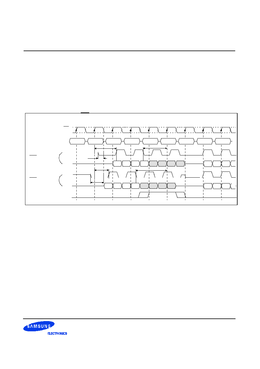
3.3.7 Write Interrupted by a Read & DM
A burst write can be interrupted by a read command of any bank. The DQ
'
s must be in the high impedance
state at least one clock cycle before the interrupting read data appear on the outputs to avoid data contention.
When the read command is registered, any residual data from the burst write cycle must be masked by DM.
The delay from the last data to read command (tCDLR) is required to avoid the data contention DRAM inside.
Data that are presented on the DQ pins before the read command is initiated will actually be written to the
memory. Read command interrupting write can not be issued at the next clock edge of that of write command.
Command
< Burst Length=8, CAS Latency=2 >
NOP
WRITE
NOP
NOP
READ
NOP
NOP
NOP
NOP
DQS
DQ
s
Din 0
Din 1
Din 2
Din 3
Din 4
Din 5
Dout 0 Dout 1 Dout 2
Din 6
Din 7
t
CDLR
CAS Latency=2
t
DQSSmax
DQS
DQ
s
t
CDLR
CAS Latency=2
t
DQSSmin
Din 7
Din 0
Din 1
Din 2
Din 3
Din 4
Din 5
Din 6
DM
Do
Dout 0 Dout 1 Dout 2 Do
2
0
1
5
3
4
8
6
7
t
WPRES
t
WPRES
CK
CK
The following function established how a Read command may interrupt a Write burst and which input data is
not written into the memory.
1. For Read commands interrupting a Write burst, the minimum Write to Read command delay is 2 clock
cycles. The case where the Write to Read delay is 1 clock cycle is disallowed
2. For Read commands interrupting a Write burst, the DM pin must be used to mask the input data words
whcich immediately precede the interrupting Read operation and the input data word which immediately
follows the interrupting Read operation
3. For all cases of a Read interrupting a Write, the DQ and DQS buses must be released by the driving chip
(i.e., the memory controller) in time to allow the buses to turn around before the DDR SDRAM drives them
during a read operation.
4. If input Write data is masked by the Read command, the DQS input is ignored by the DDR SDRAM
Figure 15. Write interrupted by a read and DM timing

- 26 of 63 -
REV. 0.61 August 9. '99
128Mb DDR SDRAM
Target
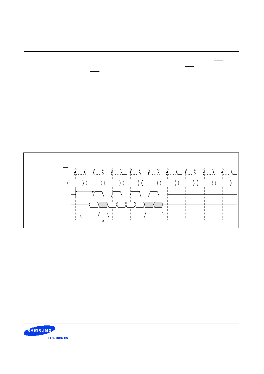
3.3.8 Write Interrupted by a Precharge & DM
A burst write operation can be interrupted before completion of the burst by a precharge of the same bank.
Random column access is allowed. A write recovery time(tWR) is required from the last data to precharge
command. When precharge command is asserted, any residual data from the burst write cycle must be
masked by DM.
Command
< Burst Length=8 >
NOP
WRITE A
NOP
NOP
Precharge
NOP
NOP
NOP
WRITEB
DQS
DQ
s
Dina
0
Dina
1
Dina
2
Dina
3
Dina
4
Dina
5
Dinb
0
Dina
6
Dina
7
t
WR
DQS
DQ
s
t
DQSSmin
Dina
7
Dina
0
Dina
1
Dina
2
Dina
3
Dina
4
Dina
5
Dina
6
DM
Dinb
0
Dinb
1
t
DQSSmax
2
0
1
5
3
4
8
6
7
CK
CK
Precharge timing for Write operations in DRAMs requires enough time to allow "write recovery" which is the
time required by a DRAM core to properly store a full "0" or "1" level before a Precharge operation. For DDR
SDRAM, a timing parameter, tWR, is used to indicate the required amount of time between the last valid write
operation and a Precharge command to the same bank.
The precharge timing for writes is a complex definition since the write data is sampled by the data strobe and
the address is sampled by the input clock. Inside the SDRAM, the data path is eventually synchronized with
the address path by switching clock domains from the data strobe clock domain to the input clock domain.
This makes the definition of when a precharge operation can be initiated after a write very complex since the
write recovery parameter must reference only the clock domain that is used to time the internal write operation,
i.e., the input clock domain.
tWR starts on the rising clock edge after the last possible DQS edge that strobed in the last valid data and
ends on the rising clock edge that strobes in the precharge command.
1. For the earliest possible Precharge command following a Write burst without interrupting the burst, the
minimum time for write recovery is defined by tWR.
2. When a precharge command interrupts a Write burst operation, the data mask pin, DM, is used to mask
input data during the time between the last valid write data and the rising clock edge on which the
Precharge command is given. During this time, the DQS input is still required to strobe in the state of DM.
The minimum time for write recovery is defined by tWR.
Figure 16. Write interrupted by a precharge and DM timing

- 27 of 63 -
REV. 0.61 August 9. '99
128Mb DDR SDRAM
Target
3. For a Write with autoprecharge command, a new Bank Activate command may be issued to the same
bank after tWR+tRP where tWR+tRP starts on the falling DQS edge that strobed in the last valid data and
ends on the rising clock edge that strobes in the Bank Activate command. During write with
autoprecharge, the initiation of the internal precharge occurs at the same time as the earliest possible
external Precharge command without interrupting the Write burst as described in 1 above.
4. In all cases, a Precharge operation cannot be initiated unless tRAS(min) [minimum Bank Activate to
Precharge time] has been satisfied. This includes Write with autoprecharge commands where tRAS(min)
must still be satisfied such that a Write with autoprecharge command has the same timing as a Write
command followed by the earliest possible Precharge command which does not interrupt the burst.
3.3.9 Burst Stop
The burst stop command is initiated by having RAS and CAS high with CS and WE low at the rising edge of
the clock(CK). The burst stop command has the fewest restrictions making it the easiest method to use when
terminating a burst read operation before it has been completed. When the burst stop command is issued dur-
ing a burst read cycle, the pair of data and DQS(Data Strobe) go to a high impedance state after a delay which
is equal to the CAS latency set in the mode register. The burst stop command, however, is not supported dur-
ing a write burst operation.
Command
< Burst Length=4, CAS Latency= 2, 2.5 >
READ A
Burst Stop
NOP
NOP
NOP
NOP
NOP
NOP
NOP
DQS
DQ
s
CAS Latency=2
Dout 0 Dout 1
DQS
DQ
s
CAS Latency=2.5
The burst ends after a delay equal to the CAS latency.
Dout 0 Dout 1
2
0
1
5
3
4
8
6
7
CK
CK
The Burst Stop command is a mandatory feature for DDR SDRAMs. The following functionality is required:
1. The BST command may only be issued on the rising edge of the input clock, CK.
2. BST is only a valid command during Read bursts.
3. BST during a Write burst is undefined and shall not be used.
4. BST applies to all burst lengths.
5. BST is an undefined command during Read with autoprecharge and shall not be used.
Figure 17. Burst stop timing
- 28 of 63 -
REV. 0.61 August 9. '99
128Mb DDR SDRAM
Target
3.3.10 DM masking
The DDR SDRAM has a data mask function that can be used in conjunction with data write cycle, not read
cycle. When the data mask is activated (DM high) during write operation, DDR SDRAM does not accept the
corresponding data.(DM to data-mask latency is zero).
DM must be issued at the rising or falling edge of data strobe.
Command
< Burst Length=8 >
WRITE
NOP
NOP
NOP
NOP
NOP
NOP
NOP
NOP
DQS
DQ
s
Din 0
Din 1 Din 2
Din 3
t
DQSS
DM
Din 4
Din 5 Din 6
Din7
masked by DM=H
2
0
1
5
3
4
8
6
7
CK
CK
6. When terminating a burst Read command, the BST command must be issued L
BST
("BST Latency") clock
cycles before the clock edge at which the output buffers are tristated, where L
BST
equals the CAS latency
for read operations. This is shown in previous page Figure with examples for CAS latency (CL) of 1.5, 2,
2.5, 3 and 3.5 (only selected CAS latencies are required by the DDR SDRAM standards, the others are
optional).
7. When the burst terminates, the DQ and DQS pins are tristated.
The BST command is not byte controllable and applies to all bits in the DQ data word and the(all) DQS pin(s).
Figure 18. DM masking timing
- 29 of 63 -
REV. 0.61 August 9. '99
128Mb DDR SDRAM
Target
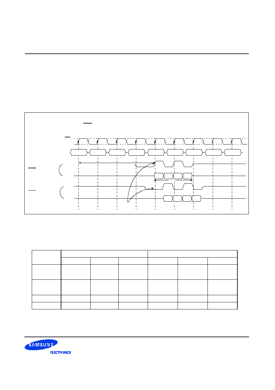
Command
< Burst Length=4, CAS Latency= 2, 2.5>
BANK A
NOP
READ A
NOP
NOP
NOP
NOP
NOP
NOP
DQS
DQ
s
CAS Latency=2
Dout 0 Dout 1 Dout 2 Dout 3
ACTIVE
Auto Precharge
* Bank can be reactivated at the
t
RP
completion of
precharge
Begin Auto-Precharge
DQS
DQ
s
CAS Latency=2.5
Dout 0 Dout 1 Dout 2 Dout 3
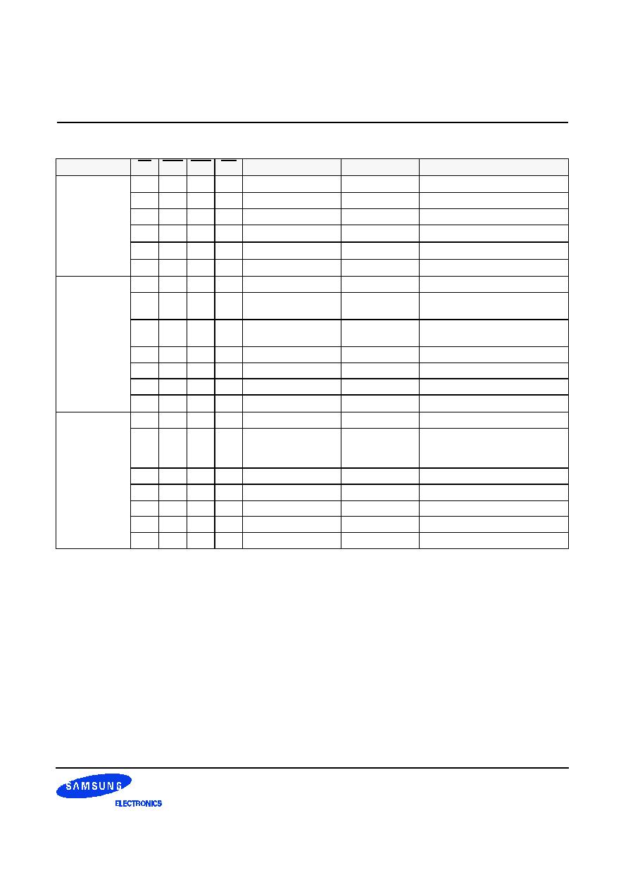
When the Read with Auto precharge command is issued, new command can be asserted at 3,4 and 5
respectively as follows,
Asserted
command
For same Bank
For Different Bank
3
4
5
3
4
5
READ
READ +
No AP
*1
READ+
No AP
Illegal
Legal
Legal
Legal
READ+AP
READ +
AP
READ +
AP
Illegal
Legal
Legal
Legal
Active
Illegal
Illegal
Illegal
Legal
Legal
Legal
Precharge
Legal
Legal
Illegal
Legal
Legal
Legal
*1
: AP = Auto Precharge
2
0
1
5
3
4
8
6
7
t
RAS(min.)
CK
CK
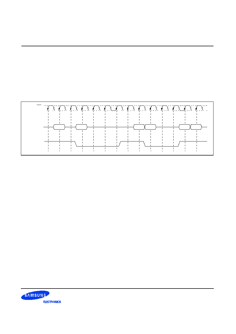
3.3.11 Read With Auto Precharge
If a read with auto-precharge command is initiated, the DDR SDRAM automatically enters the precharge
operation BL/2 clock later from a read with auto-precharge command when tRAS(min) is satisfied. If not, the
start point of precharge operation will be delayed until tRAS(min) is satisfied. Once the precharge operation
has started the bank cannot be reactivated and the new command can not be asserted until the precharge
time(tRP) has been satisfied.
Figure 19. Read with auto precharge timing
Table 6. Operating description when new command asserted
while read with auto precharge is issued
- 30 of 63 -
REV. 0.61 August 9. '99
128Mb DDR SDRAM
Target
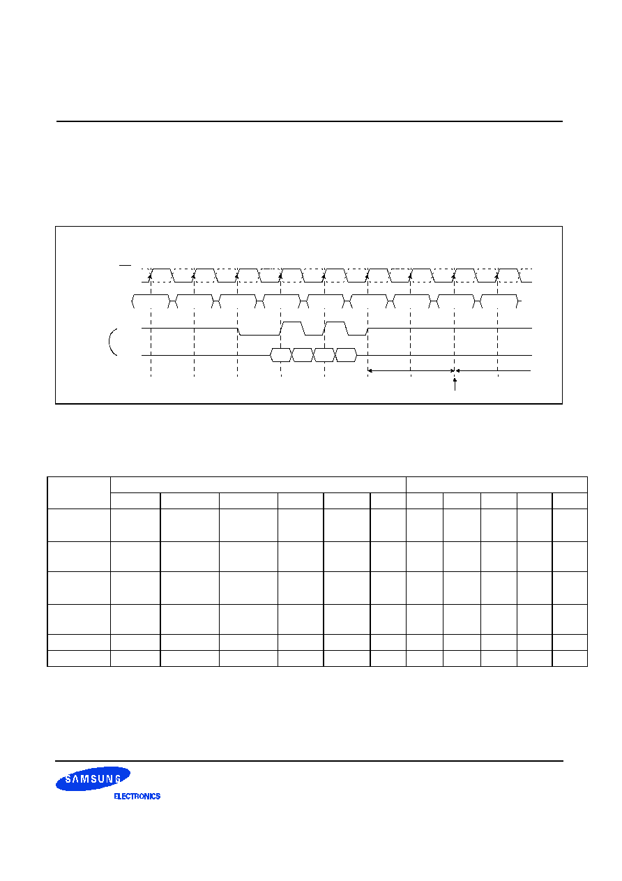
3.3.12 Write with Auto Precharge
If A10 is high when write command is issued , the write with auto-precharge function is performed. Any new
command to the same bank should not be issued until the internal precharge is completed. The internal pre-
charge begins after keeping tWR(min).
Command
< Burst Length=4 >
BANK A
NOP
WRITE A
NOP
NOP
NOP
NOP
NOP
NOP
DQS
DQ
s
Din 0 Din 1 Din 2
Din 3
ACTIVE
Auto Precharge
* Bank can be reactivated at
completion of
t
RP
t
WR
t
RP
Internal precharge start
2
0
1
5
3
4
8
6
7
CK
CK
Figure 20. Write with auto precharge timing
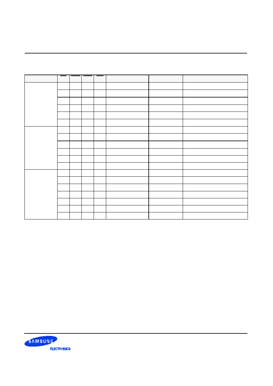
Asserted
command
For same Bank
For Different Bank
3
4
5
6
7
8
3
4
5
6
7
WRITE
WRITE+
No AP
*1
WRITE+
No AP
WRITE+
No AP
Illegal
Illegal
Illegal
Legal
Legal
Legal
Legal
Legal
WRITE+
AP
WRITE+
AP
WRITE+
AP
WRITE+
AP
Illegal
Illegal
Illegal
Legal
Legal
Legal
Legal
Legal
READ
Illegal
READ+NO
AP+DM
*2
READ+NO
AP+DM
READ+
NO AP
READ+
NO AP
Illegal
Illegal
Illegal
Legal
Legal
Legal
READ+AP
Illegal
READ +
AP+DM
READ +
AP+DM
READ +
AP
READ +
AP
Illegal
Illegal
Illegal
Legal
Legal
Legal
Active
Illegal
Illegal
Illegal
Illegal
Illegal
Illegal
Legal
Legal
Legal
Legal
Legal
Precharge
Illegal
Illegal
Illegal
Illegal
Illegal
Illegal
Legal
Legal
Legal
Legal
Legal
*1
: AP = Auto Precharge
*2
: DM : Refer to " 3.3.7 Write Interrupted by a Read & DM " in page 25.
Burst length = 4
Table 7. Operating description when new command asserted
while write with auto precharge is issued

- 31 of 63 -
REV. 0.61 August 9. '99
128Mb DDR SDRAM
Target
3.3.13 Auto Refresh & Self Refresh
Auto Refresh
Command
CKE
PRE
t
RP
t
RFC
Auto
= High
Refresh
CMD
An auto refresh command is issued by having CS, RAS and CAS held low with CKE and WE high at the ris-
ing edge of the clock(CK). All banks must be precharged and idle for tRP(min) before the auto refresh com-
mand is applied. No control of the external address pins is required once this cycle has started because of the
internal address counter. When the refresh cycle has completed, all banks will be in the idle state. A delay
between the auto refresh command and the next activate command or subsequent auto refresh command
must be greater than or equal to the tRFC(min).
CK
CK
Self Refresh
A self refresh command is defined by having CS, RAS, CAS and CKE held low with WE high at the rising
edge of the clock(CK). Once the self refresh command is initiated, CKE must be held low to keep the device in
self refresh mode. During the self refresh operation, all inputs except CKE are ignored. The clock is internally
disabled during self refresh operation to reduce power consumption. The self refresh is exited by supplying
stable clock input before returning CKE high, asserting deselect or NOP command and then asserting CKE
high for longer than tXSR for locking of DLL.
Command
CKE
t
XSA
Self
Refresh
CK
CK
Read
t
XSR
Figure 21. Auto refresh timing
Figure 22. Self refresh timing
Active
- 32 of 63 -
REV. 0.61 August 9. '99
128Mb DDR SDRAM
Target
3.3.14 Power down
CKE
Precharge
Active
Active
Read
power
down
Exit
Active
power
down
Entry
power
Entry
down
Precharge
Command
CK
CK
The power down mode is entered when CKE is low and exited when CKE is high. Once the power down
mode is initiated, all of the receiver circuits except clock, CKE and DLL circuit tree are gated off to reduce
power consumption. The all banks should be in idle state prior to entering the precharge power down mode
and CKE should be set high at least 1tck+tIS prior to row active command . During power down mode, refresh
operations cannot be performed, therefore the device cannot remain in power down mode longer than the
refresh period(tREF) of the device.
Figure 23. Power down entry and exit timing

- 33 of 63 -
REV. 0.61 August 9. '99
128Mb DDR SDRAM
Target
4. Command Truth Table
(V=Valid, X=Don
t Care, H=Logic High, L=Logic Low)
COMMAND
CKEn-1
CKEn
CS
RAS
CAS
WE
DM
BA
0,1
A
10
/AP
A
11,
A
9
~ A
0
Note
Register
Extended MRS
H
X
L
L
L
L
X
OP CODE
1, 2
Register
Mode Register Set
H
X
L
L
L
L
X
OP CODE
1, 2
Refresh
Auto Refresh
H
H
L
L
L
H
X
X
3
Self
Refresh
Entry
L
3
Exit
L
H
L
H
H
H
X
X
3
H
X
X
X
3
Bank Active & Row Addr.
H
X
L
L
H
H
X
V
Row Address
Read &
Column Address
Auto Precharge Disable
H
X
L
H
L
H
X
V
L
Column
Address
(A
0
~A
9
)
4
Auto Precharge Enable
H
4
Write &
Column Address
Auto Precharge Disable
H
X
L
H
L
L
X
V
L
Column
Address
(A
0
~A
9
)
4
Auto Precharge Enable
H
4, 6
Burst Stop
H
X
L
H
H
L
X
X
7
Precharge
Bank Selection
H
X
L
L
H
L
X
V
L
X
All Banks
X
H
5
Active Power Down
Entry
H
L
H
X
X
X
X
X
L
V
V
V
Exit
L
H
X
X
X
X
X
Precharge Power Down Mode
Entry
H
L
H
X
X
X
X
X
L
H
H
H
Exit
L
H
H
X
X
X
X
L
V
V
V
DM
H
X
V
X
8
No operation (NOP) : Not defined
H
X
H
X
X
X
X
X
9
L
H
H
H
9
1. OP Code : Operand Code. A
0
~ A
11
& BA
0
~ BA
1
: Program keys. (@EMRS/MRS)
2.EMRS/ MRS can be issued only at all banks precharge state.
A new command can be issued 2 clock cycles after EMRS or MRS.
3. Auto refresh functions are same as the CBR refresh of DRAM.
The automatical precharge without row precharge command is meant by "Auto".
Auto/self refresh can be issued only at all banks precharge state.
4. BA
0
~ BA
1
: Bank select addresses.
If both BA
0
and BA
1
are "Low" at read, write, row active and precharge, bank A is selected.
If both BA
0
is "High" and BA
1
is "Low" at read, write, row active and precharge, bank B is selected.
If both BA
0
is "Low" and BA
1
is "High" at read, write, row active and precharge, bank C is selected.
If both BA
0
and BA
1
are "High" at read, write, row active and precharge, bank D is selected.
5. If A
10
/AP is "High" at row precharge, BA
0
and BA
1
are ignored and all banks are selected.
6. During burst write with auto precharge, new read/write command can not be issued.
Another bank read/write command can be issued after the end of burst.
New row active of the associated bank can be issued at t
RP
after the end of burst.
7. Burst stop command is valid at every burst length.
8. DM sampled at the rising and falling edges of the DQS and Data-in are masked at the both edges (Write DM latency is 0).
9. This combination is not defined for any function, which means "No Operation(NOP)" in DDR SDRAM.
Table 8. Command truth table
- 34 of 63 -
REV. 0.61 August 9. '99
128Mb DDR SDRAM
Target
5. Functional Truth Table
Current State
CS
RAS CAS
WE
Address
Command
Action
PRECHARGE
STANDBY
L
H
H
L
X
Burst Stop
ILLEGAL*2
L
H
L
X
BA, CA, A
10
READ/WRITE
ILLEGAL*2
L
L
H
H
BA, RA
Active
Bank Active, Latch RA
L
L
H
L
BA, A
10
PRE/PREA
ILLEGAL*4
L
L
L
H
X
Refresh
AUTO-Refresh*5
L
L
L
L
Op-Code, Mode-Add
MRS
Mode Register Set*5
ACTIVE
STANDBY
L
H
H
L
X
Burst Stop
NOP
L
H
L
H
BA, CA, A
10
READ/READA
Begin Read, Latch CA,
Determine Auto-Precharge
L
H
L
L
BA, CA, A
10
WRITE/WRITEA
Begin Write, Latch CA,
Determine Auto-Precharge
L
L
H
H
BA, RA
Active
Bank Active/ILLEGAL*2
L
L
H
L
BA, A
10
PRE/PREA
Precharge/Precharge All
L
L
L
H
X
Refresh
ILLEGAL
L
L
L
L
Op-Code, Mode-Add
MRS
ILLEGAL
READ
L
H
H
L
X
Burst Stop
Terminate Burst
L
H
L
H
BA, CA, A
10
READ/READA
Terminate Burst, Latch CA,
Begin New Read, Determine
Auto-Precharge*3
L
H
L
L
BA, CA, A
10
WRITE/WRITEA ILLEGAL
L
L
H
H
BA, RA
Active
Bank Active/ILLEGAL*2
L
L
H
L
BA, A
10
PRE/PREA
Terminate Burst, Precharge
L
L
L
H
X
Refresh
ILLEGAL
L
L
L
L
Op-Code, Mode-Add
MRS
ILLEGAL
Table 9-1. Functional truth table

- 35 of 63 -
REV. 0.61 August 9. '99
128Mb DDR SDRAM
Target
Current State
CS
RAS CAS
WE
Address
Command
Action
WRITE
L
H
H
L
X
Burst Stop
ILLEGAL
L
H
L
H
BA, CA, A
10
READ/READA
Terminate Burst With DM=High,
Latch CA, Begin Read, Deter-
mine Auto-Precharge*3
L
H
L
L
BA, CA, A
10
WRITE/WRITEA
Terminate Burst, Latch CA,
Begin new Write, Determine
Auto-Precharge*3
L
L
H
H
BA, RA
Active
Bank Active/ILLEGAL*2
L
L
H
L
BA, A
10
PRE/PREA
Terminate Burst With DM=High,
Precharge
L
L
L
H
X
Refresh
ILLEGAL
L
L
L
L
Op-Code, Mode-Add
MRS
ILLEGAL
READ with
AUTO
PRECHARGE
*6
(READA)
L
H
H
L
X
Burst Stop
ILLEGAL
L
H
L
H
BA, CA, A
10
READ/READA
*6
L
H
L
L
BA, CA, A
10
WRITE/WRITEA ILLEGAL
L
L
H
H
BA, RA
Active
*6
L
L
H
L
BA, A
10
PRE/PREA
*6
L
L
L
H
X
Refresh
ILLEGAL
L
L
L
L
Op-Code, Mode-Add
MRS
ILLEGAL
WRITE with
AUTO
RECHARGE
*7
(WRITEA)
L
H
H
L
X
Burst Stop
ILLEGAL
L
H
L
H
BA, CA, A
10
READ/READA
*7
L
H
L
L
BA, CA, A
10
WRITE/WRITEA *7
L
L
H
H
BA, RA
Active
*7
L
L
H
L
BA, A
10
PRE/PREA
*7
L
L
L
H
X
Refresh
ILLEGAL
L
L
L
L
Op-Code, Mode-Add
MRS
ILLEGAL
Table 9-2. Functional truth table
- 36 of 63 -
REV. 0.61 August 9. '99
128Mb DDR SDRAM
Target
Current State
CS
RAS CAS
WE
Address
Command
Action
PRECHARG-
ING
(DURING tRP)
L
H
H
L
X
Burst Stop
ILLEGAL*2
L
H
L
X
BA, CA, A
10
READ/WRITE
ILLEGAL*2
L
L
H
H
BA, RA
Active
ILLEGAL*2
L
L
H
L
BA, A
10
PRE/PREA
NOP*4(Idle after
t
RP
)
L
L
L
H
X
Refresh
ILLEGAL
L
L
L
L
Op-Code, Mode-Add
MRS
ILLEGAL
ROW
ACTIVATING
(FROM ROW
ACTIVE TO
tRCD)
L
H
H
L
X
Burst Stop
ILLEGAL*2
L
H
L
X
BA, CA, A
10
READ/WRITE
ILLEGAL*2
L
L
H
H
BA, RA
Active
ILLEGAL*2
L
L
H
L
BA, A
10
PRE/PREA
ILLEGAL*2
L
L
L
H
X
Refresh
ILLEGAL
L
L
L
L
Op-Code, Mode-Add
MRS
ILLEGAL
WRITE
RECOVERING
(DURING tWR
OR tCDLR)
L
H
H
L
X
Burst Stop
ILLEGAL*2
L
H
L
H
BA, CA, A
10
READ
ILLEGAL*2
L
H
L
L
BA, CA, A
10
WRITE
WRITE
L
L
H
H
BA, RA
Active
ILLEGAL*2
L
L
H
L
BA, A
10
PRE/PREA
ILLEGAL*2
L
L
L
H
X
Refresh
ILLEGAL
L
L
L
L
Op-Code, Mode-Add
MRS
ILLEGAL
Table 9-3. Functional truth table
- 37 of 63 -
REV. 0.61 August 9. '99
128Mb DDR SDRAM
Target
Current State
CS
RAS CAS
WE
Address
Command
Action
RE-
FRESHING
L
H
H
L
X
Burst Stop
ILLEGAL
L
H
L
X
BA, CA, A
10
READ/WRITE
ILLEGAL
L
L
H
H
BA, RA
Active
ILLEGAL
L
L
H
L
BA, A
10
PRE/PREA
ILLEGAL
L
L
L
H
X
Refresh
ILLEGAL
L
L
L
L
Op-Code, Mode-Add
MRS
ILLEGAL
MODE
REGISTER
SETTING
L
H
H
L
X
Burst Stop
ILLEGAL
L
H
L
X
BA, CA, A
10
READ/WRITE
ILLEGAL
L
L
H
H
BA, RA
Active
ILLEGAL
L
L
H
L
BA, A
10
PRE/PREA
ILLEGAL
L
L
L
H
X
Refresh
ILLEGAL
L
L
L
L
Op-Code, Mode-Add
MRS
ILLEGAL
Table 9-4. Functional truth table

- 38 of 63 -
REV. 0.61 August 9. '99
128Mb DDR SDRAM
Target
ABBREVIATIONS :
H=High Level, L=Low level, X=Don
t Care
Note :
1. All entries assume that CKE was High during the preceding clock cycle and the current clock cycle.
2. ILLEGAL to bank in specified state ; function may be legal in the bank indicated by BA, depending on the state of that bank.
3. Must satisfy bus contention, bus turn around and write recovery requirements.
4. NOP to bank precharging or in idle sate. May precharge bank indicated by BA.
5. ILLEGAL if any bank is not idle.
6. Refer to "3.3.11 Read with Auto Precharge" in page 29 for detailed information.
7. Refer to "3.3.12 Write with Auto Precharge" in page 30 for detailed information.
8. CKE Low to High transition will re-enable CK, CK and other inputs asynchronously. A minimum setup time must be satisfied
before issuing any command other than EXIT.
9. Power-Down and Self-Refresh can be entered only from All Bank Idle state.
ILLEGAL = Device operation and/or data integrity are not guaranteed.
Current State
CKE
n-1
CKE
n
CS
RAS
CAS
WE
Add
Action
SELF-
REFRESHING
*8
L
H
H
X
X
X
X
Exit Self-Refresh
L
H
L
H
H
H
X
Exit Self-Refresh
L
H
L
H
H
L
X
ILLEGAL
L
H
L
H
L
X
X
ILLEGAL
L
H
L
L
X
X
X
ILLEGAL
L
L
X
X
X
X
X
NOPeration(Maintain Self-Refresh)
POWER
DOWN
L
H
X
X
X
X
X
Exit Power Down(Idle after
t
PDEX
)
L
L
X
X
X
X
X
NOPeration(Maintain Power Down)
ALL BANKS
IDLE
*9
H
H
X
X
X
X
X
Refer to Function True Table
H
L
L
L
L
H
X
Enter Self-Refresh
H
L
H
X
X
X
X
Enter Power Down
H
L
L
H
H
H
X
Enter Power Down
H
L
L
H
H
L
X
ILLEGAL
H
L
L
H
L
X
X
ILLEGAL
H
L
L
L
X
X
X
ILLEGAL
L
X
X
X
X
X
X
Refer to Current State=Power Down
ANY STATE
other than
listed above
H
H
X
X
X
X
X
Refer to Function Truth Table
Table 9-5. Functional truth table

- 39 of 63 -
REV. 0.61 August 9. '99
128Mb DDR SDRAM
Target
6. Absolute Maximum Rating
7. DC Operating Conditions & Specifications
7.1 DC Operating Conditions
Parameter
Symbol
Value
Unit
Voltage on any pin relative to V
SS
V
IN
, V
OUT
-0.5 ~ 3.6
V
Voltage on V
DD
supply relative to V
SS
V
DD
, V
DDQ
-1.0 ~ 3.6
V
Voltage on V
DDQ
supply relative to V
SS
V
DDQ
-0.5 ~ 3.6
V
Storage temperature
T
STG
-55 ~ +150
�
C
Power dissipation
P
D
1.0
W
Short circuit current
I
OS
50
mA
Note :
Permanent device damage may occur if ABSOLUTE MAXIMUM RATINGS are exceeded.
Functional operation should be restricted to recommend operation condition.
Exposure to higher than recommended voltage for extended periods of time could affect device reliability
Recommended operating conditions(Voltage referenced to V
SS
=0V, T
A
=0 to 70
�
C)
Parameter
Symbol
Min
Max
Unit
Note
Supply voltage(for device with a nominal V
DD
of 3.3V)
V
DD
3.0
3.6
V
Supply voltage(for device with a nominal V
DD
of 2.5V)
V
DD
2.3
2.7
I/O Supply voltage
V
DDQ
2.3
2.7
V
I/O Reference voltage
V
REF
1.15
1.35
V
1
I/O Termination voltage(system)
V
TT
V
REF
-0.04
V
REF
+0.04
V
2
Input logic high voltage
V
IH
(DC)
V
REF
+0.18
V
DDQ
+0.3
V
Input logic low voltage
V
IL
(DC)
-0.3
V
REF
-0.18
V
Input Voltage Level, CK and CK inputs
V
IN
(DC)
-0.3
V
DDQ
+0.3
V
Input Differential Voltage, CK and CK inputs
V
ID
(DC)
0.36
V
DDQ
+0.6
V
Input leakage current
I
I
-5
5
uA
3
Output leakage current
I
OZ
-5
5
uA
Output High Current (V
OUT
= 1.95V)
I
OH
-15.2
mA
Output Low Current (V
OUT
= 0.35V)
I
OL
15.2
mA
Notes 1. V
REF
is expected to be equal to 0.5*V
DDQ
of the transmitting device, and to track variations in the DC level of the same. Peak-to-
peak noise on V
REF
may not exceed 2% of the DC value
2.V
TT
is not applied directly to the device. V
TT
is a system supply for signal termination resistors, is expected to be set equal to
V
REF
, and must track variations in the DC level of V
REF
3. V
ID
is the magnitude of the difference between the input level on CK and the input level on CK.
Table 10. Absolute maximum ratings
Table 11. DC operating condition
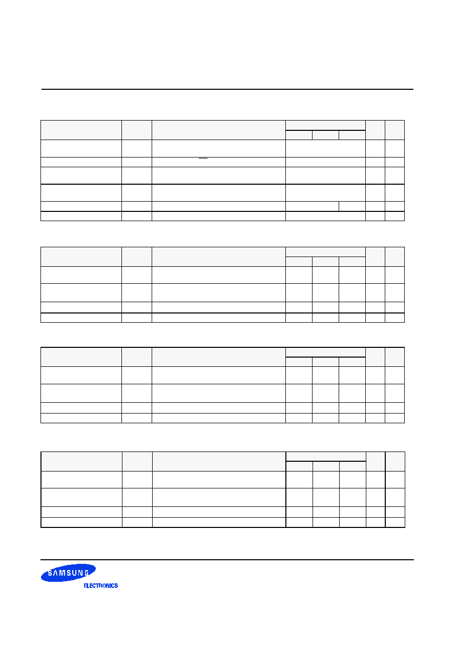
- 40 of 60 -
REV. 0.0 Apr. '99
PC 200/266 DDR SDRAM
128Mb DDR SDRAM
Table 12. DC specifications
Parameter
Symbol
Test Condition
Version
Unit
Note
-Z
-Y
-0
Precharge Power-down
Standby Current
IDD2P
CKE
VIL(max), tCK=tCK(min), All banks idle
25
mA
Idle Standby Current
IDD2N
CKE
VIH(min), CS
VIH(min), tCK=tCK(min)
45
mA
Active Power-down
Standby Current
IDD3P
All banks idle, CKE
VIL(max), tCK=tCK(min)
40
mA
Active Standby Current
IDD3N
One bank; Active-Precharge, tRC=tRAS(max),
tCK=tCK(min)
60
mA
Auto Refresh Current
IDD5
tRC
=
tRFC(min)
200
165
mA
2
Self Refresh Current
IDD6
CKE
0.2V
2.5
mA
Parameter
Symbol
Test Condition
Version
Unit
Note
-Z
-Y
-0
Operating Current
(One Bank Active)
IDD0
tRC
=
tRC(min) tCK=tCK(min)
Active-Precharge
T.B.D
T.B.D
T.B.D
mA
1
Operating Current
(One Bank Active)
IDD1
Burst=2 tRC
=
tRC(min), CL=2.5
I
OUT
=0mA, Active-Read-Precharge
135
135
115
mA
Operating Current(Read)
IDD4R
Burst=2, CL=2.5, tCK=tCK(min), I
OUT
=0mA
170
170
145
mA
1
Operating Current(Write)
IDD4W
Burst=2, CL=2.5, tCK=tCK(min)
130
130
110
mA
1
Parameter
Symbol
Test Condition
Version
Unit
Note
-Z
-Y
-0
Operating Current
(One Bank Active)
IDD0
tRC
=
tRC(min) tCK=tCK(min)
Active-Precharge
T.B.D
T.B.D
T.B.D
mA
1
Operating Current
(One Bank Active)
IDD1
Burst=2 tRC
=
tRC(min), CL=2.5
I
OUT
=0mA, Active-Read-Precharge
125
125
105
mA
Operating Current(Read)
IDD4R
Burst=2, CL=2.5, tCK=tCK(min), I
OUT
=0mA
150
150
125
mA
1
Operating Current(Write)
IDD4W
Burst=2, CL=2.5, tCK=tCK(min)
115
115
95
mA
1
16Mx8
128Mb(Common)
Note 1.Measured with outputs open.
2. Refresh period is 64ms.
Parameter
Symbol
Test Condition
Version
Unit
Note
-Z
-Y
-0
Operating Current
(One Bank Active)
IDD0
tRC
=
tRC(min) tCK=tCK(min)
Active-Precharge
T.B.D
T.B.D
T.B.D
mA
1
Operating Current
(One Bank Active)
IDD1
Burst=2 tRC
=
tRC(min), CL=2.5
I
OUT
=0mA, Active-Read-Precharge
145
140
125
mA
Operating Current(Read)
IDD4R
Burst=2, CL=2.5, tCK=tCK(min), I
OUT
=0mA
200
200
175
mA
1
Operating Current(Write)
IDD4W
Burst=2, CL=2.5, tCK=tCK(min)
150
150
130
mA
1
8Mx16
7.1 DC Specifications
32Mx4
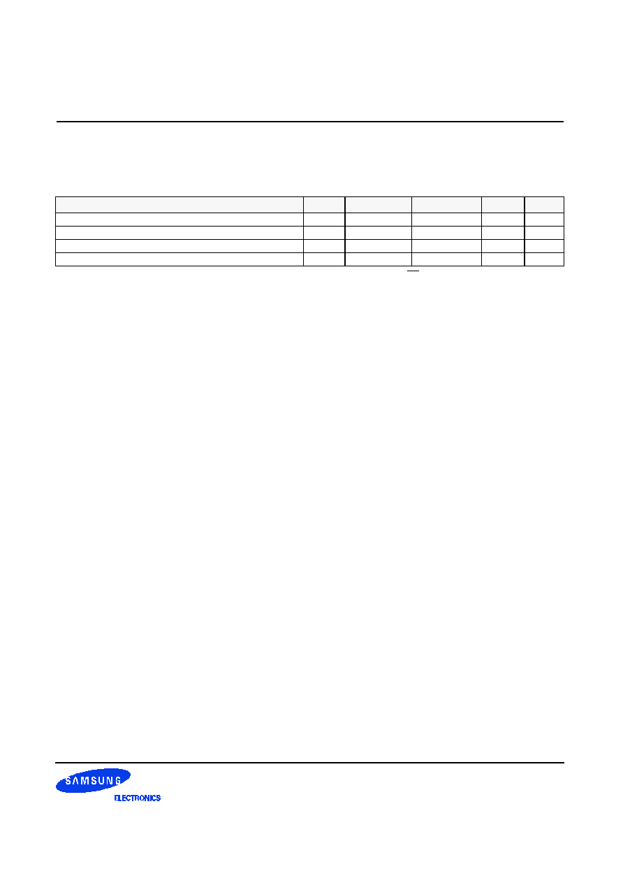
- 41 of 63 -
REV. 0.61 August 9. '99
128Mb DDR SDRAM
Target
8. AC Operating Conditions & Timming Specification
8.1 AC Operating Conditions
Parameter/Condition
Symbol
Min
Max
Unit
Note
Input High (Logic 1) Voltage, DQ, DQS and DM signals
VIH(AC)
VREF + 0.35
V
Input Low (Logic 0) Voltage, DQ, DQS and DM signals.
VIL(AC)
VREF - 0.35
V
Input Differential Voltage, CK and CK inputs
VID(AC)
0.7
VDDQ+0.6
V
1
Input Crossing Point Voltage, CK and CK inputs
VIX(AC)
0.5*VDDQ-0.2
0.5*VDDQ+0.2
V
2
Note 1. VID is the magnitude of the difference between the input level on CK and the input on CK.
2. The value of V
IX
is expected to equal 0.5*V
DDQ
of the transmitting device and must track variations in the DC level of the same.
Table 13. AC operating conditions
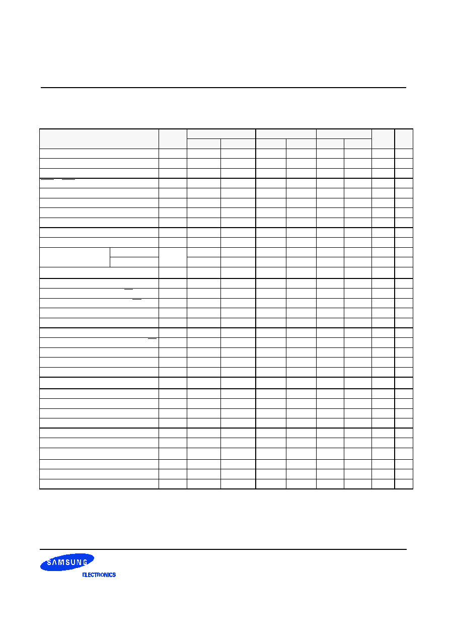
- 42 of 63 -
REV. 0.61 August 9. '99
128Mb DDR SDRAM
Target
Parameter
Symbol
- Z(PC266@CL=2)
- Y(PC266@CL=2.5) - 0(PC200@CL=2)
Unit
Note
Min
Max
Min
Max
Min
Max
Row cycle time
tRC
65
65
70
ns
Refresh row cycle time
tRFC
75
75
80
ns
Row active time
tRAS
45
12K
48
12K
48
12K
ns
RAS to CAS delay
tRCD
20
20
20
ns
Row precharge time
tRP
20
20
20
ns
Row active to Row active delay
tRRD
15
15
15
ns
Write recovery time
tWR
2
2
2
tCK
Last data in to Read command
tCDLR
1
1
1
tCK
Last data in to Write command
tCDLW
0
0
0
tCK
Col. address to Col. address delay
tCCD
1
1
1
tCK
Clock cycle time
CL=2.0
tCK
7.5
15
10
15
10
15
ns
CL=2.5
7
15
7.5
15
8
15
ns
Clock high level width
tCH
0.45
0.55
0.45
0.55
0.45
0.55
tCK
Clock low level width
tCL
0.45
0.55
0.45
0.55
0.45
0.55
tCK
DQS-out access time from CK/CK
tDQSCK
-0.75
+0.75
-0.75
+0.75
-0.8
+0.8
ns
Output data access time from CK/CK
tAC
-0.75
+0.75
-0.75
+0.75
-0.8
+0.8
ns
Data strobe edge to ouput data edge
tDQSQ
-0.5
+0.5
-0.5
+0.5
-0.6
+0.6
ns
Read Preamble
tRPRE
0.9
1.1
0.9
1.1
0.9
1.1
tCK
Read Postamble
tRPST
0.4
0.6
0.4
0.6
0.4
0.6
tCK
Data out high impedence time from CK/CK tHZQ
-0.75
+0.75
-0.75
+0.75
-0.8
+0.8
ns
2
CK to valid DQS-in
tDQSS
0.75
1.25
0.75
1.25
0.75
1.25
tCK
DQS-in setup time
tWPRES
0
0
0
ns
3
DQS-in hold time
tWPREH
0.25
0.25
0.25
tCK
DQS-in high level width
tDQSH
0.4
0.6
0.4
0.6
0.4
0.6
tCK
DQS-in low level width
tDQSL
0.4
0.6
0.4
0.6
0.4
0.6
tCK
DQS-in cycle time
tDSC
0.9
1.1
0.9
1.1
0.9
1.1
tCK
Address and Control Input setup time
tIS
1.1
1.1
1.2
ns
Address and Control Input hold time
tIH
1.1
1.1
1.2
ns
Mode register set cycle time
tMRD
15
15
16
ns
DQ & DM setup time to DQS
tDS
0.5
0.5
0.6
ns
DQ & DM hold time to DQS
tDH
0.5
0.5
0.6
ns
DQ & DM input pulse width
tDIPW
1.75
1.75
2
ns
Power down exit time
tPDEX
10
10
10
ns
Exit self refresh to write command
tXSW
95
116
ns
8.2 AC Timming Parameters & Specifications
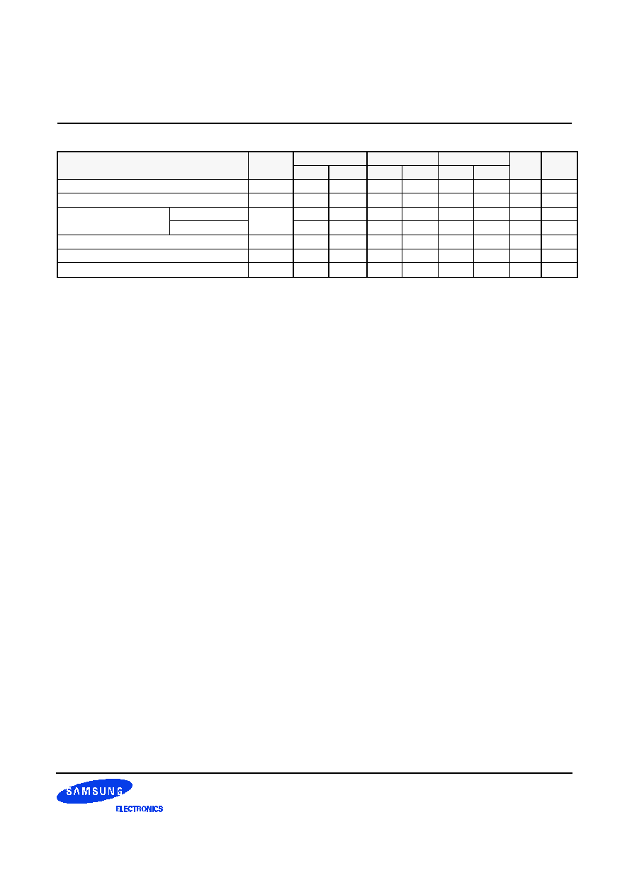
- 43 of 63 -
REV. 0.61 August 9. '99
128Mb DDR SDRAM
Target
.
1. Maximum burst refresh of 8
2. tHZQ transitions occurs in the same access time windows as valid data transitions. These parameters are not referenced
to a specific voltage level, but specify when the device output is no longer driving.
3. The specific requirement is that DQS be valid(High or Low) on or before this CK edge. The case shown(DQS going from
High_Z to logic Low) applies when no writes were previously in progress on the bus. If a previous write was in progress,
DQS could be High at this time, depending on tDQSS.
4. The maximum limit for this parameter is not a device limit. The device will operate with a great value for this parameter,
but system performance (bus turnaround) will degrade accordingly.
Parameter
Symbol
PC266A
PC266B
PC200
Unit
Note
Min
Max
Min
Max
Min
Max
Exit self refresh to bank active command
tXSA
75
75
80
ns
Exit self refresh to read command
tXSR
200
200
200
Cycle
Refresh interval time
64Mb, 128Mb
tREF
15.6
15.6
15.6
us
1
256Mb
7.8
7.8
7.8
us
1
Output DQS valid window
tDV
0.35
0.35
0.35
tCK
DQS write postamble time
tWPST
0.25
0.25
0.25
tCK
4
Auto precharge write recovery + Precharge time
tDAL
35
35
35
ns
Table 14. AC timing parameters and specifications

- 44 of 63 -
REV. 0.61 August 9. '99
128Mb DDR SDRAM
Target
9. AC Operating Test Conditions
(V
DD
=2.5/3.3V, V
DDQ
=2.5V, T
A
= 0 to 70
�
C)
Parameter
Value
Unit
Note
Input reference voltage for Clock
0.5 * V
DDQ
V
Input signal maximum peak swing
1.5
V
Input signal minimum slew rate
1.0
V/ns
Input Levels(V
IH
/V
IL
)
V
REF
+0.35/V
REF
-0.35
V
Input timing measurement reference level
V
REF
V
Output timing measurement reference level
V
tt
V
Output load condition
See Load Circuit
10. Input/Output Capacitance
(V
DD
=2.5, V
DDQ
=2.5V, T
A
= 25
�
C
,
f=1MHz)
Parameter
Symbol
Min
Max
Unit
Input capacitance
(A
0
~ A
11
, BA
0
~ BA
1,
CKE, CS, RAS,CAS, WE)
C
IN1
2.5
3.5
pF
Input capacitance(
CK, CK )
C
IN2
2.5
3.5
pF
Data & DQS input/output capacitance(DQ
0
~DQ
15
)
C
OUT
4.0
5.5
pF
Input capacitance(DM)
C
IN3
4.0
5.5
pF
Table 15. AC operating test conditions
Table 16. Input/output capacitance
Figure 24. Output Load Circuit (SSTL_2)
Output
Z0=50
C
LOAD
=30pF
V
REF
=0.5*V
DDQ
R
T
=50
V
tt
=0.5*V
DDQ

- 45 of 63 -
REV. 0.61 August 9. '99
128Mb DDR SDRAM
Target
11. IBIS: I/V Characteristics for Input and Output Buffers
1. The nominal pulldown V-I curve for DDR SDRAM devices will be within the inner bounding lines of the V-I
curve of Figure a.
2. The full variation in driver pulldown current from minimum to maximum process, temperature and voltage
will lie within the outer bounding lines the of the V-I curve of below Figure.
Maximum
Nominal High
Nominal Low
Minumum
Vout(V)
I
o
u
t
(
m
A
)
3. The nominal pullup V-I curve for DDR SDRAM devices will be within the inner bounding lines of the V-I
curve of below Figure.
4. The Full variation in driver pullup current from minimum to maximum process, temperature and voltage
will lie within the outer bounding lines of the V-I curve of below Figrue
Vout(V)
I
o
u
t
(
m
A
)
5. The full variation in the ratio of the maximum to minimum pullup and pulldown current will not exceed 1.7,
for device drain to source voltage from 0 to VDDQ/2
6. The Full variation in the ratio of the nominal pullup to pulldown current should be unity �10%, for device
drain to source voltages from 0 to VDDQ/2
Minimum
Nominal Low
Nominal High
Maximum
Figure 25. I/V characteristics for input/output buffers:Pull up(above) and pull down(below)
11.1 Normal strength driver
- 46 of 63 -
REV. 0.61 August 9. '99
128Mb DDR SDRAM
Target
Temperature (Tjunction)
Typical 50
�
C
Minimum 0
�
C
Maximum 0
�
C
Vdd/Vddq
Normal 2.5V
Minimum 2.3V
Maximum 2.7V
The adove characteristics are specied under best, worst and normal process variation/conditions
Pulldown Current (mA)
pullup Current (mA)
Voltage
(V)
Normal
Low
Normal
High
Minimum
Maximum
Normal
Low
Normal
High
Minimum
Maximum
0.1
5.7
6.4
4.3
8.3
-5.8
-7.2
-4.3
-8.6
0.2
11.5
12.7
8.7
16.5
-11.5
-13.7
-8.7
-17.0
0.3
17.1
19.0
13.0
24.4
-17.1
-20.0
-13.0
-25.3
0.4
22.7
25.1
17.4
32.0
-22.6
-26.1
-17.4
-33.6
0.5
28.1
31.1
21.7
39.4
-28.1
-32.2
-21.7
-41.7
0.6
32.6
36.9
26.1
46.6
-32.4
-38.2
-26.1
-49.6
0.7
37.2
41.7
30.4
53.6
-35.9
-44.2
-30.4
-57.5
0.8
41.2
47.0
34.7
59.6
-38.8
-50.1
-34.0
-65.2
0.9
44.8
52.1
37.4
65.9
-41.3
-56.0
-36.0
-72.9
1.0
48.4
56.9
40.2
72.0
-43.4
-61.8
-36.5
-80.4
1.1
51.0
61.5
42.3
77.8
-45.1
-67.5
-36.8
-87.7
1.2
53.0
65.9
43.6
83.3
-46.4
-73.2
-37.0
-94.9
1.3
54.6
70.0
44.4
88.5
-47.2
-78.9
-37.2
-102.0
1.4
55.9
74.0
44.7
93.5
-47.6
-84.6
-37.4
-109.0
1.5
56.7
77.6
45.0
97.9
-47.8
-90.1
-37.6
-116.0
1.6
57.1
81.0
45.3
102.3
-48.1
-95.6
-37.8
-123.0
1.7
57.5
84.1
45.7
105.8
-48.2
-101.0
-37.9
-129.0
1.8
58.0
87.0
46.1
109.3
-48.4
-106.0
-38.0
-136.0
1.9
58.5
89.9
46.3
112.8
-48.6
-112.0
-38.1
-142.0
2.0
59.0
91.7
46.6
116.3
-48.7
-117.0
-38.2
-148.0
2.1
59.3
93.5
46.8
119.3
-48.9
-122.0
-38.3
-154.0
2.2
59.7
95.2
47.0
122.2
-49.1
-127.0
-38.4
-160.0
2.3
60.2
96.1
47.1
124.9
-49.2
-132.0
-38.5
-166.0
2.4
60.5
97.0
47.2
127.4
-49.3
-137.0
-38.6
-171.0
2.5
60.9
97.9
47.4
129.5
-49.5
-142.0
-38.7
-177.0
Table 17. Pull down and pull up current values

- 47 of 63 -
REV. 0.61 August 9. '99
128Mb DDR SDRAM
Target
11.2 Half Strength Driver
THe half strength driver IBIS will be included in the
future.
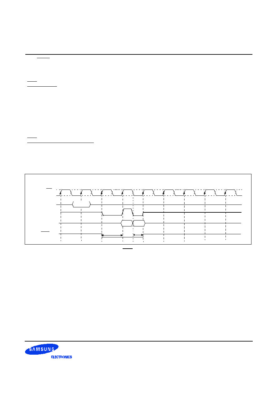
- 48 of 63 -
REV. 0.61 August 9. '99
128Mb DDR SDRAM
Target
12. QFC function
when drive low on reads coincident with the start of DQS, this DRAM output signal says that one cycle later
there will be the first valid DQS output and returned to HI-Z after this finishing a burst operation. It is also
driven low shortly after a write command is received and returned to HI-Z shortly after the last data strobe
transition is received. Whenever the device is in standby, the signal is HI-Z. DQS is intended to enable an
external data switch. QFC can be enabled or disabled through EMRS control
.
QFC timming on Read operation
QFC on reads is enabled coincident with the start of DQS preamble, and disabled coincident with the end of
DQS postamble
Command
2
0
1
5
3
4
8
6
7
Read
Dout 0 Dout 1
Hi-Z
DQS
DQ'S
QFC
t
QCS
t
QCH
CL = 2, BL = 2
CK
CK
QFC definition
Figure 26. QFC timing on read operation
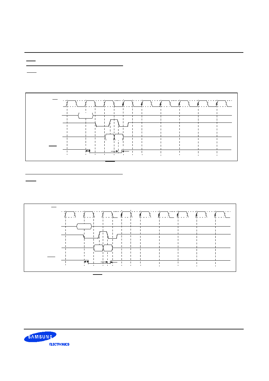
- 49 of 63 -
REV. 0.61 August 9. '99
128Mb DDR SDRAM
Target
QFC timming on Write operation with tDQSSmax
QFC on writes is enabled as soon as possible after the clock edge of write command and disabled as soon
as possible after the last DQS-in low going edge.
2
0
1
5
3
4
8
6
7
Hi-Z
DQS@tDQSSmax
QFC
t
QCSW
t
QCHW
Dout 0 Dout 1
BL = 2
Write
DQ'S@tDQSSmax
Command
CK
CK
QFC Timming on Write operation with tDQSSmin
DQS@tDQSSmin
DQ'S@tDQSSmin
QFC on writes is enabled as soon as possible after the clock edge of write command and disabled
as soon as possible after the last DQS-in low going edge.
2
0
1
5
3
4
8
6
7
Hi-Z
QFC
t
QCSW
t
QCHW
Dout 0 Dout 1
BL = 2
Write
Command
CK
CK
Figure 27. : QFC timing on write operation with tDQSSmax
Figure 28. : QFC timing on write operation with tDQSSmax