
KM416RD8AS
Direct RDRAM
TM
Target
Rev. 0.9 July 1999
KM 4 XX XX XX X X - X X XX
1
2
3
4
5
6
7
8
SAMSUNG Memory
Device
Organization
Product
Speed
Package Type
Revision
Density
1. SAMSUNG Memory
2. Device
3. Organization
4. Product
6. Revision
7. Package Type
10. Speed
5. Density
9
9. t
RAC
(Row Access Time)
t
RAC
(Row Access Time)
8. Power & Refresh
10
Power & Refresh
ORDERING INFORMATION
- 4 : DRAM
- 16 : x16 bit
- 18 : x18 bit
- RD : Direct RAMBUS DRAM
- 2 : 2M
- 4 : 4M
- 8 : 8M
- 16 : 16M
- Blank : 1st Gen.
- A : 2nd Gen.
- C : u - BGA(CSP-Forward)
- D : u - BGA(CSP-Reverse)
- W : WL - CSP
- S : u-BGA For Consumer Package
- Blank : Normal Power Self Refesh(32m/8K, 3.9us)
- L : Low Power Self Refesh(32m/8K, 3.9us)
- R : Normal Power Self Refesh(32m/16K, 1.9us)
- S : Low Power Self Refesh(32m/16K, 1.9us)
- DS : for Daisy Chain Sample
- 80 : 800Mbps (400MHz)
- 70 : 711Mbps (356MHz)
- 60 : 600Mbps (300MHz)
- Blank : for Daisy Chain Sample
- M : 40ns
- K : 45ns
- G : 53.3ns
- B~D, F, J, L, N~ : Reserved

Rev. 0.9 July 1999
Page 1
KM416RD8AS
Direct RDRAM
TM
Target
Overview
The Rambus Direct RDRAM
TM
is a general purpose high-
performance memory device suitable for use in a broad
range of applications including computer memory, graphics,
video, and any other application where high bandwidth and
low latency are required.
The 128Mbit Direct Rambus DRAMs (RDRAM
Æ
) ar
extremely high-speed CMOS DRAMs organized as 8M
words by 16 bits. The use of Rambus Signaling Level (RSL)
technology permits 800MHz transfer rates while using
conventional system and board design technologies. Direct
RDRAM devices are capable of sustained data transfers at
1.25 ns per two bytes (10ns per sixteen bytes).
The architecture of the Direct RDRAMs allows the highest
sustained bandwidth for multiple, simultaneous randomly
addressed memory transactions. The separate control and
data buses with independent row and column control yield
over 95% bus efficiency. The Direct RDRAM's thirty-two
banks support up to four simultaneous transactions.
System oriented features for mobile, graphics and large
memory systems include power management, byte masking.
Features
Highest sustained bandwidth per DRAM device
- 1.6GB/s sustained data transfer rate
- Separate control and data buses for maximized
efficiency
- Separate row and column control buses for
easy scheduling and highest performance
- 32 banks: four transactions can take place simul-
taneously at full bandwidth data rates
Low latency features
- Write buffer to reduce read latency
- 3 precharge mechanisms for controller flexibility
- Interleaved transactions
Advanced power management:
- Multiple low power states allows flexibility in power-
consumption versus time to transition to active state
- Power-down self-refresh
Organization: 1Kbyte pages and 32 banks, x 16
Uses Rambus Signaling Level (RSL) for up to 800MHz
operation
The 128Mbit Direct RDRAMs are offered in a CSP hori-
zontal package suitable for desktop as well as low-profile
add-in card and mobile applications.
Direct RDRAMs operate from a 2.5 volt supply.
Key Timing Parameters/Part Numbers
a.The
"
32s
"
designation indicates that this RDRAM core is composed of 32
banks which use a
"
split
"
bank architecture.
b.The
"
R
"
designation indicates that this RDRAM core uses Normal Power
Self Refresh.
c.The
"
S
"
designation indicates that this RDRAM core uses Low Power Self
Refresh.
Figure 1: Direct RDRAM Consumer CSP Package
Organization
Speed
Part Number
Binning
I/O
Freq.
MHz
t
rac
(Row
Access
Time) ns
256Kx16x32s
a
-RM80
800
40
KM416RD8AS-R
b
M80
-SM80
800
40
KM416RD8AS-S
c
M80
SEC KOREA
KM4
xx
RD8AC
SEC KOREA
KM416RD8AS-RK80
Page 2
KM416RD8AS
Direct RDRAM
TM
Target
Rev. 0.9 July 1999
S E C K O R E A
K M 4
x x
R D 8 A C
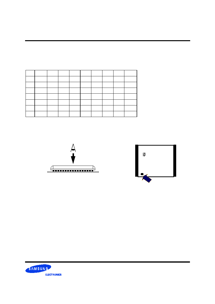
Pinouts and Definitions
This table shows the pin assignments of the center-bonded-
forward RDRAM package from the top-side of the package
(the view looking down on the package as it is mounted on
the circuit board).
Table 1 : Pin Assignment (Top View)
7
DQA7
DQA4
CFM
CFMN
RQ5
RQ3
DQB0
DQB4
DQB7
6
VSS
DQA5
DQA2
VDDA
RQ6
RQ2
DQB1
DQB5
VSS
5
CMD
VDD
VSS
VSSA
VDD
VSS
VDD
VDD
SIO0
4
3
SCK
VSS
VDD
VSS
VSS
VDD
VSS
VSS
SIO1
2
VCMOS
DQA6
DQA1
VREF
RQ7
RQ1
DQB2
DQB6
VCMOS
1
NC
DQA3
DQA0
CTMN
CTM
RQ4
RQ0
DQB3
NC
A
B
C
D
E
F
G
H
J
Chip
Top View
Top marking
example of Consumer package
For Consumer package, pin #1(ROW 1, COL A)
is located at the A1 postion on the top side and the
A1 position is marked by the marker
"
∑
"
SEC KOREA
KM416RD8AS-RK80

