 | –≠–ª–µ–∫—Ç—Ä–æ–Ω–Ω—ã–π –∫–æ–º–ø–æ–Ω–µ–Ω—Ç: KM6164002 | –°–∫–∞—á–∞—Ç—å:  PDF PDF  ZIP ZIP |

KM6164002, KM6164002E, KM6164002I
CMOS SRAM
PRELIMINARY
Rev 2.0
- 9 -
June -1997
PACKAGE DIMENSIONS
Units : Inches (millimeters)
#1
44-SOJ-400
#44
25.58
±
0.12
1.125
±
0.005
MAX
28.98
1.141
MAX
0.148
3.76
1.19
( )
0.047
1.27
( )
0.050
0.95
( )
0.0375
+0.10
0.43
-0.05
+0.004
0.017
-0.002
+0.10
0.71
-0.05
+0.004
0.028
-0.002
1.27
0.050
11.18
±
0.12
0.440
±
0.005
1
0
.
1
6
0
.
4
0
0
+0.10
0.20
-0.05
+0.004
0.008
-0.002
9.40
±
0.25
0.370
±
0.010
MIN
0.69
0.027
#22
#23
0.004
0.10 MAX

KM6164002, KM6164002E, KM6164002I
CMOS SRAM
PRELIMINARY
Rev 2.0
- 8 -
June -1997
TIMING WAVE FORM OF WRITE CYCLE(4)
(UB, LB Controlled)
CS
Data In
WE
High-Z
ADD
Data Out
Data Valid
High-Z(8)
UB, LB
High-Z
NOTES(WRITE CYCLE)
1. All write cycle timing is referenced from the last valid address to the first transition address.
2. A write occurs during the overlap of a low CS,WE,LB and UB. A write begins at the latest transition CS going low and WE going low ; A write ends at
the earliest transition CS going high or WE going high. t
WP
is measured from the beginning of write to the end of write.
3. t
CW
is measured from the later of CS going low to end of write.
4. t
AS
is measured from the address valid to the beginning of write.
5. t
WR
is measured from the end of write to the address change. t
WR
applied in case a write ends as CS, or WE going high.
6. If OE. CS and WE are in the Read Mode during this period, the I/O pins are in the output low-Z state. Inputs of opposite phase of the output mus t not
be applied because bus contention can occur.
7. For common I/O applications, minimization or elimination of bus contention conditions is necessary during read and write cycl e.
8. If CS goes low simultaneously with WE going or after WE going low, the outputs remain high impedance state.
9. Dout is the read data of the new address.
10. When CS is low : I/O pins are in the output state. The input signals in the opposite phase leading to the output should not be applied.
FUNCTIONAL DESCRIPTION
* NOTE : X means Don't Care.
CS
WE
OE
LB
UB
Mode
I/O Pin
Supply Current
I/O
1
~I/O
8
I/O
9
~I/O
16
H
X
X*
X
X
Not Select
High-Z
High-Z
I
SB
, I
SB1
L
H
H
X
X
Output Disable
High-Z
High-Z
I
CC
L
X
X
H
H
L
H
L
L
H
Read
D
OUT
High-Z
I
CC
H
L
High-Z
D
OUT
L
L
D
OUT
D
OUT
L
L
X
L
H
Write
D
IN
High-Z
I
CC
H
L
High-Z
D
IN
L
L
D
IN
D
IN
t
WC
t
AW
t
WP(2)
t
BW
t
CW(3)
t
AS(4)
t
WHZ(6)
t
DW
t
DH
t
BLZ
t
WR(5)
KM6164002, KM6164002E, KM6164002I
CMOS SRAM
PRELIMINARY
Rev 2.0
- 7 -
June -1997
TIMING WAVE FORM OF WRITE CYCLE(3)
(CS=Controlled)
CS
Data In
WE
High-Z
ADD
Data Out
Data Valid
High-Z(8)
UB, LB
High-Z
TIMING WAVE FORM OF WRITE CYCLE(2)
(OE=Low Fixed)
CS
Data In
WE
High-Z
ADD
Data Out
Data Valid
High-Z
(10)
(9)
UB, LB
t
WC
t
AW
t
WP1(2)
t
BW
t
CW(3)
t
AS(4)
t
WHZ(6)
t
DW
t
DH
t
WC
t
AW
t
WP(2)
t
BW
t
CW(3)
t
AS(4)
t
WHZ(6)
t
DW
t
DH
t
OH
t
OW
t
LZ
t
WR(5)
t
WR(5)
KM6164002, KM6164002E, KM6164002I
CMOS SRAM
PRELIMINARY
Rev 2.0
- 6 -
June -1997
TIMING WAVE FORM OF READ CYCLE(2)
(WE=V
IH
)
CS
OE
Data Out
Data Valid
ADD
NOTES(READ CYCLE)
1. WE is high for read cycle.
2. All read cycle timing is referenced from the last valid address to the first transition address.
3. t
HZ
and t
OHZ
are defined as the time at which the outputs achieve the open circuit condition and are not referenced to V
OH
or V
OL
Levels.
4. At any given temperature and voltage condition, t
HZ
(Max.) is less than t
LZ
(Min.) both for a given device and from device to device.
5. Transition is measured
±
200
ß∆
from steady state voltage with Load(B). This parameter is sampled and not 100% tested.
6. Device is continuously selected with CS=V
IL.
7. Address valid prior to coincident with CS transition low.
8. For common I/O applications, minimization or elimination of bus contention conditions is necessary during read and write cycl e.
UB, LB
UB, LB
TIMING WAVE FORM OF WRITE CYCLE(1)
(OE=Clock)
OE
CS
Data In
WE
High-Z
ADD
Data Out
Data Valid
High-Z(8)
t
RC
t
AA
t
CO
t
BLZ(4,5)
t
OE
t
BA
t
OLZ
t
LZ(4,5)
t
HZ(3,4,5)
t
BHZ(3,4,5)
t
OHZ
t
OH
t
WC
t
AW
t
WP(2)
t
BW
t
CW(3)
t
AS(4)
t
OHZ(6)
t
DW
t
DH
t
WR(5)
KM6164002, KM6164002E, KM6164002I
CMOS SRAM
PRELIMINARY
Rev 2.0
- 5 -
June -1997
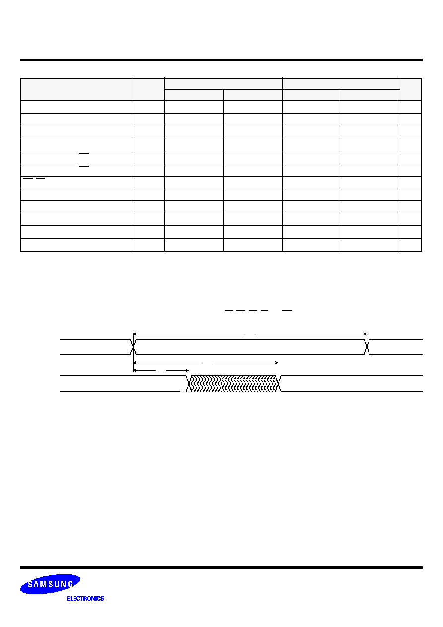
WRITE CYCLE
NOTE: Above parameters are also guaranteed at extended and industrial temperature ranges.
Parameter
Symbol
KM6164002-20
KM6164002-25
Unit
Min
Max
Min
Max
Write Cycle Time
t
WC
20
-
25
-
ß¿
Chip Select to End of Write
t
CW
15
-
17
-
ß¿
Address Set-up Time
t
AS
0
-
0
-
ß¿
Address Valid to End of Write
t
AW
15
-
17
-
ß¿
Write Pulse Width(OE High)
t
WP
15
-
17
-
ß¿
Write Pulse Width(OE Low)
t
WP1
20
-
25
-
ß¿
UB, LB Valid to End of Write
t
BW
15
-
17
-
ns
Write Recovery Time
t
WR
0
-
0
-
ß¿
Write to Output High-Z
t
WHZ
0
8
0
8
ß¿
Data to Write Time Overlap
t
DW
10
-
12
-
ß¿
Data Hold from Write Time
t
DH
0
-
0
-
ß¿
End Write to Output Low-Z
t
OW
3
-
4
-
ß¿
TIMING DIAGRAMS
TIMING WAVE FORM OF READ CYCLE(1)
(Address Controlled, CS=OE=UB=LB=V
IL
, WE=V
IH
)
ADD
Data Out
Previous Data Valid
Data Valid
t
RC
t
AA
t
OH