KM64V1003C
CMOS SRAM
Revision 1.0
- 1 -
Sep. 1998
Document Title
256Kx4 Bit (with OE) High Speed CMOS Static RAM(3.3V Operating)
Revision History
The attached data sheets are prepared and approved by SAMSUNG Electronics. SAMSUNG Electronics CO., LTD. reserve the right to change the
specifications. SAMSUNG Electronics will evaluate and reply to your requests and questions on the parameters of this device. If you have any ques-
tions, please contact the SAMSUNG branch office near your office, call or contact Headquarters.
Rev. No.
Rev. 0.0
Rev. 1.0
Remark
History
Initial Draft
Release to Final Data Sheet
1. Delete Preliminary
2. Relex DC characteristics
Item
Previous
Current
I
CC
12ns
65mA
70mA
15ns
63mA
68mA
20ns
60mA
65mA
Draft Data
Aug. 5. 1998
Sep. 7. 1998
Preliminary
Final
KM64V1003C
CMOS SRAM
Revision 1.0
- 2 -
Sep. 1998
256K x 4 Bit (with OE)High-Speed CMOS Static RAM(3.3V Operating)
GENERAL DESCRIPTION
FEATURES
� Fast Access Time 12,15,20ns(Max.)
� Low Power Dissipation
Standby (TTL) : 30mA(Max.)
(CMOS) : 5mA(Max.)
Operating KM64V1003C - 12 : 70mA(Max.)
KM64V1003C - 15 : 68mA(Max.)
KM64V1003C - 20 : 65mA(Max.)
� Single 3.3
�
0.3V Power Supply
� TTL Compatible Inputs and Outputs
� Fully Static Operation
- No Clock or Refresh required
� Three State Outputs
� Center Power/Ground Pin Configuration
� Standard Pin Configuration
KM64V1003CJ : 32-SOJ-400
The KM64V1003C is a 1,048,576-bit high-speed Static Ran-
dom Access Memory organized as 262,144 words by 4 bits.
The KM64V1003C uses 4 common input and output lines and
has an output enable pin which operates faster than address
access time at read cycle. The device is fabricated using SAM-
SUNG
s advanced CMOS process and designed for high-
speed circuit technology. It is particularly well suited for use in
high-density high-speed system applications. The
KM64V1003C is packaged in a 400 mil 32-pin plastic SOJ.
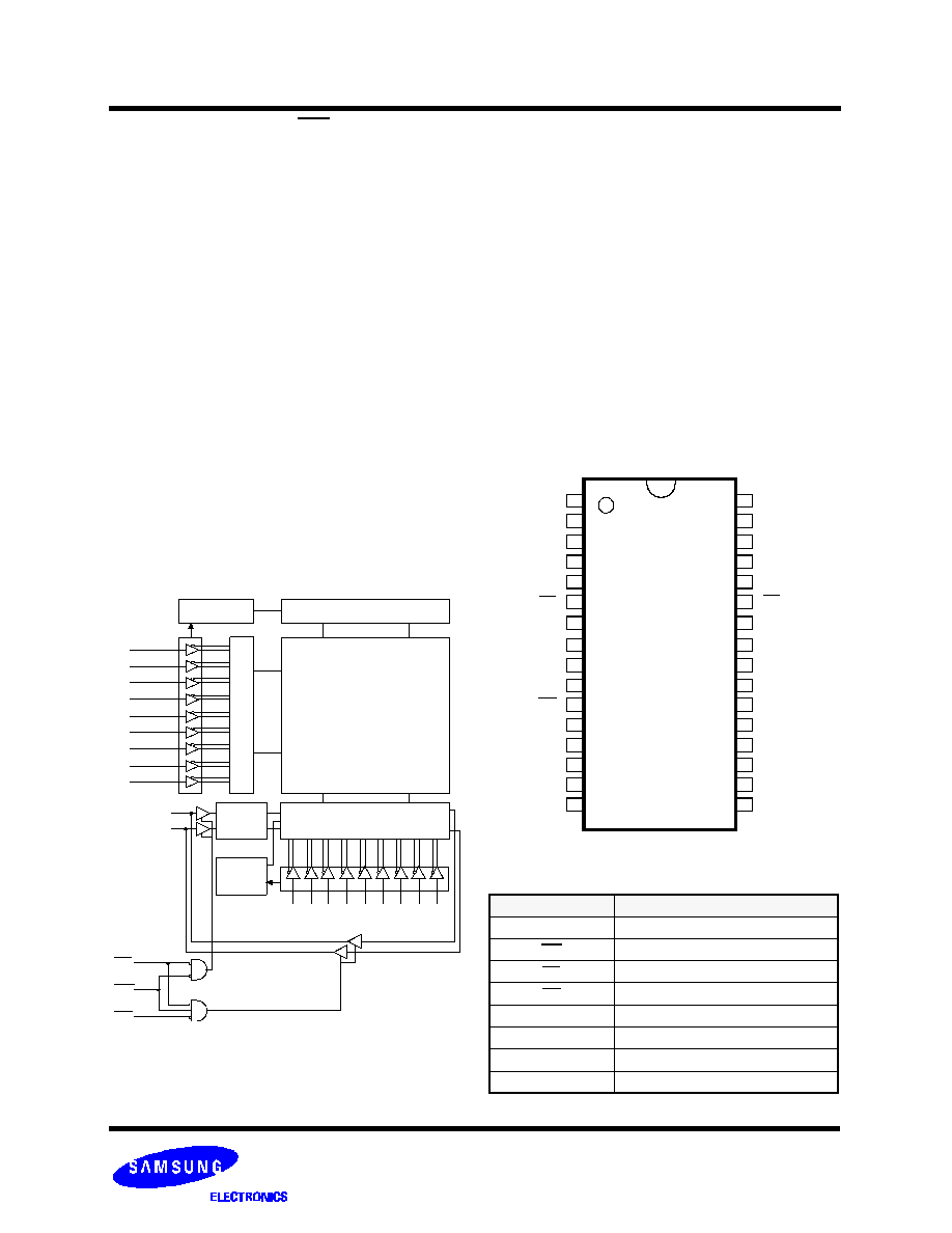
PIN FUNCTION
Pin Name
Pin Function
A
0
- A
17
Address Inputs
WE
Write Enable
CS
Chip Select
OE
Output Enable
I/O
1
~ I/O
4
Data Inputs/Outputs
V
CC
Power(+3.3V)
V
SS
Ground
N.C
No Connection
PIN CONFIGURATION
(Top View)
Clk Gen.
I/O
1
~I/O
4
CS
WE
OE
FUNCTIONAL BLOCK DIAGRAM
R
o
w
S
e
l
e
c
t
Data
Cont.
Column Select
CLK
Gen.
Pre-Charge Circuit
Memory Array
512 Rows
512x4 Columns
I/O Circuit &
SOJ
1
2
3
4
5
6
7
8
9
10
11
12
13
14
15
16
32
31
30
29
28
27
26
25
24
23
22
21
20
19
18
17
A
17
A
16
A
15
A
14
A
13
OE
I/O
4
Vss
Vcc
I/O
3
A
12
A
11
A
10
A
9
A
8
N.C.
N.C.
A
0
A
1
A
2
A
3
CS
I/O
1
Vcc
Vss
I/O
2
WE
A
4
A
5
A
6
A
7
N.C.
A
10
A
11
A
12
A
13
A
14
A
15
A
0
A
1
A
2
A
3
A
4
A
5
A
6
A
7
A
9
A
16
A
17
A
8
KM64V1003C
CMOS SRAM
Revision 1.0
- 3 -
Sep. 1998
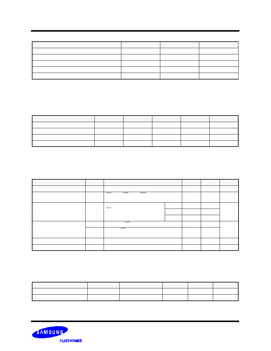
ABSOLUTE MAXIMUM RATINGS*
* Stresses greater than those listed under "Absolute Maximum Ratings" may cause permanent damage to the device. This is a stress ating only and
functional operation of the device at these or any other conditions above those indicated in the operating sections of this specification is not implied.
Exposure to absolute maximum rating conditions for extended periods may affect reliability.
Parameter
Symbol
Rating
Unit
Voltage on Any Pin Relative to V
SS
V
IN
,
V
OUT
-0.5 to 4.6
V
Voltage on V
CC
Supply Relative to V
SS
V
CC
-0.5 to 4.6
V
Power Dissipation
P
D
1
W
Storage Temperature
T
STG
-65 to 150
�
C
Operating Temperature
T
A
0 to 70
�
C
RECOMMENDED DC OPERATING CONDITIONS
(T
A
=0 to 70
�
C)
NOTE:* V
IL
(Min)=-2.0V a.c(Pulse Width
8ns) for I
20mA
** V
IH
(Max)=V
CC
+ 2.0V a.c (Pulse Width
8ns) for I
20mA
Parameter
Symbol
Min
Typ
Max
Unit
Supply Voltage
V
CC
3.0
3.3
3.6
V
Ground
V
SS
0
0
0
V
Input High Voltage
V
IH
2.0
-
V
CC
+ 0.5**
V
Input Low Voltage
V
IL
-0.5*
-
0.8
V
DC AND OPERATING CHARACTERISTICS
(T
A
=0 to 70
�
C, Vcc=3.3
�
0.3V, unless otherwise specified
)
Parameter
Symbol
Test Conditions
Min
Max
Unit
Input Leakage Current
I
LI
V
IN
=V
SS
to
V
CC
-2
2
�
A
Output Leakage Current
I
LO
CS=V
IH
or OE=V
IH
or WE=V
IL
V
OUT
=V
SS
to
V
CC
-2
2
�
A
Operating Current
I
CC
Min. Cycle, 100% Duty
CS=V
IL,
V
IN
=V
IH
or
V
IL,
I
OUT
=0mA
12ns
-
70
mA
15ns
-
68
20ns
-
65
Standby Current
I
SB
Min. Cycle, CS=V
IH
-
30
mA
I
SB1
f=0MHz, CS
V
CC
-0.2V,
V
IN
V
CC
-0.2V or V
IN
0.2V
-
5
Output Low Voltage Level
V
OL
I
OL
=8mA
-
0.4
V
Output High Voltage Level
V
OH
I
OH
=-4mA
2.4
-
V
CAPACITANCE*
(T
A
=25
�
C, f=1.0MHz)
* NOTE : Capacitance is sampled and not 100% tested.
Item
Symbol
Test Conditions
MIN
Max
Unit
Input/Output Capacitance
C
I/O
V
I/O
=0V
-
8
pF
Input Capacitance
C
IN
V
IN
=0V
-
6
pF
KM64V1003C
CMOS SRAM
Revision 1.0
- 4 -
Sep. 1998
READ CYCLE
Parameter
Symbol
KM64V1003C-12
KM64V1003C-15
KM64V1003C-20
Unit
Min
Max
Min
Max
Min
Max
Read Cycle Time
t
RC
12
-
15
-
20
-
ns
Address Access Time
t
AA
-
12
-
15
-
20
ns
Chip Select to Output
t
CO
-
12
-
15
-
20
ns
Output Enable to Valid Output
t
OE
-
6
-
7
-
9
ns
Chip Enable to Low-Z Output
t
LZ
3
-
3
-
3
-
ns
Output Enable to Low-Z Output
t
OLZ
0
-
0
-
0
-
ns
Chip Disable to High-Z Output
t
HZ
0
6
-
7
-
9
ns
Output Disable to High-Z Output
t
OHZ
0
6
-
7
-
9
ns
Output Hold from Address Change
t
OH
3
-
3
-
3
-
ns
Chip Selection to Power Up Time
t
PU
0
-
0
-
0
-
ns
Chip Selection to Power DownTime
t
PD
-
12
-
15
-
20
ns
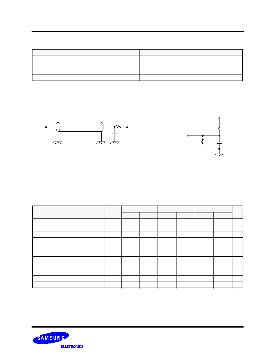
TEST CONDITIONS
Parameter
Value
Input Pulse Levels
0V to 3V
Input Rise and Fall Times
3ns
Input and Output timing Reference Levels
1.5V
Output Loads
See below
AC CHARACTERISTICS
(T
A
=0 to 70
�
C, V
CC
=3.3
�
0.3V, unless otherwise noted.)
Output Loads(B)
D
OUT
5pF*
319
353
for t
HZ
, t
LZ
, t
WHZ
, t
OW
, t
OLZ
& t
OHZ
+3.3V
* Including Scope and Jig Capacitance
Output Loads(A)
D
OUT
R
L
= 50
Z
O
= 50
V
L
= 1.5V
30pF*
* Capacitive Load consists of all components of the
test environment.
KM64V1003C
CMOS SRAM
Revision 1.0
- 5 -
Sep. 1998
WRITE CYCLE
Parameter
Symbol
KM64V1003C-12
KM64V1003C-15
KM64V1003C-20
Unit
Min
Max
Min
Max
Min
Max
Write Cycle Time
t
WC
12
-
15
-
20
-
ns
Chip Select to End of Write
t
CW
8
-
9
-
10
-
ns
Address Set-up Time
t
AS
0
-
0
-
0
-
ns
Address Valid to End of Write
t
AW
8
-
9
-
10
-
ns
Write Pulse Width(OE High)
t
WP
8
-
9
-
10
-
ns
Write Pulse Width(OE Low)
t
WP1
12
-
15
-
20
-
ns
Write Recovery Time
t
WR
0
-
0
-
0
-
ns
Write to Output High-Z
t
WHZ
0
6
0
7
0
9
ns
Data to Write Time Overlap
t
DW
6
-
7
-
8
-
ns
Data Hold from Write Time
t
DH
0
-
0
-
0
-
ns
End Write to Output Low-Z
t
OW
3
-
3
-
3
-
ns
Address
Data Out
Previous Valid Data
Valid Data
TIMMING DIAGRAMS
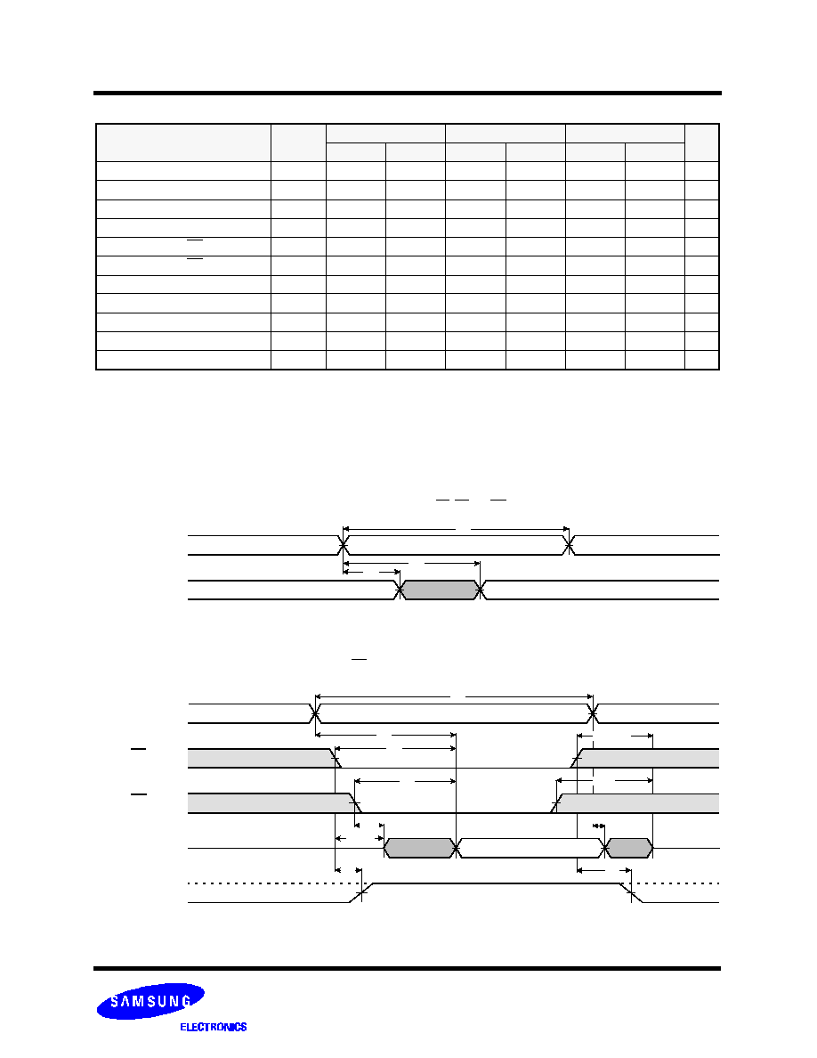
TIMING WAVEFORM OF READ CYCLE(1)
(Address Controlled
,
CS=OE=V
IL
, WE=V
IH
)
t
AA
t
RC
t
OH
TIMING WAVEFORM OF READ CYCLE(2)
(WE=V
IH
)
CS
Address
OE
Data out
t
AA
t
OLZ
t
LZ(4,5)
t
OH
t
OHZ
t
RC
t
OE
t
CO
t
PU
t
PD
t
HZ(3,4,5)
50%
50%
V
CC
Current
I
CC
I
SB
Valid Data