
PRELIMINARY
Revision 0.3
KM681000B Family
CMOS SRAM
April 1996
128K x8 bit Low Power CMOS Static RAM
The KM681000B family is fabricated by SAMSUNG's advanced
CMOS process technology. The family can support various
operating temperature ranges and have various package types
for user flexibility of system design. The family also support low
data retention voltage for battery back-up operation with low
data retention current.
GENERAL DESCRIPTION
FEATURES
°Ð
Process Technology : 0.6
ß-
CMOS
°Ð
Organization : 128Kx8
°Ð
Power Supply Voltage : Single 5.0V
°æ
10%
°Ð
Low Data Retention Voltage : 2V(Min)
°Ð
Three state output and TTL Compatible
°Ð
Package Type : JEDEC Standard
32-DIP, 32-SOP, 32-TSOP I R/F
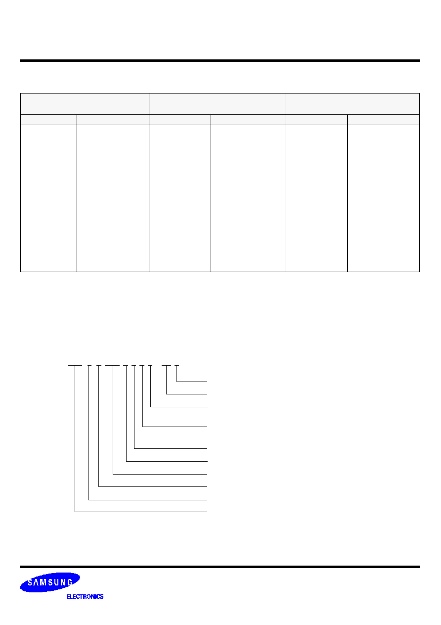
PIN DESCRIPTION
Name
Function
A
0
~A
16
Address Inputs
WE
Write Enable Input
CS
1
,CS
2
Chip Select Inputs
OE
Output Enable Input
I/O
1
~I/O
18
Data Inputs/Outputs
Vcc
Power
Vss
Ground
N.C
No Connection
X
-
D
e
c
o
d
e
r
Cell
Array
PRODUCT FAMILY
Product
Family
Operating
Temperature
Speed
PKG Type
Power Dissipation
Standby
(I
SB1
, Max)
Operating
(I
CC2
)
KM681000BL
Commercial(0~7
°…
)
55/70ns
32-DIP,32-SOP
32-TSOP I R/F
100
ßÀ
70mA
KM681000BL-L
20
ßÀ
KM681000BLE
Extended(-25~85
°…
)
70/100ns
32-SOP
32-TSOP I R/F
100
ßÀ
KM681000BLE-L
50
ßÀ
KM681000BLI
Industrial(-40~85
°…
)
70/100ns
32-SOP
32-TSOP I R/F
100
ßÀ
KM681000BLI-L
50
ßÀ
C
o
n
t
r
o
l
L
o
g
i
c
Y-Decoder
I/O Buffer
FUNCTIONAL BLOCK DIAGRAM
A
0~3,
A
8~11
A
4~7,
I/O
1
~
8
32-TSOP
Type I-Reverse
A
12~16
CS
1
,CS
2
WE
,
OE
A
11
A
9
A
8
A
13
WE
CS
2
A
15
V
CC
NC
A
16
A
14
A
12
A
7
A
6
A
5
A
4
OE
A
10
CS
1
I/O
8
I/O
7
I/O
6
I/O
5
I/O
4
V
SS
I/O
3
I/O
2
I/O
1
A
0
A
1
A
2
A
3
32-TSOP
Type I - Forward
32
31
30
29
28
27
26
25
24
23
22
21
20
19
18
17
1
2
3
4
5
6
7
8
9
10
11
12
13
14
15
16
N.C
A
16
A
14
A
12
A
7
A
6
A
5
A
4
A
3
A
2
A
1
A
0
I/O
1
I/O
2
I/O
3
V
SS
V
CC
A
15
CS
2
WE
A
13
A
8
A
9
A
11
OE
A
10
CS
1
I/O
8
I/O
7
I/O
6
I/O
5
I/O
4
32-DIP
32
31
30
29
28
27
26
25
24
23
22
21
20
19
18
17
1
2
3
4
5
6
7
8
9
10
11
12
13
14
15
16
32-SOP
A
11
A
9
A
8
A
13
WE
CS
2
A
15
V
CC
NC
A
16
A
14
A
12
A
7
A
6
A
5
A
4
OE
A
10
CS
1
I/O
8
I/O
7
I/O
6
I/O
5
I/O
4
V
SS
I/O
3
I/O
2
I/O
1
A
0
A
1
A
2
A
3
32
31
30
29
28
27
26
25
24
23
22
21
20
19
18
17
1
2
3
4
5
6
7
8
9
10
11
12
13
14
15
16
PRELIMINARY
Revision 0.3
KM681000B Family
CMOS SRAM
April 1996
PRODUCT LIST & ORDERING INFORMATION
PRODUCT LIST
Commercial Temp Product
(0~70
°…
)
Extended Temp Products
(-25~85
°…
)
Industrial Temp Products
(-40~85
°…
)
Part Name
Function
Part Name
Function
Part Name
Function
KM681000BLP-5
KM681000BLP-5L
KM681000BLP-7
KM681000BLP-7L
KM681000BLG-5
KM681000BLG-5L
KM681000BLG-7
KM681000BLG-7L
KM681000BLT-5
KM681000BLT-5L
KM681000BLT-7
KM681000BLT-7L
KM681000BLR-5
KM681000BLR-5L
KM681000BLR-7
KM681000BLR-7L
32-DIP,55ns,L-pwr
32-DIP,55ns,LL-pwr
32-DIP,70ns,L-pwr
32-DIP,70ns,LL-pwr
32-SOP,55ns,L-pwr
32-SOP,55ns,LL-pwr
32-SOP,70ns,L-pwr
32-SOP,70ns,LL-pwr
32-TSOP F,55ns,L-pwr
32-TSOP F,55ns,LL-pwr
32-TSOP F,70ns,L-pwr
32-TSOP F,70ns,LL-pwr
32-TSOP R,55ns,L-pwr
32-TSOP R,55ns,LL-pwr
32-TSOP R,70ns,L-pwr
32-TSOP R,70ns,LL-pwr
KM681000BLGE-7
KM681000BLGE-7L
KM681000BLGE-10
KM681000BLGE-10L
KM681000BLTE-7
KM681000BLTE-7L
KM681000BLTE-10
KM681000BLTE-10L
KM681000BLRE-7
KM681000BLRE-7L
KM681000BLRE-10
KM681000BLRE-10L
32-SOP,70ns,L-pwr
32-SOP,70ns,LL-pwr
32-SOP,100ns,L-pwr
32-SOP,100ns,LL-pwr
32-TSOP F,70ns,L-pwr
32-TSOP F,70ns,LL-pwr
32-TSOP F,100ns,L-pwr
32-TSOP F,100ns,LL-pwr
32-TSOP R,70ns,L-pwr
32-TSOP R,70ns,LL-pwr
32-TSOP R,100ns,L-pwr
32-TSOP R,100ns,LL-pwr
KM681000BLGI-7
KM681000BLGI-7L
KM681000BLGI-10
KM681000BLGI-10L
KM681000BLTI-7
KM681000BLTI-7L
KM681000BLTI-10
KM681000BLTI-10L
KM681000BLRI-7
KM681000BLRI-7L
KM681000BLRI-10
KM681000BLRI-10L
32-SOP,70ns,L-pwr
32-SOP,70ns,LL-pwr
32-SOP,100ns,L-pwr
32-SOP,100ns,LL-pwr
32-TSOP F,70ns,L-pwr
32-TSOP F,70ns,LL-pwr
32-TSOP F,100ns,L-pwr
32-TSOP F,100ns,LL-pwr
32-TSOP R,70ns,L-pwr
32-TSOP R,70ns,LL-pwr
32-TSOP R,100ns,L-pwr
32-TSOP R,100ns,LL-pwr
ORDERING INFORMATION
KM6 8 X 1000 B X X X - XX X
L-Low Low Power, Blank-Low Power or High Power
Access Time : 5=55ns, 7=70ns, 10=100ns
L-Low Power or Low Low Power, Blank-High Power
Die Version : B=3 rd generation
Density : 1000=1Mbit
Bank=5V, V=3.0~3.6V, U=2.7~3.3V
Organization : 8=x8
SEC Standard SRAM
¢•
Operating temperature : Blank=Commerial, I=Industrial, E=Extended,
Package Type : P-DIP, G=SOP, T=TSOP Forward, R=TSOP Reverse

PRELIMINARY
Revision 0.3
KM681000B Family
CMOS SRAM
April 1996
ABSOLUTE MAXIMUM RATINGS
*
* Stresses greater than those listed under "Absolute Maximum Ratings" may cause permanent damage to the device. This is a stres s rating only and functional operation of the
device at these or any other conditions above those indicated in the operating section of this specification is not implied. Exposure to absolute maximum rating conditions for
extended periods may affect reliability.
Item
Symbol
Ratings
Unit
Remark
Voltage on any pin relative to Vss
V
IN
,V
OUT
-0.5 to 7.0
V
-
Voltage on Vcc supply relative to Vss
V
CC
-0.5 to 7.0
V
-
Power Dissipation
P
D
1.0
W
-
Storage temperature
T
STG
-65 to 150
°…
-
Operating Temperature
T
A
0 to 70
°…
KM681000BL/L-L
-25 to 85
°…
KM681000BLE/LE-L
-40 to 85
°…
KM681000BLI/LI-L
Soldering temperature and time
T
SOLDER
260
°…
, 10sec (Lead Only)
-
-
RECOMMENDED DC OPERATING CONDITIONS
*
* 1) Commercial Product : T
A
=0 to 70
°…
, unless otherwise specified
2) Extended Product : T
A
=-25 to 85
°…
, unless otherwise specified
3) Industrial Product : T
A
=-40 to 85
°…
, unless otherwise specified
** T
A
=25
°…
*** V
IL
(min)=-3.0V for
°¬
50ns pulse width
Item
Symbol
Min
Typ**
Max
Unit
Supply voltage
Vcc
4.5
5.0
5.5
V
Ground
Vss
0
0
0
V
Input high voltage
V
IH
2.2
-
Vcc+0.5
V
Input low voltage
V
IL
-0.5***
-
0.8
V
CAPACITANCE*
(f=1MHz, T
A
=25
°…
)
* Capacitance is sampled not 100% tested
Item
Symbol
Test Condition
Min
Max
Unit
Input capacitance
C
IN
Vin=0V
-
6
pF
Input/Output capacitance
C
IO
Vio=0V
-
8
pF
PRELIMINARY
Revision 0.3
KM681000B Family
CMOS SRAM
April 1996
DC AND OPERATING CHARACTERISTICS
* 1) Commercial Product : T
A
=0 to 70
°…
, Vcc=5.0V
°æ
10%, unless otherwise specified
2) Extended Product : T
A
=-25 to 85
°…
, Vcc=5.0V
°æ
10%, unless otherwise specified
2) Industrial Product : T
A
=-40 to 85
°…
, Vcc=5.0V
°æ
10%, unless otherwise specified
** 20mA for Exteneded and Industrial Products
*** 15mA for Extended and Industrial Products
Item
Symbol
Test Conditions*
Mi
Typ**
Max
Unit
Input leakage current
I
LI
V
IN
=Vss to Vcc
-1
-
1
ßÀ
Output leakage current
I
LO
CS
1
=V
IH
or CS
2
=V
IL
or WE=V
IL,
V
IO=
V
ss
to V
cc
-1
-
1
ßÀ
Operating power supply current
I
CC
CS
1
=V
IL
, CS
2
=V
IH
, V
IN
=V
IH
or V
IL
, I
IO
=0mA
-
7
15**
mA
Average operating current
I
CC1
Cycle time=1
ß¡
100% duty
CS
1
°¬
0.2V, CS
2
°√
V
CC
-0.2V
-
-
10***
mA
I
CC2
I
IO
=0mA CS
1
=V
IL
,CS
2
=V
IH
Min cycle, 100% duty
-
-
70
mA
Output low voltage
V
OL
I
OL
=2.1mA
-
-
0.4
V
Output high voltage
V
OH
I
OH
=-1.0mA
2.4
-
-
V
Standby Current(TTL)
I
SB
CS
1
=V
IH,
CS
2
=V
IL
-
-
3
mA
Standby
Current (CMOS)
KM681000BL
KM681000BL-L
I
SB1
CS
1
°√
Vcc-0.2V
CS
2
°√
Vcc-0.2V or
CS
2
°¬
0.2V
Other input=0~Vcc
L (Low Power)
LL (Low Low Power)
-
-
-
-
100
20
ßÀ
ßÀ
KM681000BLE
KM681000BLE-L
L (Low Power)
LL (Low Low Power)
-
-
-
-
100
50
ßÀ
ßÀ
KM681000BLI
KM681000BLI-L
L (Low Power)
LL (Low Low Power)
-
-
-
-
100
50
ßÀ
ßÀ
TEST CONDITIONS
(1.Test Load and Test Input/Output Reference)*
* See DC Operating conditions
Item
Value
Remark
Input pulse level
0.8 to 2.4V
-
Input rising & falling time
5ns
-
input and output reference voltage
1.5V
-
Output load (See right)
C
L
=100pF+1TTL
-
A.C CHARACTERISTICS
C
L
*
* Including scope and jig capacitance
PRELIMINARY
Revision 0.3
KM681000B Family
CMOS SRAM
April 1996
TEST CONDITIONS
(2. Temperature and Vcc Conditions)
Product Family
Temperature
Power Supply(Vcc)
Speed Bin
Comments
KM681000BL/L-L
0~70
°…
5.0V
°æ
10%
55/70ns
Commercial
KM681000BLE/LE-L
-25~85
°…
5.0V
°æ
10%
70/100ns
Extended
KM681000BLI/LI-L
-40~85
°…
5.0V
°æ
10%
70/100ns
Industrial
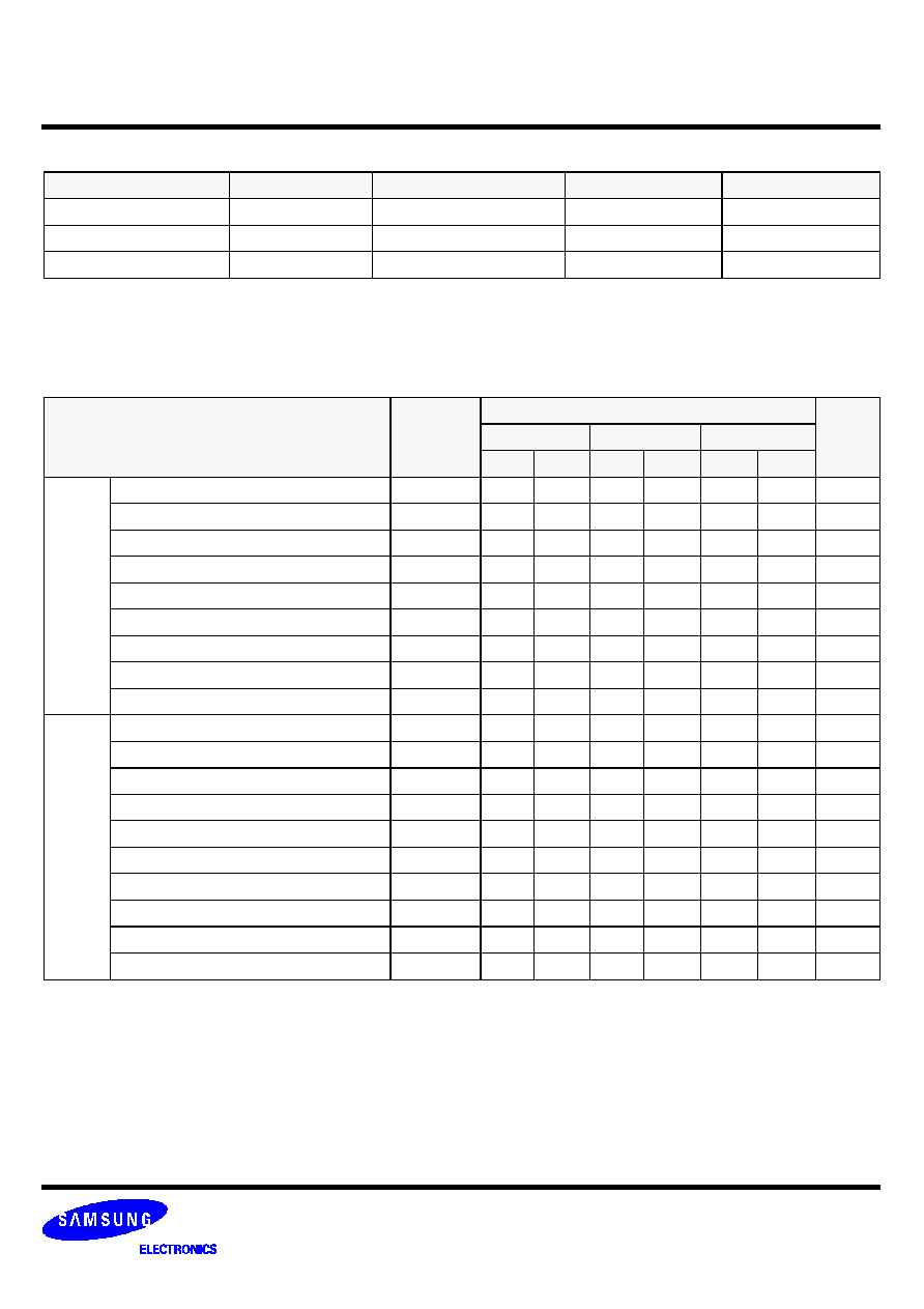
PARAMETER LIST FOR EACH SPEED BIN
Parameter List
Symbol
Speed Bins
Units
55ns
70ns
100ns
Min
Max
Min
Max
Min
Max
Read
Read cycle time
t
RC
55
-
70
-
100
-
ns
Address access time
t
AA
-
55
-
70
-
100
ns
Chip select to output
t
CO1,
t
CO2
-
55
-
70
-
100
ns
Output enable to valid output
t
OE
-
25
-
35
-
50
ns
Chip select to low-Z output
t
LZ1,
t
LZ2
10
-
10
-
10
-
ns
Output enable to low-Z output
t
OLZ
5
-
5
-
5
-
ns
Chip disable to high-Z output
t
HZ1,
t
HZ2
0
20
0
25
0
30
ns
Output disable to high-Z output
t
OHZ
0
20
0
25
0
30
ns
Output hold from address change
t
OH
10
-
10
-
10
-
ns
Write
Write cycle time
t
WC
55
-
70
-
100
-
ns
Chip select to end of write
t
CW
45
-
60
-
80
-
ns
Address set-up time
t
AS
0
-
0
-
0
-
ns
Address valid to end of write
t
AW
45
-
60
-
80
-
ns
Write pulse width
t
WP
40
-
50
-
60
-
ns
Write recovery time
t
WR
0
-
0
-
0
-
ns
Write to output high-Z
t
WHZ
0
20
0
25
0
30
ns
Data to write time overlap
t
DW
25
-
30
-
40
-
ns
Data hold from write time
t
DH
0
-
0
-
0
-
ns
End write to output low-Z
t
OW
5
-
5
-
5
-
ns