
KM68257C/CL
CMOS SRAM
PRELIMINARY
Rev 3.0
- 1 -
February-1996
Document Title
32Kx8 Bit High Speed Static RAM(5V Operating), Evolutionary Pin out.
Operated at Commercial Temperature Range.
Revision History
The attached data sheets are prepared and approved by SAMSUNG Electronics. SAMSUNG Electronics CO., LTD. reserve the right
to change the specifications. SAMSUNG Electronics will evaluate and reply to your requests and questions on the parameters of this
device. If you have any questions, please contact the SAMSUNG branch office near your office, call or contact Headquarters.
Rev No.
Rev. 0.0
Rev. 1.0
Rev. 2.0
Rev. 3.0
Remark
Preliminary
Final
Final
Final
History
Initial release with Preliminary.
Release to final Data Sheet.
1. Delete Preliminary
Update A.C parameters
2.1. Updated A.C parameters
2.2. Add Voh
1
=3.95V with the test condition as Vcc=5V
±
5% at 25
∞
C
3.1. Add 28-TSOP1 Package.
3.2. Add L-version.
3.3. Add Data Rentention Characteristics.
Items
Previous spec.
(12/15/20ns part)
Updated spec.
(12/15/20ns part)
t
OE
- / 8/10ns
- / 7 /9 ns
t
CW
- /12/ - ns
- /11/ - ns
t
HZ
8/10/10ns
6/7/8ns
t
OHZ
- / 8 / - ns
- / 7 / - ns
t
DW
- / 9 / - ns
- / 8 / - ns
Draft Data
Apr. 1st, 1994
May 14th,1994
Oct. 4th, 1994
Feb. 22th, 1996
KM68257C/CL
CMOS SRAM
PRELIMINARY
Rev 3.0
- 2 -
February-1996
PIN FUNCTION
Pin Name
Pin Function
A
0
- A
14
Address Inputs
WE
Write Enable
CS
Chip Select
OE
Output Enable
I/O
1
~ I/O
8
Data Inputs/Outputs
V
CC
Power(+5.0V)
V
SS
Ground
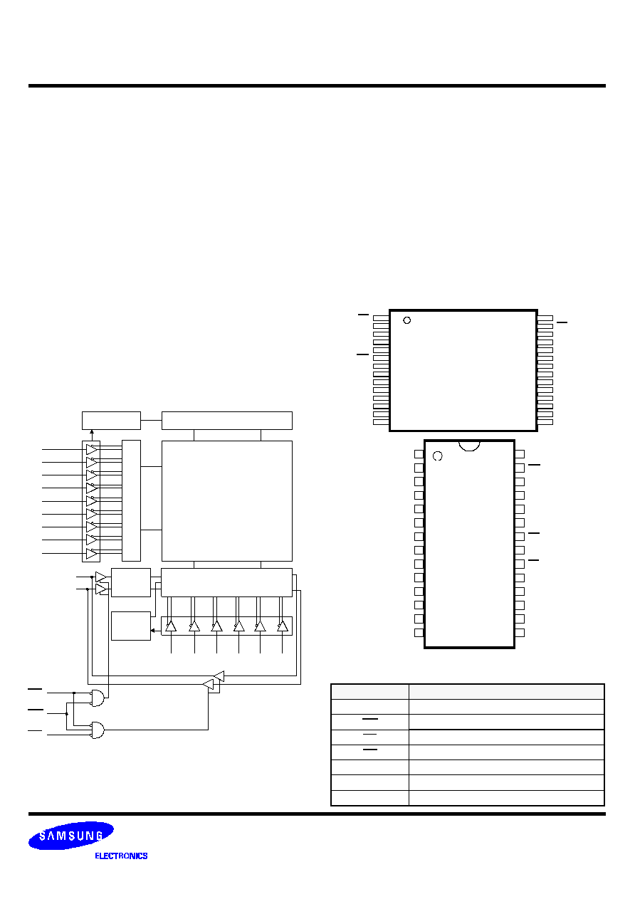
32K x 8 Bit High-Speed CMOS Static RAM
The KM68257C is a 262,144-bit high-speed Static Random
Access Memory organized as 32,768 words by 8 bits. The
KM68257C uses 8 common input and output lines and has an
output enable pin which operates faster than address access
time at read cycle. The device is fabricated using SAMSUNG's
advanced CMOS process and designed for high-speed circuit
technology. It is particularly well suited for use in high-density
high-speed system applications. The KM68257C is packaged in
a 300 mil 28-pin plastic DIP, SOJ or TSOP1 forward.
GENERAL DESCRIPTION
FEATURES
°Ð
Fast Access Time 12, 15, 20
ß¿
(Max.)
°Ð
Low Power Dissipation
Standby (TTL) : 40
ßÃ
(Max.)
(CMOS) : 2
ßÃ
(Max.)
0.1
ßÃ
(Max.)- L-ver. only
Operating KM68257C/CL - 12 : 165
ßÃ
(Max.)
KM68257C/CL - 15 : 150
ßÃ
(Max.)
KM68257C/CL - 20 : 140
ßÃ
(Max.)
°Ð
Single 5.0V
±
10% Power Supply
°Ð
TTL Compatible Inputs and Outputs
°Ð
I/O Compatible with 3.3V Device
°Ð
Fully Static Operation
- No Clock or Refresh required
°Ð
Three State Outputs
°Ð
Low Data Retention Voltage : 2V(Min.)- L-ver. only
°Ð
Standard Pin Configuration
KM68257C/CLP : 28-DIP-300
KM68257C/CLJ : 28-SOJ-300
KM68257C/CLTG : 28-TSOP1-0813, 4F
Clk Gen.
A
3
I/O
1
~ I/O
8
CS
WE
OE
PIN CONFIGURATION
(Top View)
FUNCTIONAL BLOCK DIAGRAM
A
4
A
5
A
6
A
7
A
8
A
12
A
13
A
14
R
o
w
S
e
l
e
c
t
Data
Cont.
A
0
A
1
A
2
A
9
A
10
A
11
CLK
Gen.
Pre-Charge-Circuit
Memory Array
512 Rows
64x8 Columns
SOJ/DIP
TSOP1
1
2
3
4
5
6
7
8
9
10
11
12
13
14
28
27
26
25
24
23
22
21
20
19
18
17
16
15
OE
A11
A9
A8
A13
WE
Vcc
A14
A12
A7
A6
A5
A4
A3
A10
CS
I/O8
I/O7
I/O6
I/O5
I/O4
Vss
I/O3
I/O2
I/O1
A0
A1
A2
1
2
3
4
5
6
7
8
9
10
11
12
13
14
28
27
26
25
24
23
22
21
20
19
18
17
16
15
A14
A12
A7
A6
A5
A4
A3
A2
A1
A0
I/O1
I/O2
I/O3
Vss
Vcc
WE
A13
A8
A9
A11
OE
A10
CS
I/O8
I/O7
I/O6
I/O5
I/O4
Column Select
I/O Circuit
KM68257C/CL
CMOS SRAM
PRELIMINARY
Rev 3.0
- 3 -
February-1996
ABSOLUTE MAXIMUM RATINGS*
* Stresses greater than those listed under "Absolute Maximum Rating" may cause permanent damage to the device. This is a stress ra ting only and func-
tional operation of the device at these at these or any other conditions above those indicated in the operating sections of thi s specification is not
implied. Exposure to absolute maximum rating conditions for extended periods may affect reliability.
Parameter
Symbol
Rating
Unit
Voltage on Any Pin Relative to V
SS
V
IN
,
V
OUT
-0.5 to 7.0
V
Voltage on V
CC
Supply Relative to V
SS
V
CC
-0.5 to 7.0
V
Power Dissipation
P
D
1.0
W
Storage Temperature
T
STG
-65 to 150
∞
C
Operating Temperature
T
A
0 to 70
∞
C
RECOMMENDED DC OPERATING CONDITIONS
(T
A
=0 to 70
∞
C)
* V
IL
(Min) = -2.0(Pulse Width
10ns) for I
20
ßÃ
** V
IH
(Max) = V
CC+
2.0V(Pulse Width
10ns) for I
20
ßÃ
Parameter
Symbol
Min
Typ
Max
Unit
Supply Voltage
V
CC
4.5
5.0
5.5
V
Ground
V
SS
0
0
0
V
Input Low Voltage
V
IH
2.2
-
V
CC
+0.5**
V
Input Low Voltage
V
IL
-0.5*
-
0.8
V
DC AND OPERATING CHARACTERISTICS
(T
A
=0 to 70
∞
C,V
CC
=5.0V
±
10% unless otherwise specified)
* V
CC
=5.0V
±
5% Temp.=25
∞
C
Parameter
Symbol
Test Conditions
Min
Max
Unit
Input Leakage Current
I
LI
V
IN
= V
SS
to
V
CC
-2
2
µ
A
Output Leakage Current
I
LO
CS=V
IH
or OE=V
IH
or WE=V
IL
V
OUT
= V
SS
to
V
CC
-2
2
µ
A
Operating Current
I
CC
Min. Cycle, 100% Duty
CS=V
IL,
V
IN
= V
IH
or
V
IL,
I
OUT
=0mA
12ns
-
165
ßÃ
15ns
-
150
20ns
-
140
Standby Current
I
SB
Min. Cycle, CS=V
IH
-
40
ßÃ
I
SB
1
f=0MHz, CS
V
CC
-0.2V,
V
IN
V
CC
-0.2V or
V
IN
0.2V
Normal
-
2
ßÃ
L-ver
-
0.1
Output Low Voltage Level
V
OL
I
OL
=8mA
-
0.4
V
Output High Voltage Level
V
OH
I
OH
=-4mA
2.4
-
V
V
OH1*
I
OH1
=0.1mA
-
3.95
V
CAPACITANCE*
(T
A
=25
∞
C, f=1.0MHz)
* NOTE : Capacitance is sampled and not 100% tested.
Item
Symbol
Test Conditions
MIN
Max
Unit
Input/Output Capacitance
C
I/O
V
I/O
=0V
-
8
pF
Input Capacitance
C
IN
V
IN
=0V
-
7
pF
KM68257C/CL
CMOS SRAM
PRELIMINARY
Rev 3.0
- 4 -
February-1996
TEST CONDITIONS
Parameter
Value
Input Pulse Levels
0V to 3V
Input Rise and Fall Times
3
ß¿
Input and Output timing Reference Levels
1.5V
Output Loads
See below
AC CHARACTERISTICS
(T
A
=0
to 70
∞
C, V
CC
=5.0V
±
10%, unless otherwise noted.)
Output Loads(A)
Output Loads(B)
DOUT
5pF*
480
255
for t
HZ
, t
LZ
, t
WHZ
, t
OW
, t
OLZ
& t
OHZ
+5.0V
READ CYCLE
Parameter
Symbol
KM68257C/CL-12
KM68257C/CL-15
KM68257C/CL-20
Unit
Min
Max
Min
Max
Min
Max
Read Cycle Time
t
RC
12
-
15
-
20
-
ß¿
Address Access Time
t
AA
-
12
-
15
-
20
ß¿
Chip Select to Output
t
CO
-
12
-
15
-
20
ß¿
Output Enable to Valid Output
t
OE
-
6
-
7
-
9
ß¿
Chip Enable to Low-Z Output Access
t
LZ
3
-
3
-
3
-
ß¿
Output Enable to Low-Z Output
t
OLZ
0
-
0
-
0
-
ß¿
Chip Disable to High-Z Output
t
HZ
0
6
0
7
0
10
ß¿
Output Disable to High-Z Output
t
OHZ
0
6
0
7
0
10
ß¿
Output Hold from Address Change
t
OH
3
-
3
-
3
-
ß¿
Chip Selection to Power Up Time
t
PU
0
-
0
-
0
-
ß¿
Chip Selection to Power DownTime
t
PD
-
12
-
15
-
20
ß¿
DOUT
30pF*
480
255
+5V
* Including Scope and Jig Capacitance
KM68257C/CL
CMOS SRAM
PRELIMINARY
Rev 3.0
- 5 -
February-1996
WRITE CYCLE
Parameter
Symbol
KM68257C/CL-12
KM68257C/CL-15
KM68257C/CL-20
Unit
Min
Max
Min
Max
Min
Max
Write Cycle Time
t
WC
12
-
15
-
20
-
ß¿
Chip Select to End of Write
t
CW
9
-
11
-
13
-
ß¿
Address Setup Time
t
AS
0
-
0
-
0
-
ß¿
Address Valid to End of Write
t
AW
9
-
12
-
13
-
ß¿
Write Pulse Width(OE High)
t
WP
9
-
12
-
13
-
ß¿
Write Pulse Width(OE Low)
t
WP1
12
-
15
-
20
-
ß¿
Write Recovery Time
t
WR
0
-
0
-
0
-
ß¿
Write to Output High-Z
t
WHZ
0
6
0
8
0
8
ß¿
Data to Write Time Overlap
t
DW
7
-
8
-
10
-
ß¿
Data Hold from Write Time
t
DH
0
-
0
-
0
-
ß¿
End Write to Output Low-Z
t
OW
0
-
0
-
0
-
ß¿
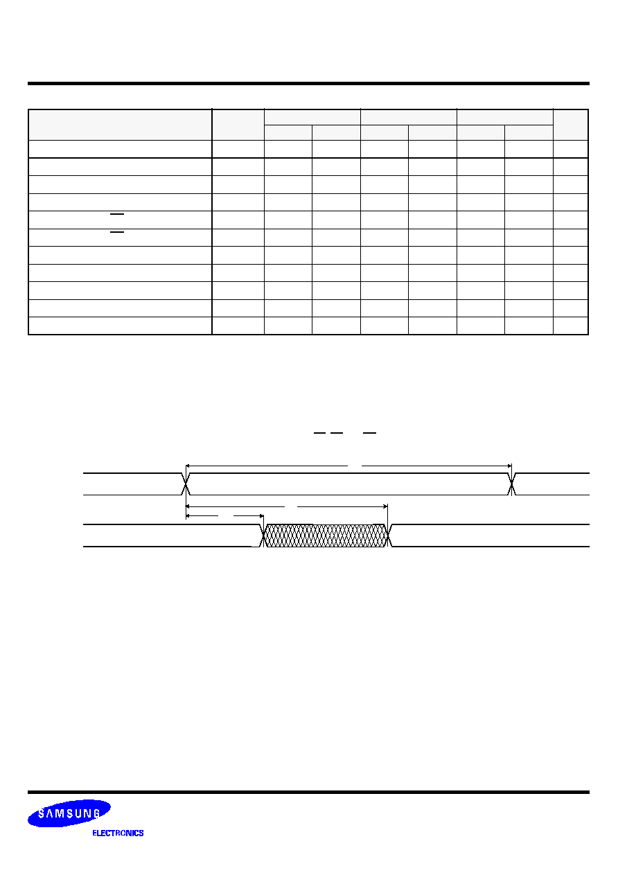
TIMING DIAGRAMS
TIMING WAVE FORM OF READ CYCLE(1)
(Address Controlled, CS=OE=V
IL
, WE=V
IH
)
ADD
Data Out
Previous Data Valid
Data Valid
t
RC
t
AA
t
OH
KM68257C/CL
CMOS SRAM
PRELIMINARY
Rev 3.0
- 6 -
February-1996
TIMING WAVE FORM OF READ CYCLE(2)
(WE=VIH)
CS
OE
Data Out
ADD
NOTES(READ CYCLE)
1. WE is high for read cycle.
2. All read cycle timing is referenced from the last valid address to the first transition address.
3. t
HZ
and t
OHZ
are defined as the time at which the outputs achieve the open circuit condition and are not referenced to V
OH
or V
OL
Levels.
4. At any given temperature and voltage condition, t
HZ
(Max.) is less than t
LZ
(Min.) both for a given device and from device to device.
5. Transition is measured
±
200
ß∆
from steady state voltage with Load(B). This parameter is sampled and not 100% tested.
6. Device is continuously selected with CS=V
IL.
7. Address valid prior to coincident with CS transition low.
8. For common I/O applications, minimization or elimination of bus contention conditions is necessary during read and write cycl e.
TIMING WAVE FORM OF WRITE CYCLE(1)
(OE=Clock)
OE
CS
Data In
WE
High-Z
ADD
Data Out
Data Valid
High-Z(8)
50%
50%
Vcc
Current
Data Valid
Icc
I
SB
t
RC
t
AA
t
CO
t
HZ(3,4,5)
t
OHZ
t
OH
t
PD
t
LZ(4,5)
t
OLZ
t
OE
t
PU
t
WC
t
AW
t
CW(3)
t
WP(2)
t
AS(4)
t
DW
t
DH
t
OHZ(6)
t
WR(5)
KM68257C/CL
CMOS SRAM
PRELIMINARY
Rev 3.0
- 7 -
February-1996
TIMING WAVE FORM OF WRITE CYCLE(3)
(CS=Controlled)
CS
Data In
WE
High-Z
ADD
Data Out
Data Valid
High-Z
(8)
High-Z
TIMING WAVE FORM OF WRITE CYCLE(2)
(OE=Low Fixed)
CS
Data In
WE
High-Z
ADD
Data Out
Data Valid
High-Z
(8)
(10)
(9)
High-Z
t
WC
t
AW
t
CW(3)
t
WP1(2)
t
AS(4)
t
DW
t
DH
t
OW
t
WHZ(6)
t
OH
t
WC
t
AW
t
CW(3)
t
WP(2)
t
AS(4)
t
LZ
t
DW
t
WHZ(6)
t
DH
t
WR(5)
t
WR(5)
KM68257C/CL
CMOS SRAM
PRELIMINARY
Rev 3.0
- 8 -
February-1996
NOTES(WRITE CYCLE)
1. All write cycle timing is referenced from the last valid address to the first transition address.
2. A write occurs during the overlap of a low CS and WE. A write begins at the latest transition CS going low and WE going low ; A write ends at the ear-
liest transition CS going high or WE going high. t
WP
is measured from the beginning of write to the end of write.
3. t
CW
is measured from the later of CS going low to end of write.
4. t
AS
is measured from the address valid to the beginning of write.
5. t
WR
is measured from the end of write to the address change. t
WR
applied in case a write ends as CS or WE going high.
6. If OE, CS and WE are in the Read Mode during this period, the I/O pins are in the output low-Z state. Inputs of opposite phase of the output mus t not
be applied because bus contention can occur.
7. For common I/O applications, minimization or elimination of bus contention conditions is necessary during read and write cycl e.
8. If CS goes low simultaneously with WE going or after WE going low, the outputs remain high impedance state.
9. Dout is the read data of the new address.
10. When CS is low : I/O pins are in the output state. The input signals in the opposite phase leading to the output should not be applied.
FUNCTIONAL DESCRIPTION
* NOTE : X means Don't Care.
CS
WE
OE
Mode
I/O Pin
Supply Current
H
X
X*
Not Select
High-Z
I
SB
, I
SB1
L
H
H
Output Disable
High-Z
I
CC
L
H
L
Read
D
OUT
I
CC
L
L
X
Write
D
IN
I
CC
DATA RETENTION CHARACTERISTICS*
(T
A
= 0 to 70
∞
C)
* L-Ver only.
Parameter
Symbol
Test Condition
Min.
Typ.
Max.
Unit
V
CC
for Data Retention
V
DR
CS
V
CC
- 0.2V
2.0
-
5.5
V
Data Retention Current
I
DR
V
CC
= 3.0V, CS
V
CC
- 0.2V
V
IN
V
CC
- 0.2V or V
IN
0.2V
-
-
0.07
ßÃ
Data Retention Set-Up Time
t
SDR
See Data Retention
Wave form(below)
0
-
-
ns
Recovery Time
t
RDR
5
-
-
ms
DATA RETENTION WAVE FORM
(CS Controlled)
V
CC
4.5V
2.2V
V
DR
CS
GND
Data Retention Mode
CS
V
CC
- 0.2V
t
SDR
t
RDR
KM68257C/CL
CMOS SRAM
PRELIMINARY
Rev 3.0
- 9 -
February-1996
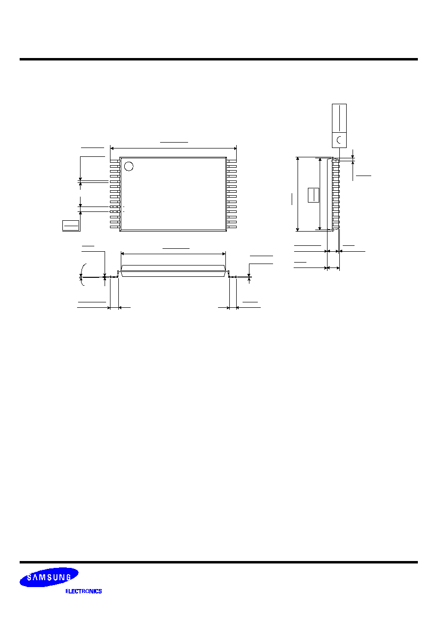
PACKAGE DIMENSIONS
Units : Inches (millimeters)
0~15
°…
0.65
MAX
#1
28-DIP-300
#28
7.01
±
0.20
0.276
±
0.008
34.29
±
0.20
1.350
±
0.008
( )
0.025
3.81
±
0.20
0.150
±
0.008
5.08
0.200
MIN
0.020
0.51
7
.
6
2
0
.
3
0
0
+0.10
MAX
34.69
1.366
0.25
-0.05
+0.004
0.010
-0.002
#14
#15
2.54
0.100
+0.30
3.18
-0.25
+0.012
0.125
-0.010
1.27
±
0.10
0.050
±
0.004
0.46
±
0.10
0.018
±
0.004
#1
28-SOJ-300
#28
8.51
±
0.12
0.335
±
0.005
18.41
±
0.12
0.725
±
0.005
7
.
6
2
0
.
3
0
0
+0.10
MAX
18.82
0.741
0.20
-0.05
+0.004
0.008
-0.002
6.86
±
0.25
0.270
±
0.010
MAX
0.148
3.76
MIN
0.69
0.027
1.30
( )
0.051
1.30
( )
0.051
#14
#15
0.95
( )
0.0375
+0.10
0.43
-0.05
+0.004
0.017
-0.002
+0.10
0.71
-0.05
+0.004
0.028
-0.002
1.27
0.050
0.004
0.10 MAX
KM68257C/CL
CMOS SRAM
PRELIMINARY
Rev 3.0
- 10
February-1996
PACKAGE DIMENSIONS
28-TSOP1-0813.4F
PACKAGE DIMENSIONS
Units : Inches (millimeters)
#28
1.00
±
0.10
0.039
±
0.004
M
A
X
8
.
4
0
0
.
3
3
1
0
.
0
0
4
M
A
X
1
.
1
0
M
A
X
#1
0.50
( )
0.020
11.80
±
0.10
0.465
±
0.004
0.45 ~0.75
0.018 ~0.030
13.40
±
0.20
0.528
±
0.008
#15
#14
+0.10
0.15
-0.05
+0.004
0.006
-0.002
0~8
°…
+0.10
0.20
-0.05
+0.004
0.008
-0.002
0.55
0.0217
0.425
( )
0.017
MIN
0.05
0.002
MAX
1.20
0.047
8
.
0
0
0
.
3
1
5
TYP
0.25
0.010