736v789.PDF

KM736V789
128Kx36 Synchronous SRAM
- 1 -
Rev 3.0
November 1999
Document Title
128Kx36-Bit Synchronous Pipelined Burst SRAM
The attached data sheets are prepared and approved by SAMSUNG Electronics. SAMSUNG Electronics CO., LTD. reserve the right to change the
specifications. SAMSUNG Electronics will evaluate and reply to your requests and questions on the parameters of this device. If you have any ques-
tions, please contact the SAMSUNG branch office near your office, call or contact Headquarters.
Revision History
Rev. No.
0.0
0.1
0.2
0.3
0.4
0.5
0.6
0.7
1.0
2.0
3.0
Remark
Preliminary
Preliminary
Preliminary
Preliminary
Preliminary
Preliminary
Preliminary
Preliminary
Final
Final
Final
History
Initial draft
Change 7.5 bin to 7.2
Change speed symbol 6.0/6.7/7.2/8.5 to 60/67/72/85
Change DC characteristics V
DD
condition from V
DD
=3.3V+10%/-5% Change
Input/output leackage currant for
±
1
µ
A to
±
2
µ
A
Modify Read timing & Power down cycle timing.
Change I
SB2
value from 30mA to 20mA.
Remove DC characteristics I
SB1
- L ver.& I
SB2
- L ver .
Remove Low power version.
Add 119BGA(7x17 Ball Grid Array Package)
Change Undershoot spec
from -3.0V(pulse width
20ns) to -2.0V(pulse width
t
CYC
/2)
Add Overshoot spec 4.6V((pulse width
t
CYC
/2)
Change V
IH
max from 5.5V to V
DD
+0.5V
Change I
SB2
value from 20mA to 30mA.
Change V
DD
condition from V
DD
=3.3V+10%/-5% to V
DD
=3.3V+0.3V/-0.165V.
Modify DC characteristics( Input Leakage Current test Conditions)
form V
DD
=V
SS to
V
DD
to Max.
Final spec Release
Add V
DDQ
Supply voltage( 2.5V )
Remove 119BGA(7x17 Ball Grid Array Package) .
Draft Date
May . 15. 1997
January . 13 . 1998
February. 02. 1998
February. 12. 1998
March. 11 . 1998
April. 14. 1998
May.13. 1998
May.14.1998
May. 15. 1998
Dec. 02. 1998
Nov. 26. 1999
KM736V789
128Kx36 Synchronous SRAM
- 2 -
Rev 3.0
November 1999
WEc
WEd
128Kx36-Bit Synchronous Pipelined Burst SRAM
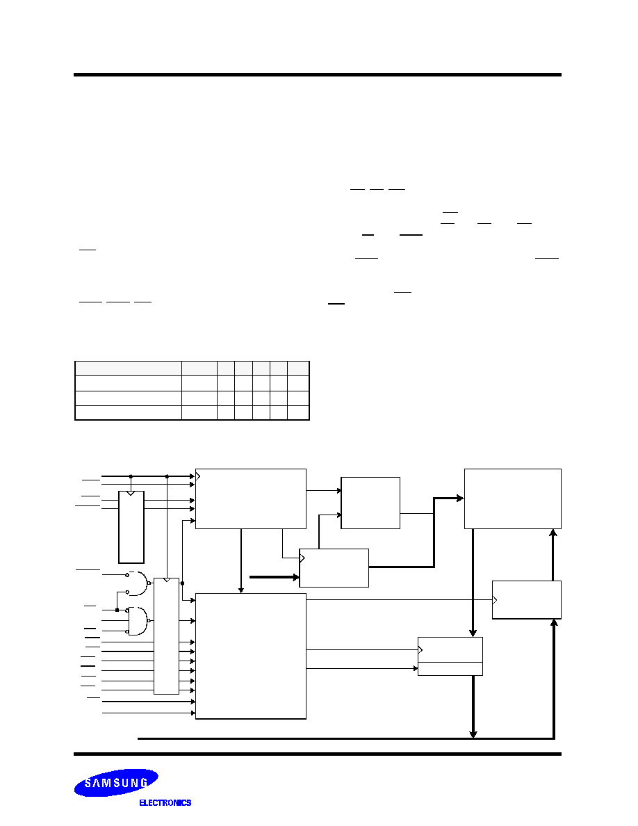
The KM736V789 is a 4,718,592-bit Synchronous Static Ran-
dom Access Memory designed for high performance second
level cache of Pentium and Power PC based System.
It is organized as 128K words of 36bits and integrates address
and control registers, a 2-bit burst address counter and added
some new functions for high performance cache RAM applica-
tions; GW, BW, LBO, ZZ. Write cycles are internally self-timed
and synchronous.
Full bus-width write is done by GW, and each byte write is per-
formed by the combination of WEx and BW when GW is high.
And with CS
1
high, ADSP is blocked to control signals.
Burst cycle can be initiated with either the address status pro-
cessor(ADSP) or address status cache controller(ADSC)
inputs. Subsequent burst addresses are generated internally in
the system
s burst sequence and are controlled by the burst
address advance(ADV) input.
LBO pin is DC operated and determines burst sequence(linear
or interleaved).
ZZ pin controls Power Down State and reduces Stand-by cur-
rent regardless of CLK.
The KM736V789 is fabricated using SAMSUNG
s high perfor-
mance CMOS technology and is available in a 100pin TQFP
package. Multiple power and ground pins are utilized to mini-
mize ground bounce.
GENERAL DESCRIPTION
FEATURES
LOGIC BLOCK DIAGRAM
·
Synchronous Operation.
·
2 Stage Pipelined operation with 4 Burst.
·
On-Chip Address Counter.
·
Self-Timed Write Cycle.
·
On-Chip Address and Control Registers.
·
V
DD
= 3.3V+0.3V/-0.165V Power Supply.
· V
DDQ
Supply Voltage 3.3V+0.3V/-0.165V for 3.3V I/O
or 2.5V+0.4V/-0.125V for 2.5V I/O.
·
5V Tolerant Inputs Except I/O Pins.
·
Byte Writable Function.
·
Global Write Enable Controls a full bus-width write.
·
Power Down State via ZZ Signal.
·
LBO Pin allows a choice of either a interleaved burst or a lin-
ear burst.
·
Three Chip Enables for simple depth expansion with No Data
Contention ; 2cycle Enable, 1cycle Disable.
·
Asynchronous Output Enable Control.
·
ADSP, ADSC, ADV Burst Control Pins.
·
TTL-Level Three-State Output.
·
100-TQFP-1420A Package .
CLK
LBO
ADV
ADSC
ADSP
CS
1
CS
2
CS
2
GW
BW
WEa
WEb
OE
ZZ
DQa
0
~ DQd
7
BURST CONTROL
LOGIC
BURST
128Kx36
ADDRESS
CONTROL
OUTPUT
DATA-IN
ADDRESS
COUNTER
MEMORY
ARRAY
REGISTER
REGISTER
BUFFER
LOGIC
C
O
N
T
R
O
L
R
E
G
I
S
T
E
R
C
O
N
T
R
O
L
R
E
G
I
S
T
E
R
A
0
~A
1
A
0
~A
1
A
2
~A
16
A
0
~A
16
REGISTER
FAST ACCESS TIMES
PARAMETER
Symbol 60
67
72
85 Unit
Cycle Time
t
CYC
6.0 6.7 7.2 8.5
ns
Clock Access Time
t
CD
3.5 3.8 4.0 4.0
ns
Output Enable Access Time
t
OE
3.5 3.8 4.0 4.0
ns
DQPa ~ DQPd
KM736V789
128Kx36 Synchronous SRAM
- 3 -
Rev 3.0
November 1999
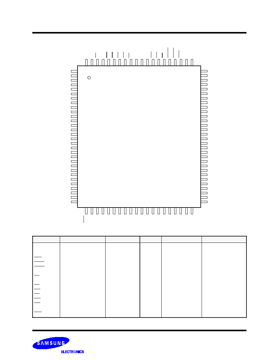
PIN CONFIGURATION
(TOP VIEW)
1
2
3
4
5
6
7
8
9
10
11
12
13
14
15
16
17
18
19
20
21
22
23
24
25
26
27
28
29
30
100 Pin
(20mm x 14mm)
DQPc
DQc
0
DQc
1
V
DDQ
V
SSQ
DQc
2
DQc
3
DQc
4
DQc
5
V
SSQ
V
DDQ
DQc
6
DQc
7
N.C.
V
DD
N.C.
V
SS
DQd
0
DQd
1
V
DDQ
V
SSQ
DQd
2
DQd
3
DQd
4
DQd
5
V
SSQ
V
DDQ
DQd
6
DQd
7
DQPd
80
79
78
77
76
75
74
73
72
71
70
69
68
67
66
65
64
63
62
61
60
59
58
57
56
55
54
53
52
51
DQPb
DQb
7
DQb
6
V
DDQ
V
SSQ
DQb
5
DQb
4
DQb
3
DQb
2
V
SSQ
V
DDQ
DQb
1
DQb
0
V
SS
N.C.
V
DD
ZZ
DQa
7
DQa
6
V
DDQ
V
SSQ
DQa
5
DQa
4
DQa
3
DQa
2
V
SSQ
V
DDQ
DQa
1
DQa
0
DQPa
1
0
0
9
9
9
8
9
7
9
6
9
5
9
4
9
3
9
2
9
1
9
0
8
9
8
8
8
7
8
6
8
5
8
4
8
3
8
2
A
6
A
7
C
S
1
C
S
2
W
E
d
W
E
c
W
E
b
W
E
a
C
S
2
V
D
D
V
S
S
C
L
K
G
W
B
W
O
E
A
D
S
C
A
D
S
P
A
D
V
A
8
8
1
A
9
5
0
4
9
4
8
4
7
4
6
4
5
4
4
4
3
4
2
4
1
4
0
3
9
3
8
3
7
3
6
3
5
3
4
3
3
3
2
A
1
6
A
1
5
A
1
4
A
1
3
A
1
2
A
1
1
A
1
0
N
.
C
.
N
.
C
.
V
D
D
V
S
S
N
.
C
.
N
.
C
.
A
0
A
1
A
2
A
3
A
4
A
5
3
1
L
B
O
PIN NAME
SYMBOL
PIN NAME
TQFP PIN NO.
SYMBOL
PIN NAME
TQFP PIN NO.
A
0
- A
16
ADV
ADSP
ADSC
CLK
CS
1
CS
2
CS
2
WEx(x=a,b,c,d)
OE
GW
BW
ZZ
LBO
Address Inputs
Burst Address Advance
Address Status Processor
Address Status Controller
Clock
Chip Select
Chip Select
Chip Select
Byte Write Inputs
Output Enable
Global Write Enable
Byte Write Enable
Power Down Input
Burst Mode Control
32,33,34,35,36,37,
44,45,46,47,48,49,
50,81,82,99,100
83
84
85
89
98
97
92
93,94,95,96
86
88
87
64
31
V
DD
V
SS
N.C.
DQa
0
~a
7
DQb
0
~b
7
DQc
0
~c
7
DQd
0
~d
7
DQPa~P
d
V
DDQ
V
SSQ
Power Supply(+3.3V)
Ground
No Connect
Data Inputs/Outputs
Output Power Supply
(2.5V or 3.3V)
Output Ground
15,41,65,91
17,40,67,90
14,16,38,39,42,43,66
52,53,56,57,58,59,62,63
68,69,72,73,74,75,78,79
2,3,6,7,8,9,12,13
18,19,22,23,24,25,28,29
51,80,1,30
4,11,20,27,54,61,70,77
5,10,21,26,55,60,71,76
TQFP
KM736V789
128Kx36 Synchronous SRAM
- 4 -
Rev 3.0
November 1999
FUNCTION DESCRIPTION
The KM736V789 is a synchronous SRAM designed to support the burst address accessing sequence of the P6 and Power PC based
microprocessor. All inputs (with the exception of OE, LBO and ZZ) are sampled on rising clock edges. The start and duration of the
burst access is controlled by ADSC, ADSP and ADV and chip select pins.
The accesses are enabled with the chip select signals and output enabled signals. Wait states are inserted into the access with
ADV.
When ZZ is pulled high, the SRAM will enter a Power Down State. At this time, internal state of the SRAM is preserved. When ZZ
returns to low, the SRAM normally operates after 2cycles of wake up time. ZZ pin is pulled down internally.
Read cycles are initiated with ADSP(regardless of WEx and ADSC)using the new external address clocked into the on-chip address
register whenever ADSP is sampled low, the chip selects are sampled active, and the output buffer is enabled with OE. In read oper-
ation the data of cell array accessed by the current address, registered in the Data-out registers by the positive edge of CLK, are car-
ried to the Data-out buffer by the next positive edge of CLK. The data, registered in the Data-out buffer, are projected to the output
pins. ADV is ignored on the clock edge that samples ADSP asserted, but is sampled on the subsequent clock edges. The address
increases internally for the next access of the burst when WEx are sampled High and ADV is sampled low. And ADSP is blocked to
control signals by disabling CS
1
.
All byte write is done by GW(regaedless of BW and WEx.), and each byte write is performed by the combination of BW and WEx
when GW is high.
Write cycles are performed by disabling the output buffers with OE and asserting WEx. WEx are ignored on the clock edge that sam-
ples ADSP low, but are sampled on the subsequent clock edges. The output buffers are disabled when WEx are sampled
Low(regaedless of OE). Data is clocked into the data input register when WEx sampled Low. The address increases internally to the
next address of burst, if both WEx and ADV are sampled Low. Individual byte write cycles are performed by any one or more byte
write enable signals(WEa, WEb, WEc or WEd) sampled low. The WEa control DQa
0
~ DQa
7
and DQPa, WEb controls DQb
0
~ DQb
7
and DQPb,
WEc controls DQc
0
~ DQc
7
and DQPc,
and WEd control DQd
0
~ DQd
7
and DQPd. Read or write cycle may also be initi-
ated with ADSC, instead of ADSP. The differences between cycles initiated with ADSC and ADSP as are follows;
ADSP must be sampled high when ADSC is sampled low to initiate a cycle with ADSC.
WEx are sampled on the same clock edge that sampled ADSC low(and ADSP high).
Addresses are generated for the burst access as shown below, The starting point of the burst sequence is provided by the external
address. The burst address counter wraps around to its initial state upon completion. The burst sequence is determined by the state
of the LBO pin. When this pin is Low, linear burst sequence is selected. When this pin is High, Interleaved burst sequence is
selected.
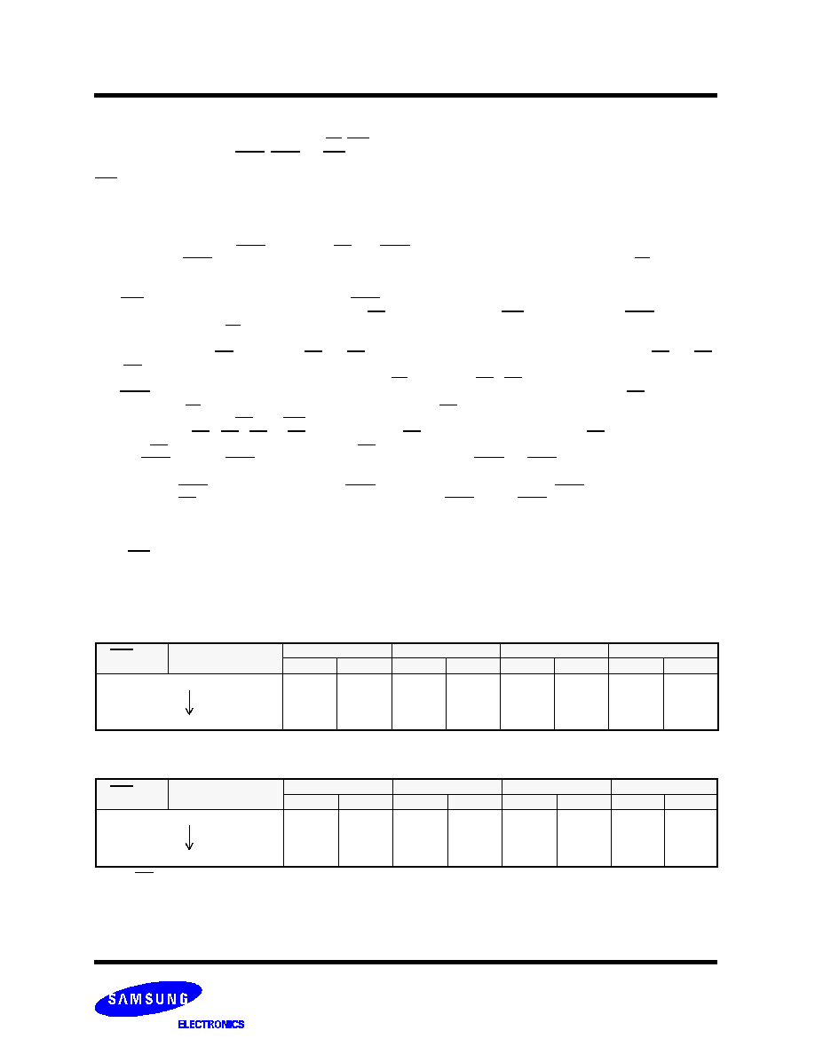
BURST SEQUENCE TABLE
(Interleaved Burst)
LBO PIN
HIGH
Case 1
Case 2
Case 3
Case 4
A
1
A
0
A
1
A
0
A
1
A
0
A
1
A
0
First Address
Fourth Address
0
0
1
1
0
1
0
1
0
0
1
1
1
0
1
0
1
1
0
0
0
1
0
1
1
1
0
0
1
0
1
0
BQ TABLE
(Linear Burst)
Note : 1. LBO pin must be tied to High or Low, and Floating State must not be allowed
.
LBO PIN
LOW
Case 1
Case 2
Case 3
Case 4
A
1
A
0
A
1
A
0
A
1
A
0
A
1
A
0
First Address
Fourth Address
0
0
1
1
0
1
0
1
0
1
1
0
1
0
1
0
1
1
0
0
0
1
0
1
1
0
0
1
1
0
1
0
KM736V789
128Kx36 Synchronous SRAM
- 5 -
Rev 3.0
November 1999
SYNCHRONOUS TRUTH TABLE
Notes : 1. X means "Don
t Care". 2. The rising edge of clock is symbolized by
.
3. WRITE = L means Write operation in WRITE TRUTH TABLE.
WRITE = H means Read operation in WRITE TRUTH TABLE.
4. Operation finally depends on status of asynchronous input pins(ZZ and OE).
CS
1
CS
2
CS
2
ADSP ADSC
ADV
WRITE
CLK
ADDRESS ACCESSED
OPERATION
H
X
X
X
L
X
X
N/A
Not Selected
L
L
X
L
X
X
X
N/A
Not Selected
L
X
H
L
X
X
X
N/A
Not Selected
L
L
X
X
L
X
X
N/A
Not Selected
L
X
H
X
L
X
X
N/A
Not Selected
L
H
L
L
X
X
X
External Address
Begin Burst Read Cycle
L
H
L
H
L
X
L
External Address
Begin Burst Write Cycle
L
H
L
H
L
X
H
External Address
Begin Burst Read Cycle
X
X
X
H
H
L
H
Next Address
Continue Burst Read Cycle
H
X
X
X
H
L
H
Next Address
Continue Burst Read Cycle
X
X
X
H
H
L
L
Next Address
Continue Burst Write Cycle
H
X
X
X
H
L
L
Next Address
Continue Burst Write Cycle
X
X
X
H
H
H
H
Current Address
Suspend Burst Read Cycle
H
X
X
X
H
H
H
Current Address
Suspend Burst Read Cycle
X
X
X
H
H
H
L
Current Address
Suspend Burst Write Cycle
H
X
X
X
H
H
L
Current Address
Suspend Burst Write Cycle
WRITE TRUTH TABLE
Notes : 1. X means "Don
t Care".
2. All inputs in this table must meet setup and hold time around the rising edge of CLK(
).
GW
BW
WEa
WEb
WEc
WEd
OPERATION
H
H
X
X
X
X
READ
H
L
H
H
H
H
READ
H
L
L
H
H
H
WRITE BYTE a
H
L
H
L
H
H
WRITE BYTE b
H
L
H
H
L
L
WRITE BYTE c and d
H
L
L
L
L
L
WRITE ALL BYTEs
L
X
X
X
X
X
WRITE ALL BYTEs
ASYNCHRONOUS TRUTH TABLE
(See Notes 1 and 2)
:
OPERATION
ZZ
OE
I/O STATUS
Sleep Mode
H
X
High-Z
Read
L
L
DQ
L
H
High-Z
Write
L
X
Din, High-Z
Deselected
L
X
High-Z
TRUTH TABLES
Notes
1. X means "Don
t Care".
2. ZZ pin is pulled down internally
3. For write cycles that following read cycles, the output buffers must be
disabled with OE, otherwise data bus contention will occur.
4. Sleep Mode means power down state of which stand-by current does
not depend on cycle time.
5. Deselected means power down state of which stand-by current
depends on cycle time.