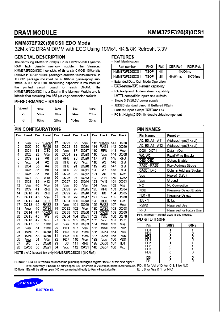
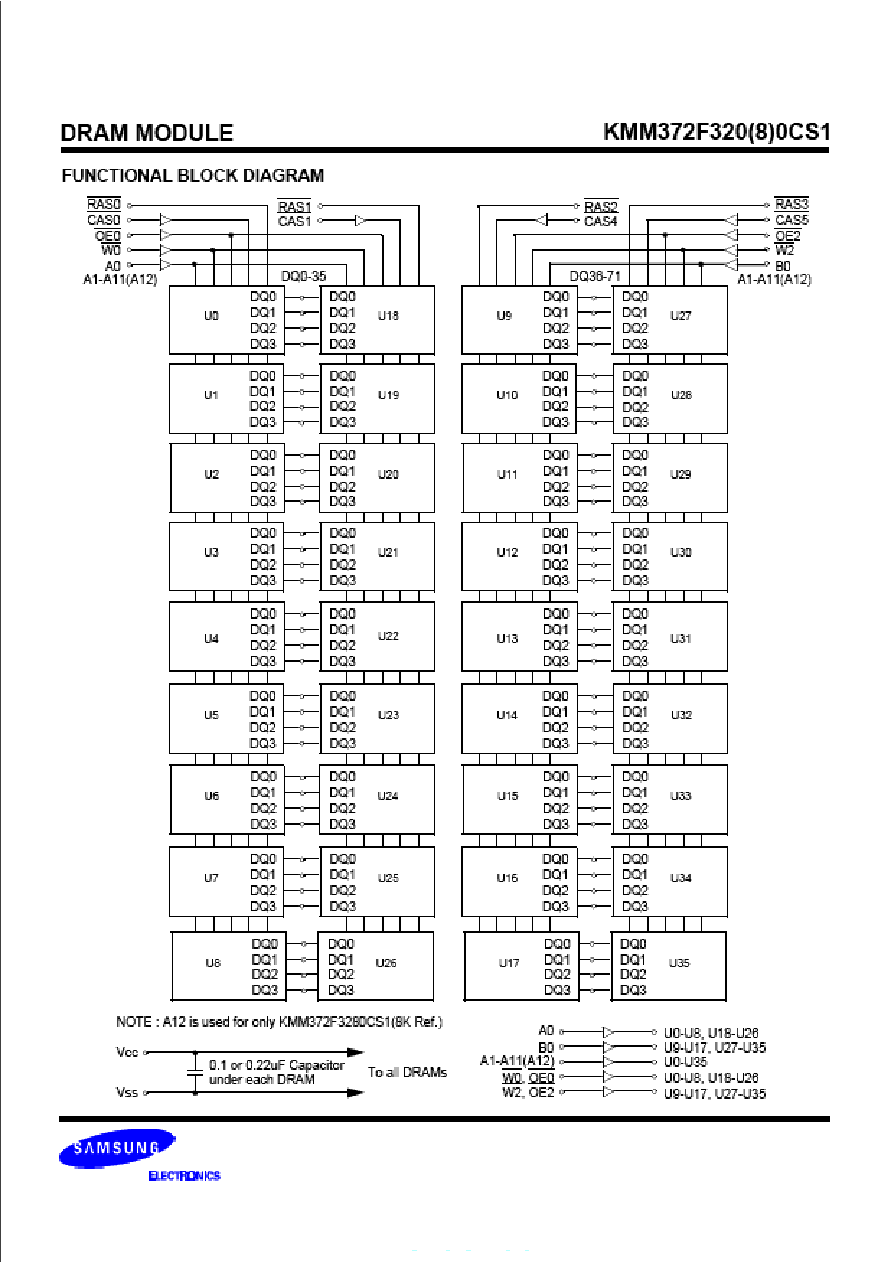
DRAM MODULE
KMM372F320(8)0CS1
I
CC1
, I
CC3
, I
CC4
and I
CC6
are dependent on output loading and cycle rates. Specified values are obtained with the output open.
I
CC
is specified as an average current. In I
CC1
and I
CC3
, address can be changed maximum once while RAS=V
IL
. In I
CC4
,
address can be changed maximum once within one EDO mode cycle time,
t
HPC
.
* NOTE :
DC AND OPERATING CHARACTERISTICS
(Recommended operating conditions unless otherwise noted)
I
CC1
*
I
CC2
I
CC3
*
I
CC4
*
I
CC5
I
CC6
*
I(
IL)
I(
OL)
V
OH
V
OL
Symbol
Speed
KMM372F3200CS1
KMM372F3280CS1
Unit
Min
Max
Min
Max
I
CC1
-5
-6
-
-
1998
1818
-
-
1458
1278
mA
mA
I
CC2
Don
t care
-
100
-
100
mA
I
CC3
-5
-6
-
-
1998
1818
-
-
1458
1278
mA
mA
I
CC4
-5
-6
-
-
1638
1458
-
-
1638
1458
mA
mA
I
CC5
Don
t care
-
30
-
30
mA
I
CC6
-5
-6
-
-
1998
1818
-
-
1998
1818
mA
mA
I
I(L)
I
O(L)
Don
t care
-10
-10
10
10
-10
-10
10
10
uA
uA
V
OH
V
OL
Don
t care
2.4
-
-
0.4
2.4
-
-
0.4
V
V
: Operating Current * (RAS, CAS, Address cycling @
t
RC
=min)
: Standby Current (RAS=CAS=W=V
IH
)
: RAS Only Refresh Current * (CAS=V
IH
, RAS cycling @
t
RC
=min)
: Extended Data Out Mode Current * (RAS=V
IL
, CAS cycling :
t
HPC
=min)
: Standby Current (RAS=CAS=W=Vcc-0.2V)
: CAS-Before-RAS Refresh Current * (RAS and CAS cycling @
t
RC
=min)
: Input Leakage Current (Any input 0
V
IN
Vcc+0.3V, all other pins not under test=0 V)
: Output Leakage Current(Data Out is disabled, 0V
V
OUT
Vcc)
: Output High Voltage Level (I
OH
= -2mA)
: Output Low Voltage Level (I
OL
= 2mA)
RECOMMENDED OPERATING CONDITIONS
(Voltage referenced to V
SS
, T
A
= 0 to 70
∞
C)
*1 : V
CC
+1.3V at pulse width
15ns, which is measured at V
CC
.
*2 : -1.3V at pulse width
15ns, which is measured at V
SS
.
Item
Symbol
Min
Typ
Max
Unit
Supply Voltage
Ground
Input High Voltage
Input Low Voltage
V
CC
V
SS
V
IH
V
IL
3.0
0
2.0
-0.3
*2
3.3
0
-
-
3.6
0
V
CC
+0.3
*1
0.8
V
V
V
V
ABSOLUTE MAXIMUM RATINGS *
* Permanent device damage may occur if ABSOLUTE MAXIMUM RATINGS are exceeded. Functional operation should be restricted to
the conditions as detailed in the operational sections of this data sheet. Exposure to absolute maximum rating conditions for intended
periods may affect device reliability.
Item
Symbol
Rating
Unit
Voltage on any pin relative V
SS
Voltage on V
CC
supply relative to V
SS
Storage Temperature
Power Dissipation
Short Circuit Output Current
V
IN
, V
OUT
V
CC
T
stg
P
D
I
OS
-0.5 to +4.6
-0.5 to +4.6
-55 to +125
36
50
V
V
∞
C
W
mA
DRAM MODULE
KMM372F320(8)0CS1
CAPACITANCE
(T
A
= 25
∞
C, f = 1MHz)
Item
Symbol
Min
Max
Unit
Input capacitance[A0, B0, A1 - A12]
Input capacitance[W0, W2, OE0, OE2]
Input capacitance[RAS0 - RAS3]
Input capacitance[CAS0, 1,4,5]
Input/Output capacitance[DQ0 - 71]
C
IN1
C
IN2
C
IN3
C
IN4
C
DQ
-
-
-
-
-
20
20
73
20
24
pF
pF
pF
pF
pF
Test condition : V
ih
/V
il
=2.2/0.7V, V
oh
/V
ol
=2.0/0.8V, output loading CL=100pF
Parameter
Symbol
-5
-6
Unit
Note
Min
Max
Min
Max
Random read or write cycle time
t
RC
84
104
ns
Read-modify-write cycle time
t
RWC
128
153
ns
Access time from RAS
t
RAC
50
60
ns
3,4,10
Access time from CAS
t
CAC
18
20
ns
3,4,5,13
Access time from column address
t
AA
30
35
ns
3,10,13
CAS to output in Low-Z
t
CLZ
8
8
ns
3,13
OE to output in Low-Z
t
OLZ
8
8
ns
3,13
Output buffer turn-off delay from CAS
t
CEZ
8
18
8
18
ns
6,11,13
Transition time(rise and fall)
t
T
1
50
1
50
ns
2
RAS precharge time
t
RP
30
40
ns
RAS pulse width
t
RAS
50
10K
60
10K
ns
RAS hold time
t
RSH
13
15
ns
13
CAS hold time
t
CSH
36
38
ns
13
CAS pulse width
t
CAS
8
10K
10
10K
ns
RAS to CAS delay time
t
RCD
15
32
18
40
ns
4,13
RAS to column address delay time
t
RAD
10
20
13
25
ns
10,13
CAS to RAS precharge time
t
CRP
10
10
ns
13
Row address set-up time
t
ASR
5
5
ns
13
Row address hold time
t
RAH
5
8
ns
13
Column address set-up time
t
ASC
0
0
ns
Column address hold time
t
CAH
7
10
ns
Column address to RAS lead time
t
RAL
30
35
ns
13
Read command set-up time
t
RCS
0
0
ns
Read command hold referenced to CAS
t
RCH
0
0
ns
8
Read command hold referenced to RAS
t
RRH
-2
-2
ns
8,13
Write command set-up time
t
WCS
0
0
ns
7
Write command hold time
t
WCH
7
10
ns
Write command pulse width
t
WP
7
10
ns
Write command to RAS lead time
t
RWL
13
15
ns
13
Write command to CAS lead time
t
CWL
7
10
ns
Data set-up time
t
DS
-2
-2
ns
9,13
Data hold time
t
DH
13
15
ns
9,13
Refresh period(4K & 8K)
t
REF
64
64
ms
CAS to W delay time
t
CWD
33
38
ns
7
RAS to W delay time
t
RWD
68
82
ns
7,13
AC CHARACTERISTICS
(0
∞
C
T
A
70
∞
C, V
CC
=3.3V
±
0.3V. See notes 1,2.)

DRAM MODULE
KMM372F320(8)0CS1
AC CHARACTERISTICS
(0
∞
C
T
A
70
∞
C, V
CC
=3.3V
±
0.3V. See notes 1,2.)
Parameter
Symbol
-5
-6
Unit
Note
Min
Max
Min
Max
Column address to W delay time
t
AWD
45
53
ns
7
CAS precharge time to W delay time
t
CPWD
47
58
ns
CAS setup time(CAS-before-RAS refresh)
t
CSR
10
10
ns
13
CAS hold time(CAS-before-RAS refresh)
t
CHR
8
8
ns
13
RAS to CAS precharge time
t
RPC
3
3
ns
13
Access time from CAS precharge
t
CPA
33
40
ns
3,13
Hyper page cycle time
t
HPC
20
25
ns
12
Hyper page read-modify-write cycle time
t
HPRWC
70
77
ns
12
CAS precharge time(Hyper page cycle)
t
CP
7
10
ns
RAS pulse width (Hyper page cycle)
t
RASP
50
200K
60
200K
ns
RAS hold time from CAS precharge
t
RHCP
35
40
ns
13
W to RAS precharge time(C-B-R refresh)
t
WRP
15
15
ns
13
W to RAS hold time(C-B-R refresh)
t
WRH
8
8
ns
13
OE access time
t
OEA
18
20
ns
13
OE to data delay
t
OED
15
18
ns
13
Output buffer turn off delay time from OE
t
OEZ
8
18
8
18
ns
13
OE command hold time
t
OEH
5
5
ns
Output data hold time(C-B-R refresh)
t
DOH
10
10
ns
13
Output buffer turn off delay time from RAS
t
REZ
3
13
3
13
ns
6,11
Output buffer turn off delay time from W
t
WEZ
8
18
8
18
ns
6,13
W to data delay
t
WED
20
20
ns
13
OE to CAS hold time
t
OCH
5
5
ns
CAS hold time to OE
t
CHO
5
5
ns
OE precharge time
t
OEP
5
5
ns
W pulse width (Hyper page cycle)
t
WPE
5
5
ns
PDE to Valid PD bit
t
PD
10
10
ns
PDE to PD bit Inactive
t
PDOFF
2
7
2
7
ns
Present Detect Read Cycle
DRAM MODULE
KMM372F320(8)0CS1
NOTES
An initial pause of 200us is required after power-up followed
by any 8 RAS-only or CAS-before-RAS refresh cycles before
proper device operation is achieved.
Input voltage levels are V
ih
/V
il
. V
IH
(min) and V
IL
(max) are ref-
erence levels for measuring timing of input signals. Transi-
tion times are measured between V
IH
(min) and V
IL
(max) and
are assumed to be 5ns for all inputs.
Measured with a load equivalent to 1 TTL loads and 100pF.
Operation within the
t
RCD
(max) limit insures that
t
RAC
(max)
can be met.
t
RCD
(max) is specified as a reference point only.
If
t
RCD
is greater than the specified
t
RCD
(max) limit, then
access time is controlled exclusively by
t
CAC
.
Assumes tha
t
RCD
t
RCD
(max).
This parameter defines the time at which the output achieves
the open circuit condition and is not referenced to V
OH
or
V
OL
.
t
WCS
,
t
RWD
,
t
CWD
,
t
AWD
and
t
CPWD
are not restrictive operat-
ing parameter. They are included in the data sheet as electri-
cal characteristics only. If
t
WCS
t
WCS
(min) the cycle is an
early write cycle and the data out pin will remain high imped-
ance for the duration of the cycle. If
t
RWD
t
RWD
(min),
t
CWD
t
CWD
(min),
t
AWD
t
AWD
(min) and
t
CPWD
t
CPWD
(min).
The cycle is a read-modify-write cycle and the data out will
contain data read from the selected cell. If neither of the
above sets of conditions is satisfied, the condition of data
out(at access time) is indeterminate.
Either
t
RCH
or
t
RRH
must be satisfied for a read cycle.
These parameters are referenced to the CAS leading edge in
early write cycles.
Operation within the
t
RAD
(max) limit insures that
t
RAC
(max)
can be met.
t
RAD
(max) is specified as reference point only. If
t
RAD
is greater than the specified
t
RAD
(max) limit, then
access time is controlled by
t
AA
.
If RAS goes high before CAS high going, the open circuit
condition of the output is achieved by CAS high going. If CAS
goes high before RAS high going , the open circuit condition
of the output is achieved by RAS going.
t
ASC
6ns.
The timing skew from the DRAM to the DIMM resulted from
the addition of buffers.
1.
2.
3.
4.
5.
6.
7.
8.
9.
10.
12.
13.
11.
DRAM MODULE
KMM372F320(8)0CS1
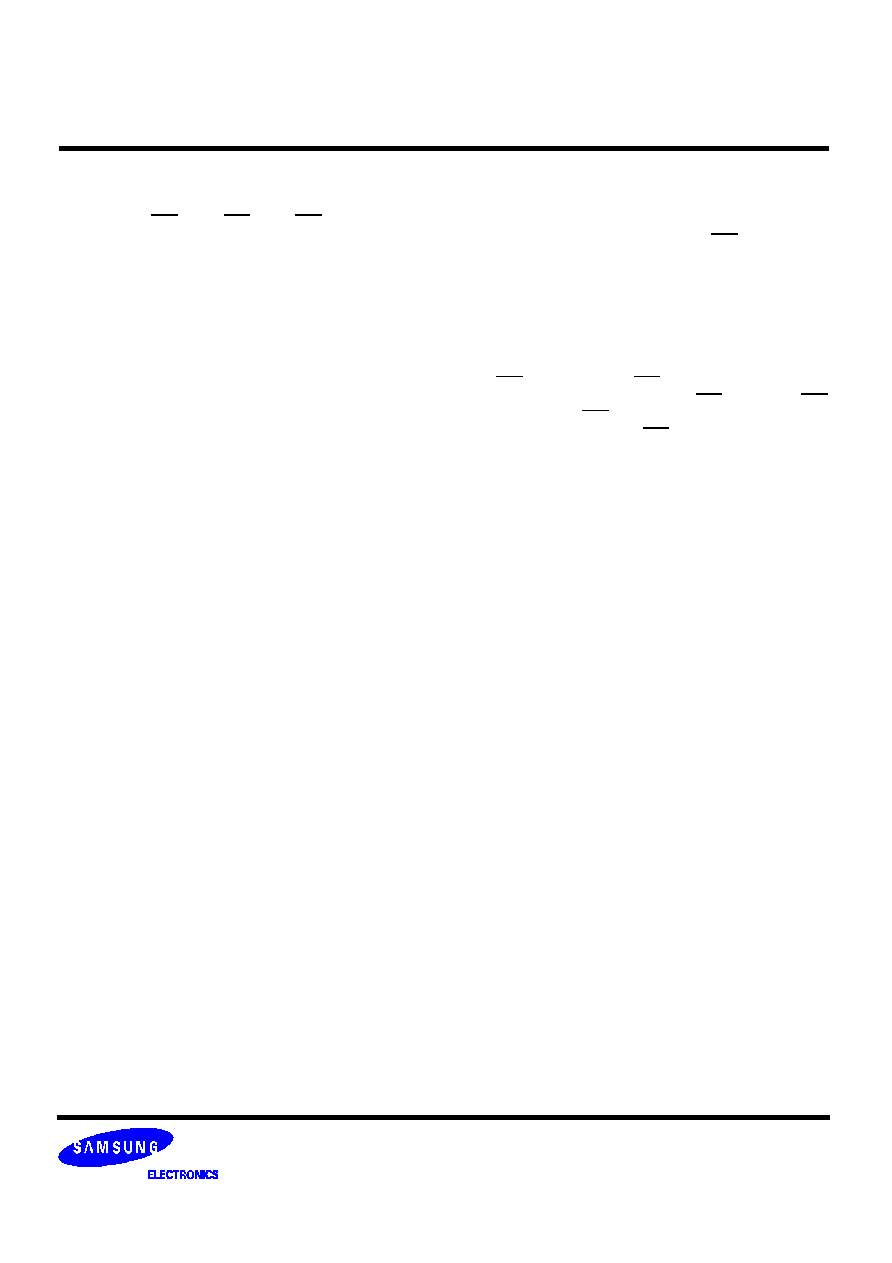
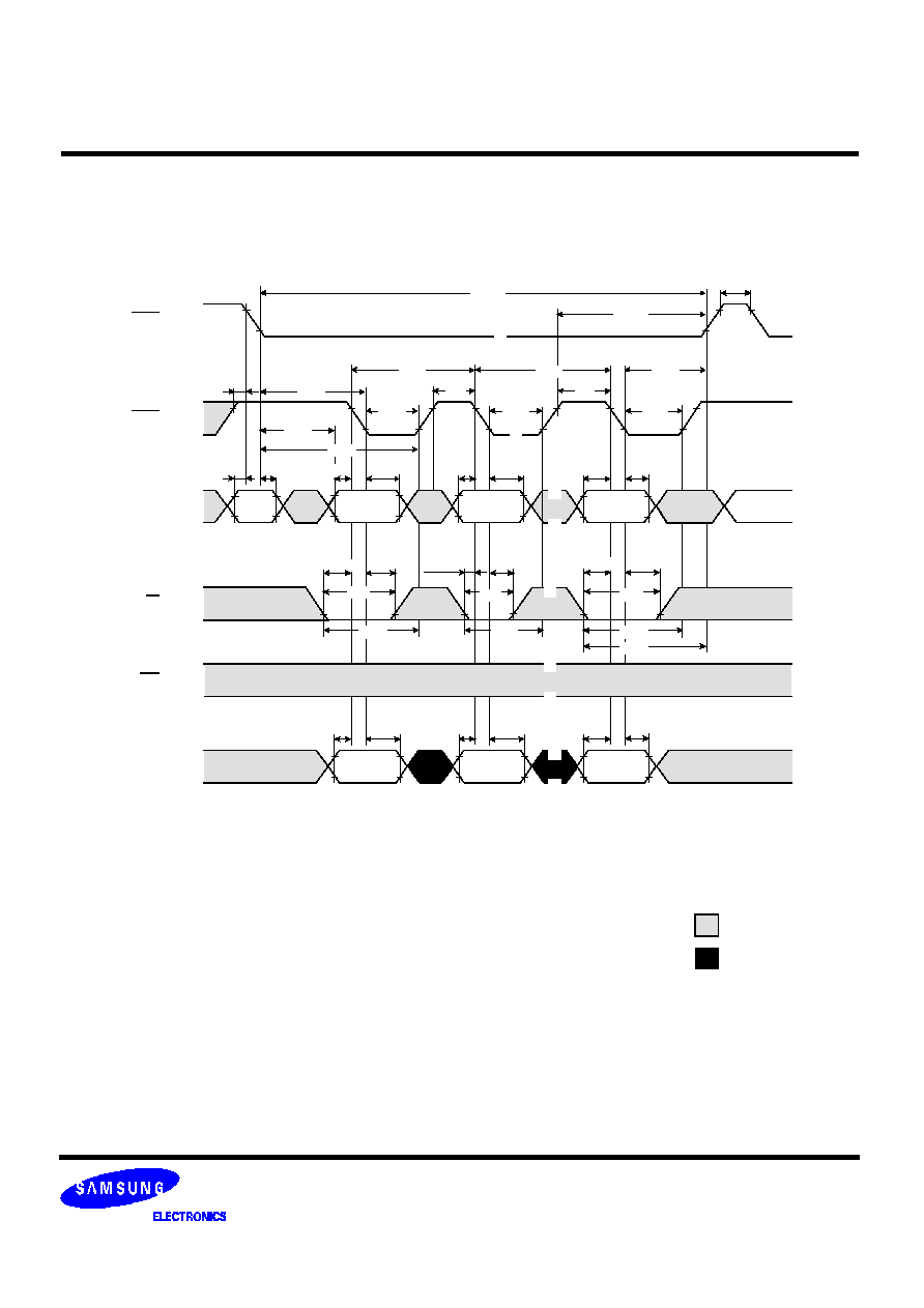
RAS
V
IH
-
V
IL
-
CAS
V
IH
-
V
IL
-
A
V
IH
-
V
IL
-
W
V
IH
-
V
IL
-
OE
V
IH
-
V
IL
-
V
OH
-
V
OL
-
COLUMN
ADDRESS
ROW
ADDRESS
t
RAS
t
RC
t
CRP
t
RP
t
CSH
t
RSH
t
RCD
t
CAS
t
RAL
t
ASR
t
RAH
t
ASC
t
CAH
t
CRP
t
AA
t
OEA
t
CLZ
t
RAC
OPEN
t
RCH
Don
t care
Undefined
t
RAD
t
RRH
DATA-OUT
t
REZ
t
RCS
READ CYCLE
t
OEZ
t
CEZ
t
WEZ
DQ
t
OLZ
t
CAC
DRAM MODULE
KMM372F320(8)0CS1
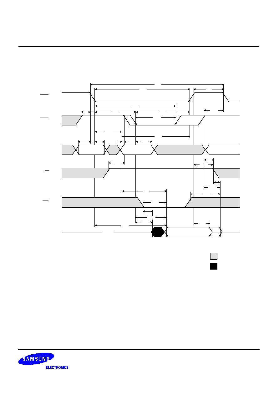
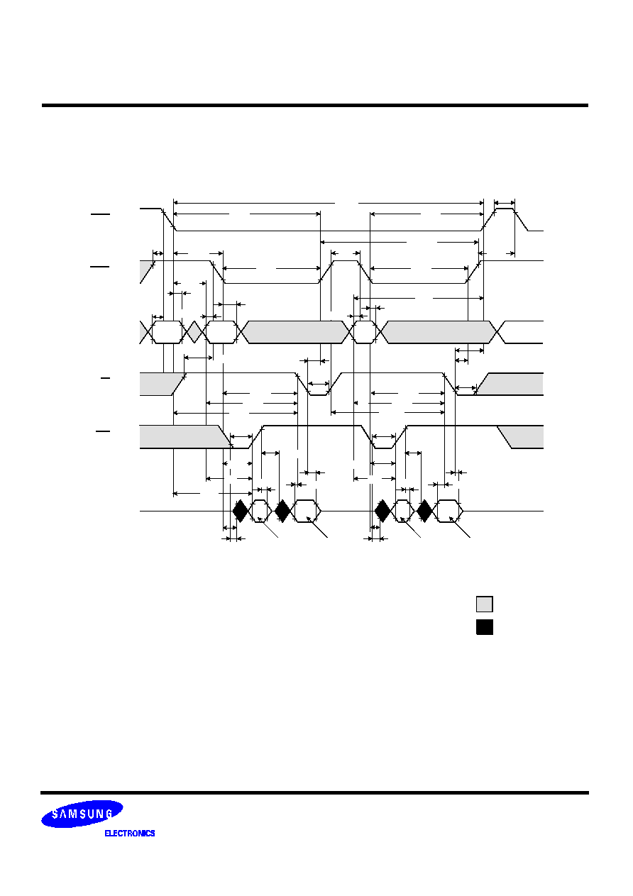
t
WCS
NOTE : D
OUT
= OPEN
WRITE CYCLE ( EARLY WRITE )
RAS
V
IH
-
V
IL
-
V
IH
-
V
IL
-
A
V
IH
-
V
IL
-
W
V
IH
-
V
IL
-
OE
V
IH
-
V
IL
-
V
IH
-
V
IL
-
COLUMN
ADDRESS
ROW
ADDRESS
t
RAS
t
RC
t
CRP
t
RP
t
CSH
t
RSH
t
RCD
t
CAS
t
RAL
t
RAD
t
ASR
t
RAH
t
ASC
t
CAH
t
CRP
Don
t care
Undefined
t
WCH
t
WP
CAS
t
RWL
t
CWL
t
DS
t
DH
DATA-IN
DQ

DRAM MODULE
KMM372F320(8)0CS1
NOTE : D
OUT
= OPEN
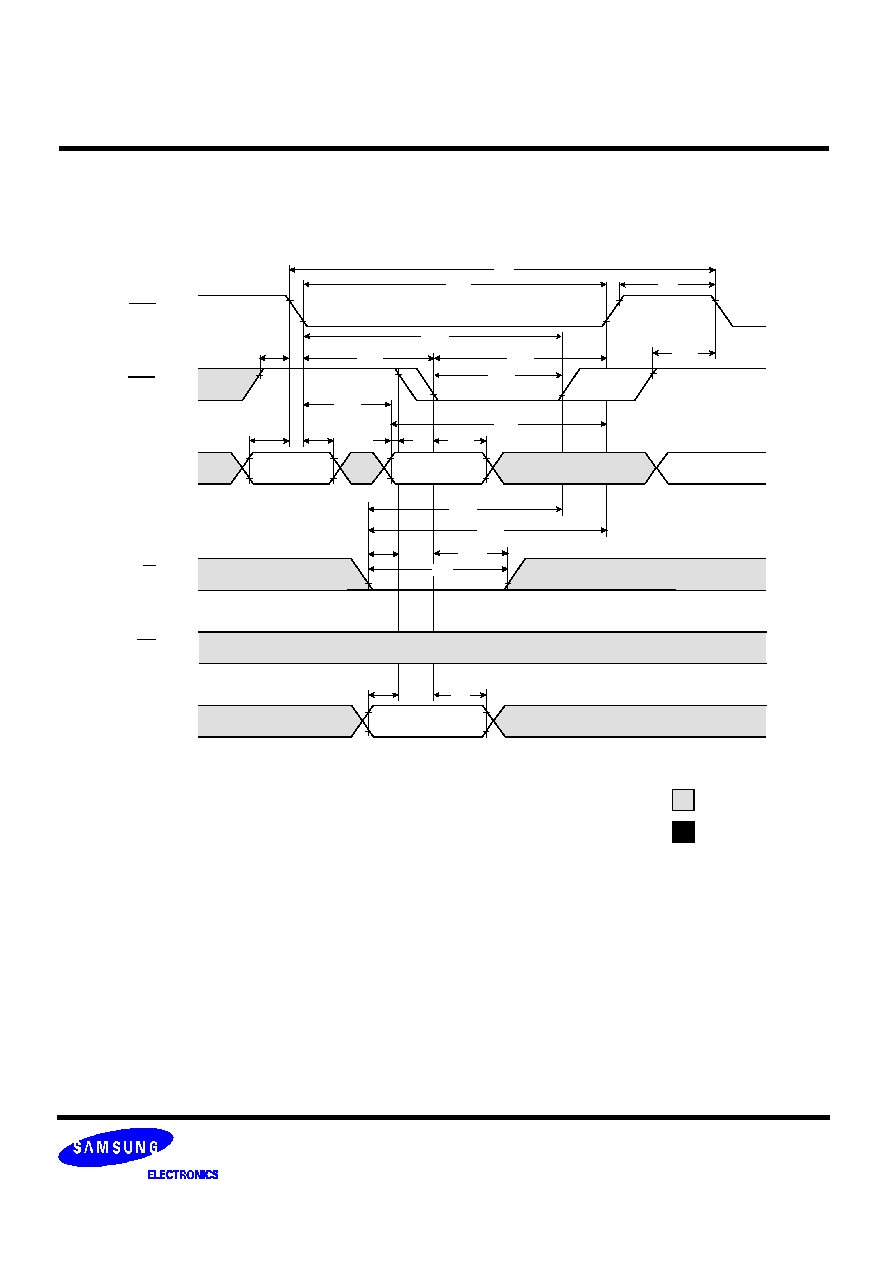
WRITE CYCLE ( OE CONTROLLED WRITE )
RAS
V
IH
-
V
IL
-
A
V
IH
-
V
IL
-
W
V
IH
-
V
IL
-
OE
V
IH
-
V
IL
-
V
IH
-
V
IL
-
DQ
COLUMN
ADDRESS
ROW
ADDRESS
t
RAS
t
RC
t
CRP
t
RP
t
CSH
t
RSH
t
RCD
t
CAS
t
RAL
t
RAD
t
ASR
t
RAH
t
ASC
t
CAH
t
CRP
t
WP
Don
t care
Undefined
CAS
V
IH
-
V
IL
-
t
RWL
t
CWL
t
DH
t
OEH
t
OED
DATA-IN
t
DS

DRAM MODULE
KMM372F320(8)0CS1
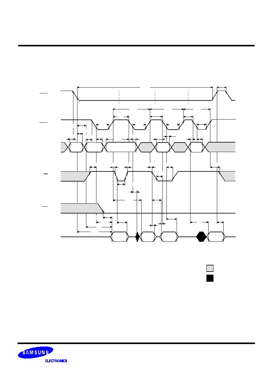
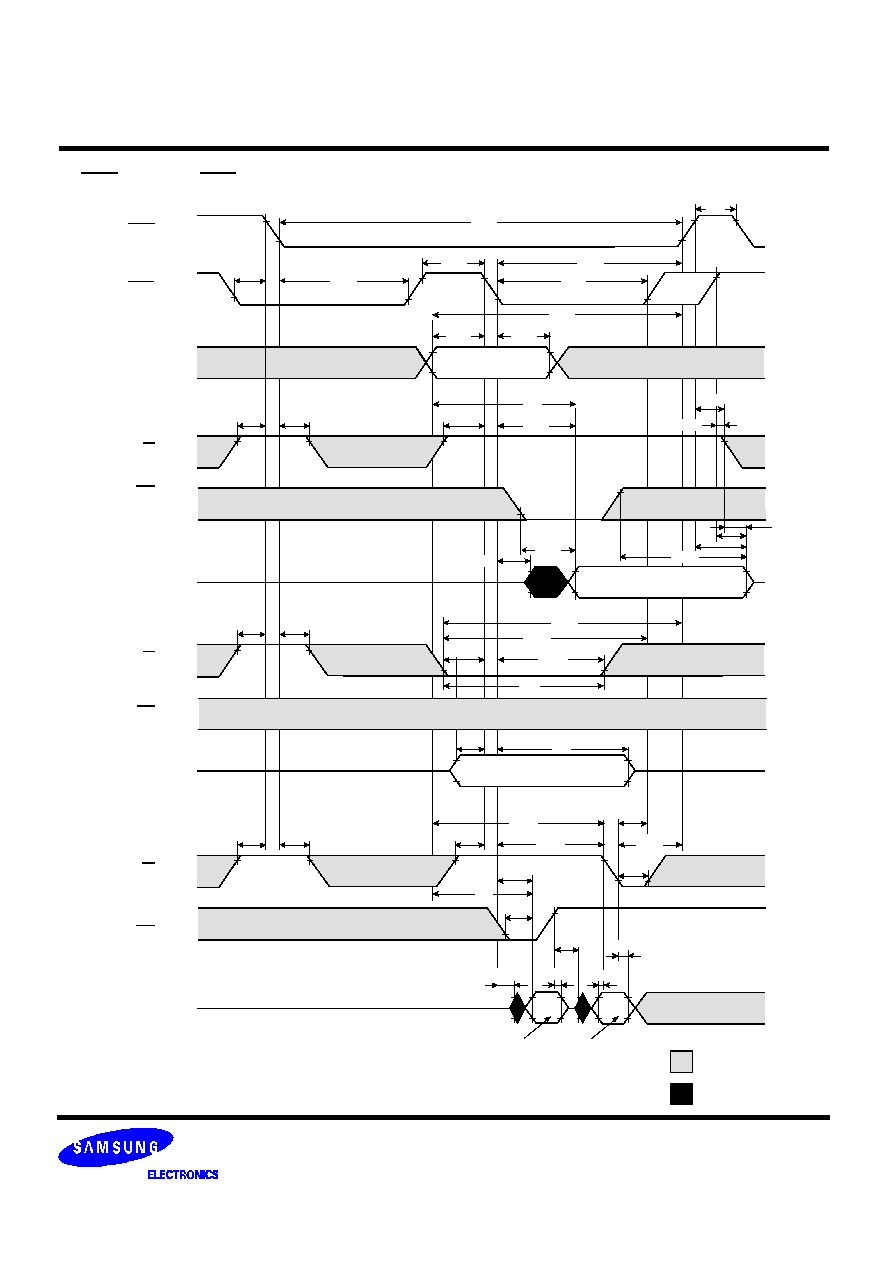
READ - MODIFY - WRITE CYCLE
RAS
V
IH
-
V
IL
-
CAS
V
IH
-
V
IL
-
A
V
IH
-
V
IL
-
W
V
IH
-
V
IL
-
OE
V
IH
-
V
IL
-
V
I/OH
-
V
I/OL
-
DQ
ROW
ADDR
t
RAS
t
RWC
t
RP
t
RSH
t
RCD
t
CAS
t
CSH
t
RAD
t
ASR
t
RAH
t
ASC
t
CAH
t
CRP
VALID
t
WP
Don
t care
t
RWL
t
CWL
t
OEZ
t
OEA
t
OED
t
AWD
t
CWD
t
RWD
DATA-OUT
Undefined
VALID
DATA-IN
t
RAC
t
AA
t
CAC
t
CLZ
t
DS
t
DH
COLUMN
ADDRESS
t
OLZ
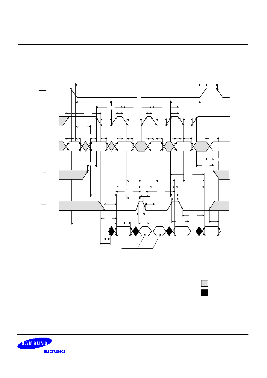
DRAM MODULE
KMM372F320(8)0CS1
t
DOH
HYPER PAGE READ CYCLE
RAS
V
IH
-
V
IL
-
CAS
V
IH
-
V
IL
-
A
V
IH
-
V
IL
-
W
V
IH
-
V
IL
-
OE
V
IH
-
V
IL
-
COLUMN
ADDRESS
ROW
ADDR
t
RASP
t
RP
t
RCD
t
ASR
t
CRP
Don
t care
Undefined
V
OH
-
V
OL
-
DQ
t
OEP
COLUMN
ADDRESS
t
CAS
t
CAS
t
CAS
t
CAS
t
CP
t
CP
t
CP
t
HPC
t
HPC
t
HPC
t
RHCP
t
CSH
t
RAD
t
RAH
t
ASC
t
CAH
t
CAH
t
CAH
t
ASC
t
CAH
t
RCS
t
AA
t
RCH
t
ASC
COLUMN
ADDRESS
COLUMN
ADDR
VALID
DATA-OUT
t
OEZ
t
OEA
t
OEP
t
AA
t
CAC
t
OEA
t
AA
t
CPA
t
CAC
t
CPA
VALID
DATA-OUT
VALID
DATA-OUT
t
OEZ
t
CLZ
t
RAC
t
OEA
t
OLZ
t
CAC
t
RRH
t
CHO
t
REZ
t
OEZ
t
CAC
t
OCH
t
CPA
t
CAC
VALID
DATA-OUT
°Û
t
ASC
t
AA
DRAM MODULE
KMM372F320(8)0CS1
RAS
V
IH
-
V
IL
-
CAS
V
IH
-
V
IL
-
A
V
IH
-
V
IL
-
W
V
IH
-
V
IL
-
OE
V
IH
-
V
IL
-
COLUMN
ADDRESS
ROW
ADDR.
t
RASP
t
RP
t
RCD
t
ASR
t
CRP
Don
t care
HYPER PAGE WRITE CYCLE ( EARLY WRITE )
Undefined
V
IH
-
V
IL
-
DQ
t
RHCP
t
RAD
t
RAH
t
CAH
t
CAH
t
ASC
t
CAH
t
ASC
VALID
DATA-IN
t
DS
°Û
COLUMN
ADDRESS
COLUMN
ADDRESS
t
CAS
t
CP
t
CAS
t
CP
t
CAS
t
RSH
°Û
t
CSH
t
ASC
°Û
°Û
t
WP
t
WCS
t
WCH
t
WP
t
WCS
t
WCH
t
WP
t
WCS
t
WCH
°Û
°Û
°Û
VALID
DATA-IN
VALID
DATA-IN
°Û
°Û
t
DH
t
DS
t
DH
t
DS
t
DH
t
CWL
t
CWL
t
CWL
t
RWL
NOTE : D
OUT
= OPEN
t
HPC
t
HPC
DRAM MODULE
KMM372F320(8)0CS1
Don
t care
HYPER PAGE READ-MODIFY-WRITE CYCLE
Undefined
RAS
V
IH
-
V
IL
-
CAS
V
IH
-
V
IL
-
A
V
IH
-
V
IL
-
W
V
IH
-
V
IL
-
OE
V
IH
-
V
IL
-
V
I/OH
-
V
I/OL
-
ROW
ADDR
t
CSH
t
RASP
t
RP
t
ASR
t
RAH
t
RCD
t
CP
t
RAD
t
CAH
t
WP
t
DH
COL.
ADDR
COL.
ADDR
t
CAS
t
CAS
t
CRP
t
ASC
t
CAH
t
RAL
t
RCS
t
CWL
t
CWD
t
AWD
t
RWD
t
WP
t
CWD
t
AWD
t
CWL
t
RAC
t
OEA
t
CLZ
t
OEZ
t
CPWD
t
OED
t
ASC
t
CLZ
t
OEA
t
CAC
t
AA
t
DH
t
OED
t
RWL
t
CRP
t
DS
t
OEZ
VALID
DATA-OUT
VALID
DATA-IN
VALID
DATA-OUT
VALID
DATA-IN
t
DS
DQ
t
RSH
t
OLZ
t
OLZ
t
HPRWC
t
CAC
t
AA
DRAM MODULE
KMM372F320(8)0CS1
HYPER PAGE READ AND WRITE MIXED CYCLE
RAS
V
IH
-
V
IL
-
CAS
V
IH
-
V
IL
-
A
V
IH
-
V
IL
-
W
V
IH
-
V
IL
-
OE
V
IH
-
V
IL
-
COLUMN
ADDRESS
ROW
ADDR
t
RASP
t
RP
Don
t care
Undefined
V
I/OH
-
V
I/OL
-
DQ
t
WEZ
t
CP
t
CP
t
HPC
t
HPC
t
HPC
t
RAD
t
RAH
t
ASC
t
CAH
t
CAH
t
CAH
t
ASC
t
CAH
t
RCH
t
RCS
t
RCS
t
RCH
t
ASC
COLUMN
ADDRESS
COL.
ADDR
VALID
DATA-OUT
t
REZ
t
AA
t
WCS
VALID
DATA-OUT
VALID
DATA-OUT
VALID
DATA-IN
t
RAC
COL.
ADDR
t
CAS
t
ASR
t
CAS
t
CAS
t
CAS
t
ASC
t
CP
t
RCH
t
WCH
t
WPE
t
CLZ
t
CPA
t
WED
t
AA
t
WEZ
t
DS
t
DH
t
CAC
t
OEA
READ(
t
CAC
)
READ(
t
CPA
)
WRITE
READ(
t
AA
)
DRAM MODULE
KMM372F320(8)0CS1
Don
t care
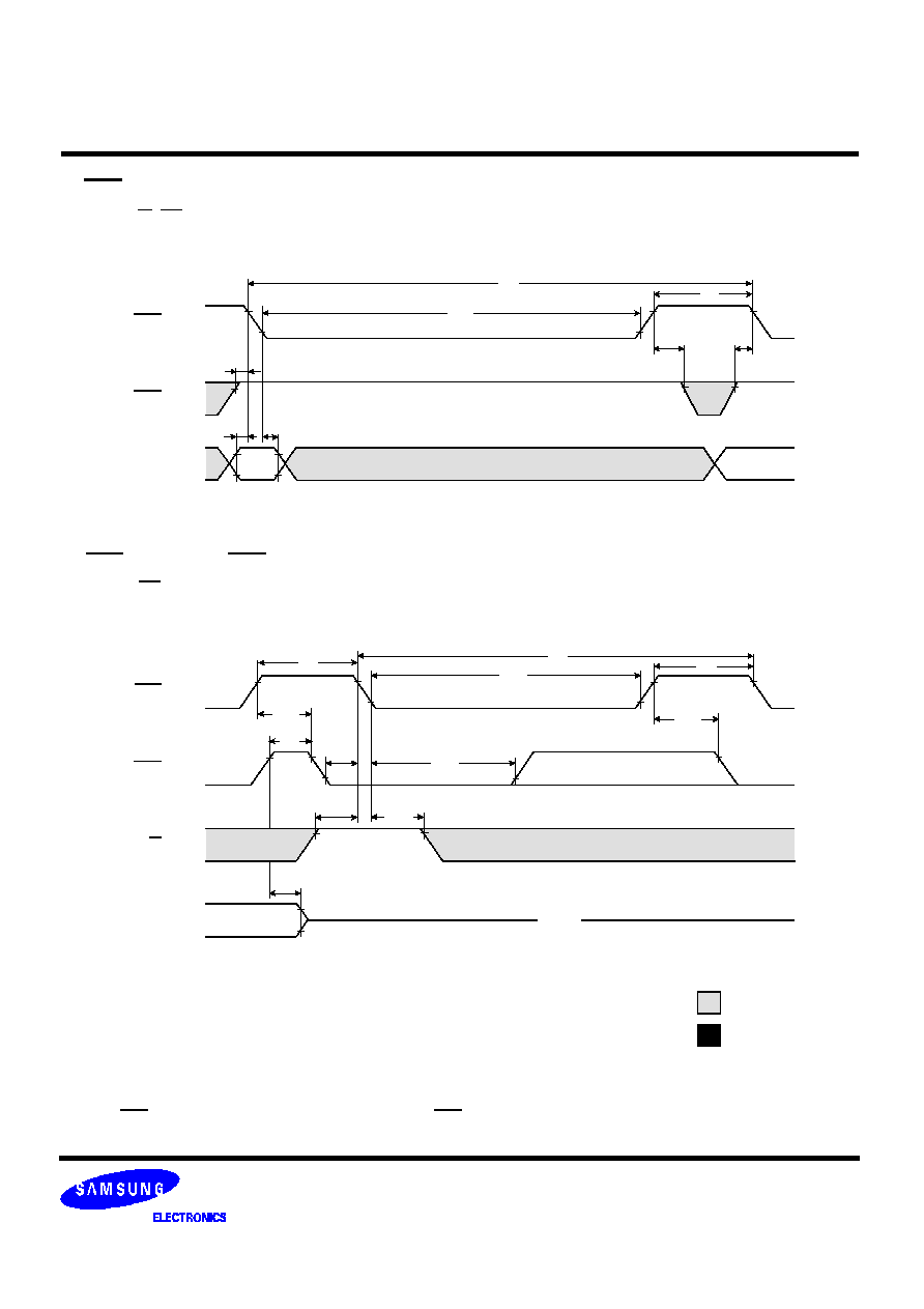
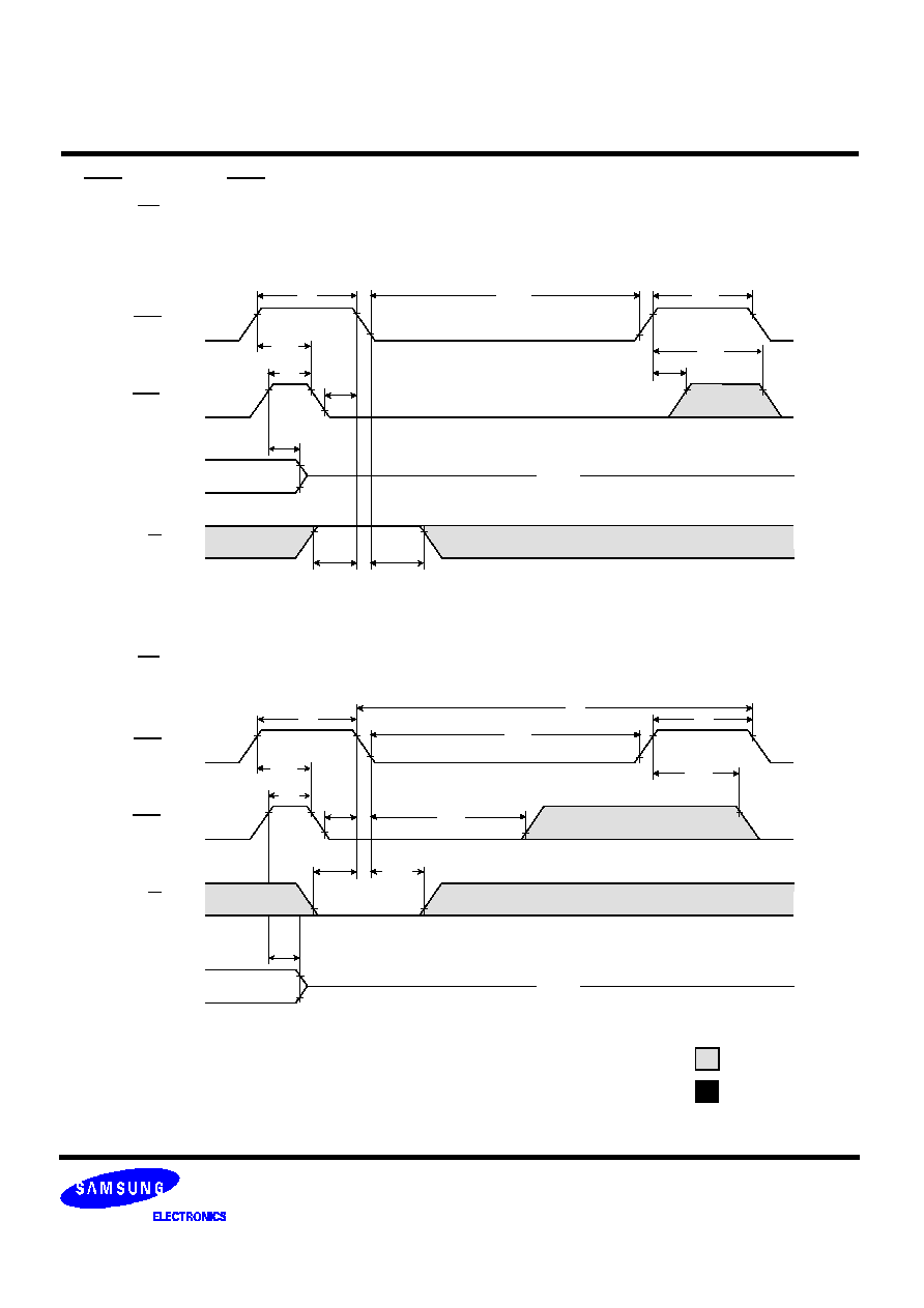
RAS - ONLY REFRESH CYCLE*
NOTE : W, OE, D
IN
= Don
t care
Undefined
D
OUT
= OPEN
RAS
V
IH
-
V
IL
-
CAS
V
IH
-
V
IL
-
A
V
IH
-
V
IL
-
ROW
ADDR
t
RC
t
RP
t
ASR
t
CRP
t
RAS
t
RAH
t
RPC
t
CRP
OPEN
CAS - BEFORE - RAS REFRESH CYCLE
NOTE : OE , A = Don
t care
RAS
V
IH
-
V
IL
-
CAS
V
IH
-
V
IL
-
t
RC
t
RP
t
RAS
t
RPC
t
CP
t
RPC
t
CSR
t
CHR
t
CEZ
V
OH
-
V
OL
-
DQ
t
WRP
t
WRH
W
V
IH
-
V
IL
-
t
RP
* In RAS-only refresh cycle of 64Mb A-dile & B-die, when CAS signal transits from Low to High, the valid data may be cut off.

DRAM MODULE
KMM372F320(8)0CS1
HIDDEN REFRESH CYCLE ( READ )
t
OEZ
DATA-OUT
t
RP
RAS
V
IH
-
V
IL
-
CAS
V
IH
-
V
IL
-
A
V
IH
-
V
IL
-
W
V
IH
-
V
IL
-
OE
V
IH
-
V
IL
-
ROW
ADDRESS
t
RAS
t
RC
t
CHR
t
RCD
t
RSH
t
RAD
t
ASR
t
RAH
t
ASC
t
CRP
Don
t care
Undefined
V
OH
-
V
OL
-
DQ
t
WRH
t
RRH
COLUMN
ADDRESS
t
OEA
t
RAS
t
RC
t
CAH
t
RCS
t
AA
t
RAC
t
CLZ
t
CAC
t
CEZ
OPEN
t
RP
t
WEZ
t
REZ
t
OLZ
t
WRP

DRAM MODULE
KMM372F320(8)0CS1
t
CRP
t
WCS
t
RP
RAS
V
IH
-
V
IL
-
A
V
IH
-
V
IL
-
W
V
IH
-
V
IL
-
OE
V
IH
-
V
IL
-
ROW
ADDRESS
t
RAS
t
RC
t
RAD
t
ASR
t
RAH
t
ASC
Don
t care
HIDDEN REFRESH CYCLE ( WRITE )
Undefined
CAS
V
IH
-
V
IL
-
V
IH
-
V
IL
-
DQ
t
RSH
t
RCD
t
WRH
COLUMN
ADDRESS
t
RAS
t
RC
t
CHR
t
CAH
t
WRP
t
DS
NOTE : D
OUT
= OPEN
t
WP
t
WCH
DATA-IN
t
DH
t
RP
DRAM MODULE
KMM372F320(8)0CS1
CAS-BEFORE-RAS REFRESH COUNTER TEST CYCLE
RAS
V
IH
-
V
IL
-
CAS
V
IH
-
V
IL
-
A
V
IH
-
V
IL
-
COLUMN
ADDRESS
t
RAS
t
RSH
t
CHR
t
RAL
t
CSR
t
CPT
t
RP
t
CAS
t
ASC
t
CAH
READ CYCLE
V
OH
-
V
OL
-
DATA-OUT
DQ
t
REZ
t
CLZ
WRITE CYCLE
V
IH
-
V
IL
-
DATA-IN
DQ
t
DH
t
DS
W
V
IH
-
V
IL
-
t
WP
t
CWD
t
CWL
t
RWL
READ-MODIFY-WRITE
t
AWD
V
IH
-
V
IL
-
OE
t
OEA
t
AA
t
CAC
t
DS
t
DH
VALID
DATA-OUT
V
I/OH
-
V
I/OL
-
DQ
Don
t care
Undefined
V
IH
-
V
IL
-
OE
t
OEA
t
OEZ
OE
V
IH
-
V
IL
-
t
RCS
t
CLZ
t
OEZ
t
OED
t
WRP
t
WRH
t
RRH
t
RCH
t
RCS
t
CAC
t
AA
V
IH
-
V
IL
-
W
t
WRP
t
WRH
t
WCS
t
WCH
t
CWL
V
IH
-
V
IL
-
W
t
WP
t
RWL
t
WRP
t
WRH
VALID
DATA-IN
NOTE : This timing diagram is applied to all devices besides 64M DRAM based modules.
t
CEZ
t
WEZ
DRAM MODULE
KMM372F320(8)0CS1
OPEN
CAS - BEFORE - RAS SELF REFRESH CYCLE
NOTE : OE, A = Don
t care
RAS
V
IH
-
V
IL
-
CAS
V
IH
-
V
IL
-
t
RPS
t
RASS
t
RPC
t
CP
t
RPC
t
CSR
t
CEZ
V
OH
-
V
OL
-
DQ
t
RP
Don
t care
Undefined
t
CHS
t
WRP
t
WRH
W
V
IH
-
V
IL
-
OPEN
TEST MODE IN CYCLE
NOTE : OE , A = Don
t care
RAS
V
IH
-
V
IL
-
CAS
V
IH
-
V
IL
-
t
RP
t
RC
t
RPC
t
CP
t
RPC
t
CSR
t
CEZ
V
OH
-
V
OL
-
DQ
t
WTS
t
WTH
W
V
IH
-
V
IL
-
t
CHR
t
RP
t
RAS
DRAM MODULE
KMM372F320(8)0CS1
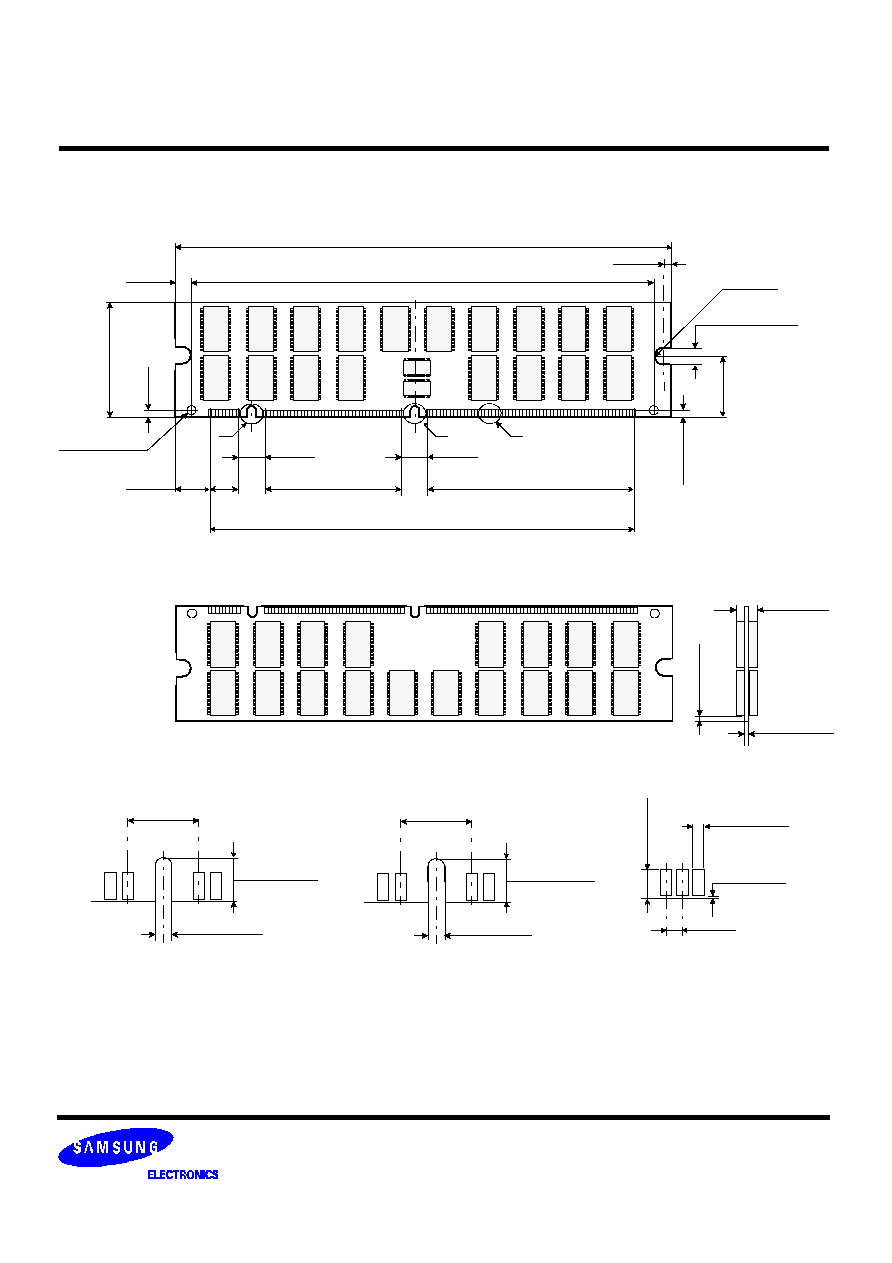
PACKAGE DIMENSIONS
Units : Inches (millimeters)
0.050
0.039
±
.002
0.01Max
(0.25 Max)
(1.000
±
.050)
(1.270)
0
.
1
0
0
M
i
n
(
2
.
5
4
0
M
i
n
)
Detail C
0.250
(6.350)
Detail A
0.1230
±
.0050
(3.125
±
.125)
Detail B
0.079
±
.0040
(2.000
±
.100)
Tolerances :
±
.005(.13) unless otherwise specified
The used device is 16Mx4 DRAM with EDO mode, TSOP II.
DRAM Part No. : KMM372F3200CS1 - KM44V16104CS.
KMM372F3280CS1 - KM44V16004CS.
0.250
(6.350)
0.1230
±
.0050
(3.125
±
.125)
0.079
±
.0040
(2.000
±
.100)
5.250
5.014
0.050
±
0.0039
(1.270
±
0.10)
R 0.079
(R 2.000)
0.250
(6.350)
1.450
(36.830)
2.150
(54.61)
0.350
0
.
1
0
0
M
i
n
(
2
.
5
4
0
M
i
n
)
0
.
7
0
0
(
1
7
.
7
8
0
)
.118DIA
±
.004
(3.000DIA
±
.100)
(8.890)
A
B
C
0.250
(6.350)
.450
(11.430)
4.550
(115.57)
0.157
±
0.004
(4.000
±
0.100)
0.054
(1.372)
(127.350)
(133.350)
2
.
1
0
0
(
5
3
.
3
4
)
0.118
(3.000)
0.150Max
(3.81Max)
0
.
1
1
8
(
3
.
0
0
0
)
0
.
1
6
5
M
i
n
(
4
.
1
9
M
i
n
)
( Back view )
( Front view )