
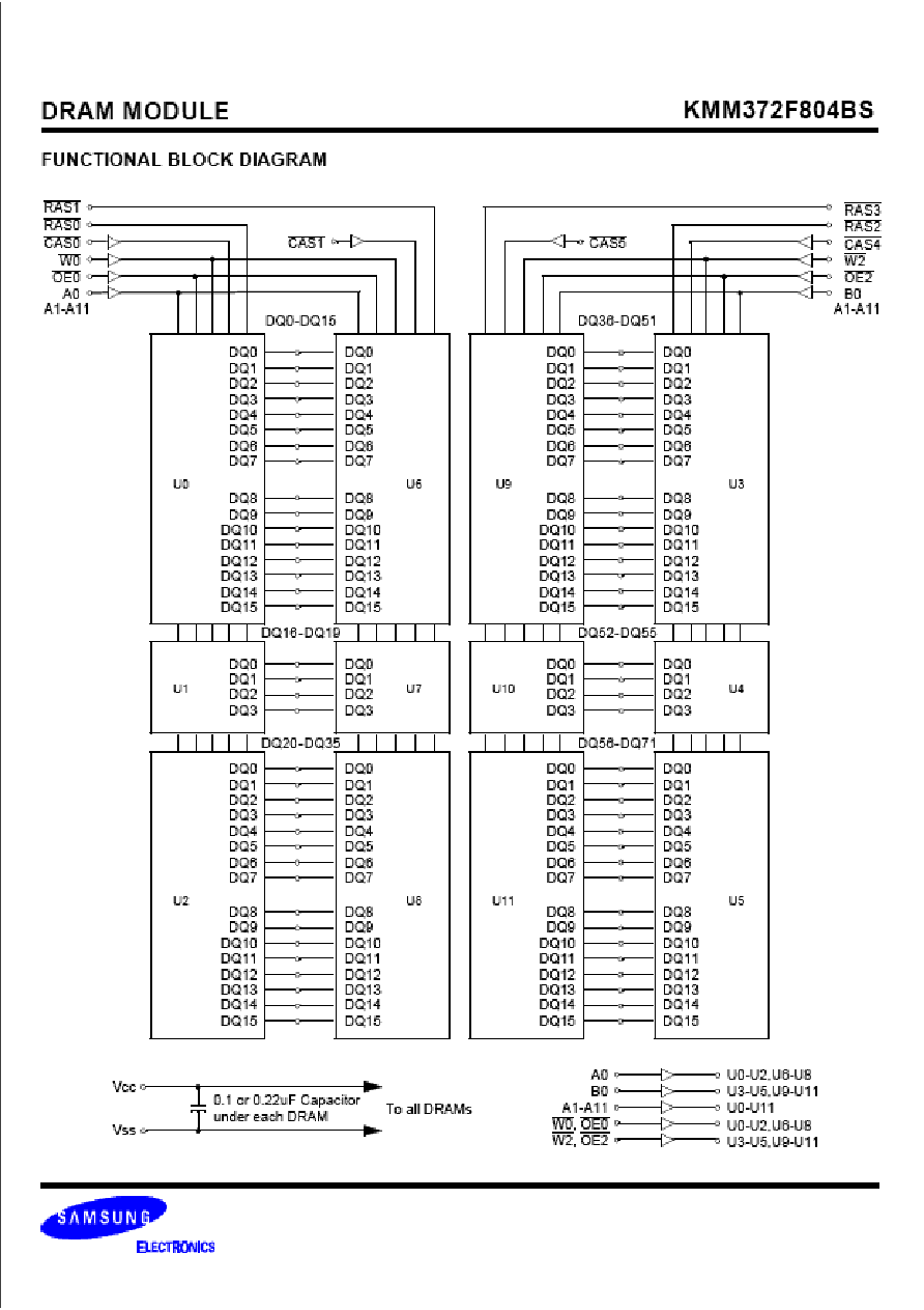

DRAM MODULE
KMM372F804BS
I
CC1
, I
CC3
, I
CC4
and I
CC6
are dependent on output loading and cycle rates. Specified values are obtained with the output open.
I
CC
is specified as an average current. In I
CC1
and I
CC3
, address can be changed maximum once while RAS=V
IL
. In I
CC4
,
address can be changed maximum once within one EDO mode cycle time, t
HPC
.
* NOTE :
ABSOLUTE MAXIMUM RATINGS *
* Permanent device damage may occur if ABSOLUTE MAXIMUM RATINGS are exceeded. Functional operation should be restricted to
the conditions as detailed in the operational sections of this data sheet. Exposure to absolute maximum rating conditions for intended
periods may affect device reliability.
Item
Symbol
Rating
Unit
Voltage on any pin relative V
SS
Voltage on V
CC
supply relative to V
SS
Storage Temperature
Power Dissipation
Short Circuit Output Current
V
IN
, V
OUT
V
CC
T
stg
P
D
I
OS
-0.5 to +4.6
-0.5 to +4.6
-55 to +125
12
50
V
V
�
C
W
mA
DC AND OPERATING CHARACTERISTICS
(Recommended operating conditions unless otherwise noted)
I
CC1
*
I
CC2
I
CC3
*
I
CC4
*
I
CC5
I
CC6
*
I(
IL)
I(
OL)
V
OH
V
OL
Symbol
Speed
KMM372F804BS
Unit
Min
Max
I
CC1
-5
-6
-
-
760
700
mA
mA
I
CC2
Don
t care
-
100
mA
I
CC3
-5
-6
-
-
760
700
mA
mA
I
CC4
-5
-6
-
-
700
640
mA
mA
I
CC5
Don
t care
-
30
mA
I
CC6
-5
-6
-
-
760
700
mA
mA
I
I(L)
I
O(L)
Don
t care
-10
-10
10
10
uA
uA
V
OH
V
OL
Don
t care
2.4
-
-
0.4
V
V
: Operating Current * (RAS, CAS, Address cycling @
t
RC
=min)
: Standby Current (RAS=CAS=W=V
IH
)
: RAS Only Refresh Current * (CAS=V
IH
, RAS cycling @
t
RC
=min)
: Extended Data Out Mode Current * (RAS=V
IL
, CAS cycling : t
HPC
=min)
: Standby Current (RAS=CAS=W=Vcc-0.2V)
: CAS-Before-RAS Refresh Current * (RAS and CAS cycling @
t
RC
=min)
: Input Leakage Current (Any input 0
V
IN
Vcc+0.3V, all other pins not under test=0 V)
: Output Leakage Current(Data Out is disabled, 0V
V
OUT
Vcc)
: Output High Voltage Level (I
OH
= -2mA)
: Output Low Voltage Level (I
OL
= 2mA)
RECOMMENDED OPERATING CONDITIONS
(Voltage referenced to V
SS
, T
A
= 0 to 70
�
C)
*1 : V
CC
+1.3V at pulse width
15ns, which is measured at V
CC
.
*2 : -1.3V at pulse width
15ns, which is measured at V
SS
.
Item
Symbol
Min
Typ
Max
Unit
Supply Voltage
Ground
Input High Voltage
Input Low Voltage
V
CC
V
SS
V
IH
V
IL
3.0
0
2.0
-0.3
*2
3.3
0
-
-
3.6
0
V
CC
+0.3
*1
0.8
V
V
V
V
DRAM MODULE
KMM372F804BS
CAPACITANCE
(T
A
= 25
�
C, f = 1MHz)
Item
Symbol
Min
Max
Unit
Input capacitance[A0, B0, A1 - A11]
Input capacitance[W0, W2, OE0, OE2]
Input capacitance[RAS0 - RAS3]
Input capacitance[CAS0, 1,4,5]
Input/Output capacitance[DQ0 - 71]
C
IN1
C
IN2
C
IN3
C
IN4
C
DQ
-
-
-
-
-
20
20
31
20
24
pF
pF
pF
pF
pF
Test condition : V
ih
/V
il
=2.2/0.7V, V
oh
/V
ol
=2.0/0.8V, output loading CL=100pF
Parameter
Symbol
-5
-6
Unit
Note
Min
Max
Min
Max
Random read or write cycle time
t
RC
84
104
ns
Read-modify-write cycle time
t
RWC
128
153
ns
Access time from RAS
t
RAC
50
60
ns
3,4,10
Access time from CAS
t
CAC
18
20
ns
3,4,5,13
Access time from column address
t
AA
30
35
ns
3,10,13
CAS to output in Low-Z
t
CLZ
8
8
ns
3,13
OE to output in Low-Z
t
OLZ
8
8
ns
3,13
Output buffer turn-off delay from CAS
t
CEZ
8
18
8
18
ns
6,11,13
Transition time(rise and fall)
t
T
1
50
1
50
ns
2
RAS precharge time
t
RP
30
40
ns
RAS pulse width
t
RAS
50
10K
60
10K
ns
RAS hold time
t
RSH
13
15
ns
13
CAS hold time
t
CSH
36
38
ns
13
CAS pulse width
t
CAS
8
10K
10
10K
ns
RAS to CAS delay time
t
RCD
15
32
18
40
ns
4,13
RAS to column address delay time
t
RAD
10
20
13
25
ns
10,13
CAS to RAS precharge time
t
CRP
10
10
ns
13
Row address set-up time
t
ASR
5
5
ns
13
Row address hold time
t
RAH
5
8
ns
13
Column address set-up time
t
ASC
0
0
ns
14
Column address hold time
t
CAH
7
10
ns
14
Column address to RAS lead time
t
RAL
30
35
ns
13
Read command set-up time
t
RCS
0
0
ns
Read command hold referenced to CAS
t
RCH
0
0
ns
8
Read command hold referenced to RAS
t
RRH
-2
-2
ns
8,13
Write command set-up time
t
WCS
0
0
ns
7
Write command hold time
t
WCH
7
10
ns
Write command pulse width
t
WP
7
10
ns
Write command to RAS lead time
t
RWL
13
15
ns
13
Write command to CAS lead time
t
CWL
7
10
ns
17
Data set-up time
t
DS
-2
-2
ns
9,13
Data hold time
t
DH
13
15
ns
9,13
Refresh period
t
REF
64
64
ms
CAS to W delay time
t
CWD
33
38
ns
7,16
RAS to W delay time
t
RWD
68
82
ns
7,13
AC CHARACTERISTICS
(0
�
C
T
A
70
�
C, V
CC
=3.3V
�
0.3V. See notes 1,2.)

DRAM MODULE
KMM372F804BS
AC CHARACTERISTICS
(0
�
C
T
A
70
�
C, V
CC
=3.3V
�
0.3V. See notes 1,2.)
Parameter
Symbol
-5
-6
Unit
Note
Min
Max
Min
Max
Column address to W delay time
t
AWD
45
53
ns
7
CAS precharge time to W delay time
t
CPWD
47
58
ns
CAS setup time(CAS-before-RAS refresh)
t
CSR
10
10
ns
13,18
CAS hold time(CAS-before-RAS refresh)
t
CHR
8
8
ns
13
RAS to CAS precharge time
t
RPC
3
3
ns
13
Access time from CAS precharge
t
CPA
33
40
ns
3,13
Hyper page cycle time
t
HPC
20
25
ns
12
Hyper page read-modify-write cycle time
t
HPRWC
70
77
ns
12
CAS precharge time(Hyper page cycle)
t
CP
7
10
ns
15
RAS pulse width (Hyper page cycle)
t
RASP
50
200K
60
200K
ns
RAS hold time from CAS precharge
t
RHCP
35
40
ns
13
W to RAS precharge time(C-B-R refresh)
t
WRP
15
15
ns
13
W to RAS hold time(C-B-R refresh)
t
WRH
8
8
ns
13
OE access time
t
OEA
18
20
ns
13
OE to data delay
t
OED
15
18
ns
13
Output buffer turn off delay time from OE
t
OEZ
8
18
8
18
ns
13
OE command hold time
t
OEH
5
5
ns
Output data hold time(C-B-R refresh)
t
DOH
10
10
ns
13
Output buffer turn off delay time from RAS
t
REZ
3
13
3
13
ns
6,11
Output buffer turn off delay time from W
t
WEZ
8
18
8
18
ns
6,13
W to data delay
t
WED
20
20
ns
13
OE to CAS hold time
t
OCH
5
5
ns
CAS hold time to OE
t
CHO
5
5
ns
OE precharge time
t
OEP
5
5
ns
W pulse width (Hyper page cycle)
t
WPE
5
5
ns
PDE to Valid PD bit
t
PD
10
10
ns
PDE to PD bit Inactive
t
PDOFF
2
7
2
7
ns
Present Detect Read Cycle