DRAM MODULE
KMM53232004BK/BKG
KMM53232004BK/BKG EDO Mode
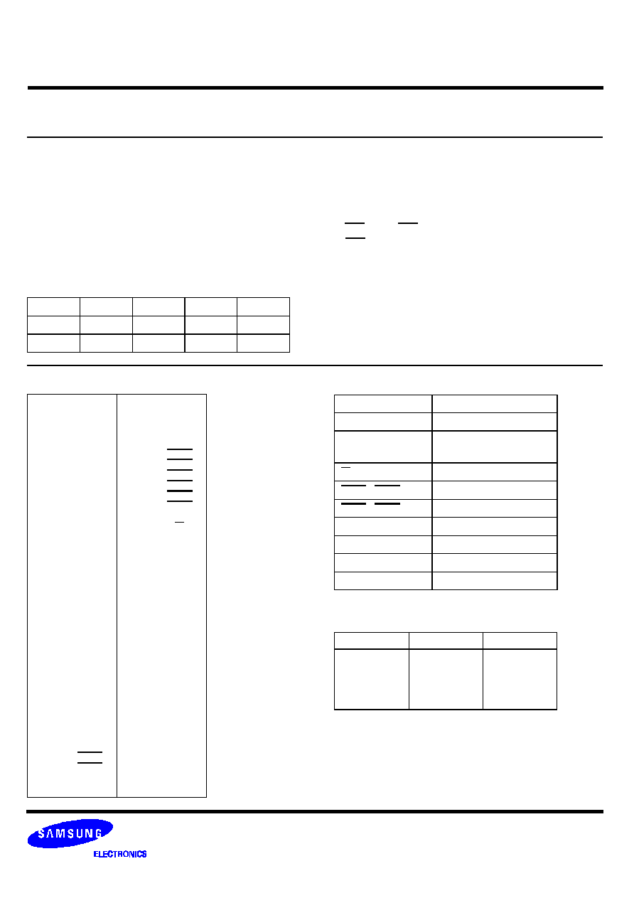
32M x 32 DRAM SIMM Using 16Mx4, 4K Refresh, 5V
The Samsung KMM53232004B is a 32Mx32bits Dynamic
RAM high density memory module. The Samsung
KMM53232004B consists of sixteen CMOS 16Mx4bits
DRAMs in SOJ packages mounted on a 72-pin glass-epoxy
substrate. A 0.1 or 0.22uF decoupling capacitor is mounted
on the printed circuit board for each DRAM. The
KMM53232004B is a Single In-line Memory Module with edge
connections and is intended for mounting into 72 pin edge
connector sockets.
∑ Part Identification
- KMM53232004BK(4K cycles/64ms Ref, SOJ, Solder)
- KMM53232004BKG(4K cycles/64ms Ref, SOJ, Gold)
∑ Extended Data Out Mode Operation
∑ CAS-before-RAS & Hidden Refresh capability
∑
RAS-only refresh capability
∑
TTL compatible inputs and outputs
∑
Single +5V
±
10% power supply
∑
JEDEC standard PDpin & pinout
∑
PCB : Height(1420mil), double sided component
GENERAL DESCRIPTION
FEATURES
PERFORMANCE RANGE
Speed
t
RAC
t
CAC
t
RC
t
HPC
-5
50ns
13ns
84ns
20ns
-6
60ns
15ns
104ns
25ns
PIN NAMES
Pin Name
Function
A0 - A11
Address Inputs
DQ0-7, DQ9-16
DQ18-25, DQ27-34
Data In/Out
W
Read/Write Enable
RAS0 - RAS3
Row Address Strobe
CAS0 - CAS3
Column Address Strobe
PD1 -PD4
Presence Detect
Vcc
Power(+5V)
Vss
Ground
NC
No Connection
PRESENCE DETECT PINS (Optional)
Pin
50NS
60NS
PD1
PD2
PD3
PD4
NC
Vss
Vss
Vss
NC
Vss
NC
NC
PIN CONFIGURATIONS
Pin
1
2
3
4
5
6
7
8
9
10
11
12
13
14
15
16
17
18
19
20
21
22
23
24
25
26
27
28
29
30
31
32
33
34
35
36
Symbol
V
SS
DQ0
DQ18
DQ1
DQ19
DQ2
DQ20
DQ3
DQ21
Vcc
NC
A0
A1
A2
A3
A4
A5
A6
A10
DQ4
DQ22
DQ5
DQ23
DQ6
DQ24
DQ7
DQ25
A7
A11
Vcc
A8
A9
RAS3
RAS2
NC
NC
Pin
37
38
39
40
41
42
43
44
45
46
47
48
49
50
51
52
53
54
55
56
57
58
59
60
61
62
63
64
65
66
67
68
69
70
71
72
Symbol
NC
NC
Vss
CAS0
CAS2
CAS3
CAS1
RAS0
RAS1
NC
W
NC
DQ9
DQ27
DQ10
DQ28
DQ11
DQ29
DQ12
DQ30
DQ13
DQ31
Vcc
DQ32
DQ14
DQ33
DQ15
DQ34
DQ16
NC
PD1
PD2
PD3
PD4
NC
Vss
SAMSUNG ELECTRONICS CO., LTD. reserves the right to
change products and specifications without notice.

DRAM MODULE
KMM53232004BK/BKG
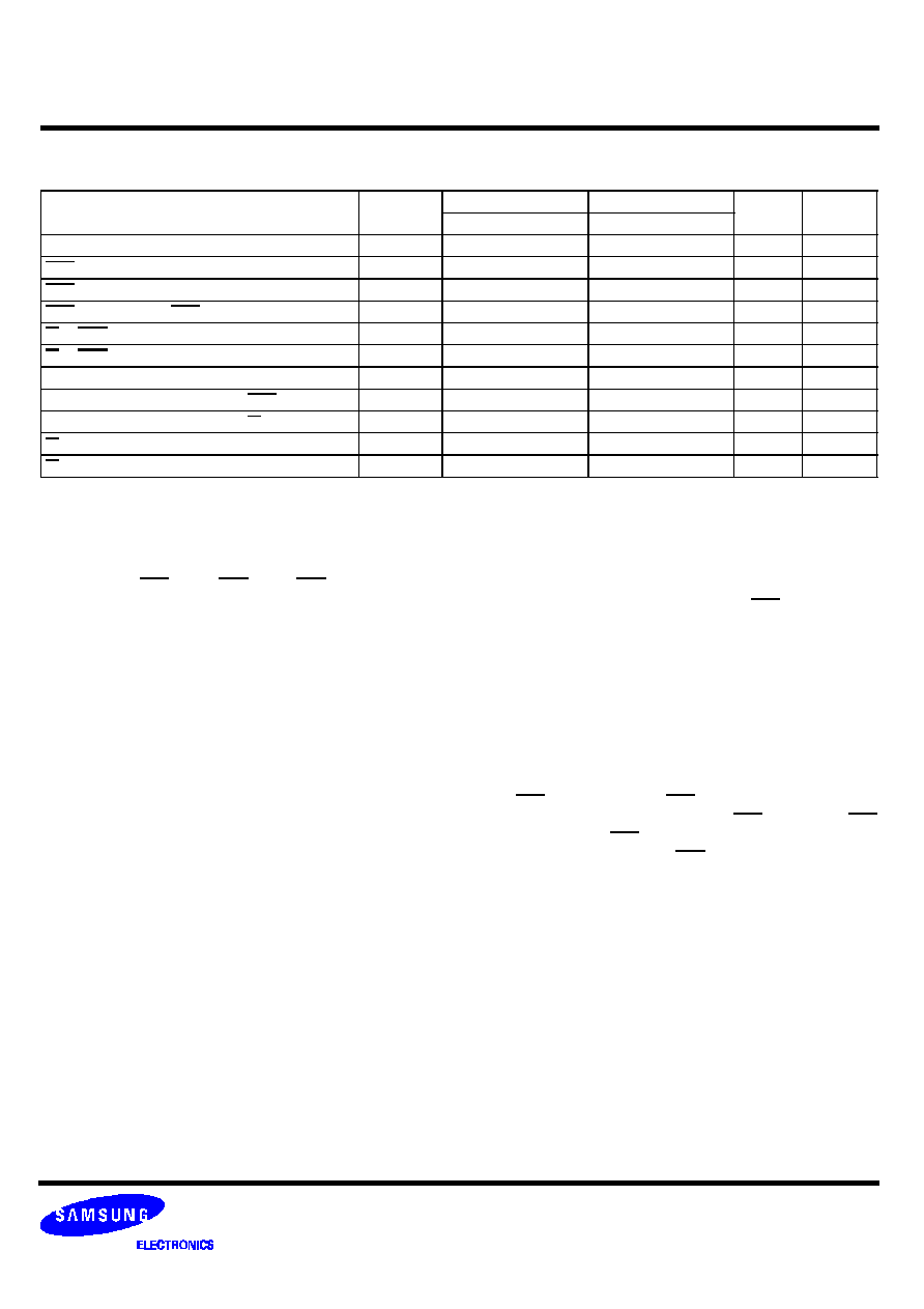
FUNCTIONAL BLOCK DIAGRAM
CAS
RAS
OE
DQ1
DQ2
DQ3
DQ4
W A0-A11
CAS0
RAS0
U0
Vcc
Vss
0.1 or 0.22uF Capacitor
for each DRAM
CAS
RAS
OE
DQ1
DQ2
DQ3
DQ4
W A0-A11
U1
CAS
RAS
OE
DQ1
DQ2
DQ3
DQ4
W A0-A11
U2
CAS
RAS
OE
DQ1
DQ2
DQ3
DQ4
W A0-A11
U3
CAS
RAS
OE
DQ1
DQ2
DQ3
DQ4
W A0-A11
U4
CAS
RAS
OE
DQ1
DQ2
DQ3
DQ4
W A0-A11
U5
CAS
RAS
OE
DQ1
DQ2
DQ3
DQ4
W A0-A11
U6
CAS
RAS
OE
DQ1
DQ2
DQ3
DQ4
W A0-A11
U7
To all DRAMs
CAS1
CAS2
RAS2
CAS3
W
A0-A11
CAS
RAS
OE
DQ1
DQ2
DQ3
DQ4
W A0-A11
CAS0
RAS1
U8
CAS
RAS
OE
DQ1
DQ2
DQ3
DQ4
W A0-A11
U9
CAS
RAS
OE
DQ1
DQ2
DQ3
DQ4
W A0-A11
U10
CAS
RAS
OE
DQ1
DQ2
DQ3
DQ4
W A0-A11
U11
CAS
RAS
OE
DQ1
DQ2
DQ3
DQ4
W A0-A11
U12
CAS
RAS
OE
DQ1
DQ2
DQ3
DQ4
W A0-A11
U13
CAS
RAS
OE
DQ1
DQ2
DQ3
DQ4
W A0-A11
U14
CAS
RAS
OE
DQ1
DQ2
DQ3
DQ4
W A0-A11
U15
CAS1
CAS2
RAS3
CAS3
DQ0~DQ3
DQ4~DQ7
DQ9~DQ12
DQ13~DQ16
DQ18~DQ21
DQ22~DQ25
DQ27~DQ30
DQ31~DQ34
DRAM MODULE
KMM53232004BK/BKG
I
CC1
, I
CC3
, I
CC4
and I
CC6
are dependent on output loading and cycle rates. Specified values are obtained with the output open.
I
CC
is specified as an average current. In I
CC1
and I
CC3
, address can be changed maximum once while RAS=V
IL
. In I
CC4
,
address can be changed maximum once within one EDO mode cycle time,
t
HPC
.
* NOTE :
ABSOLUTE MAXIMUM RATINGS *
* Permanent device damage may occur if ABSOLUTE MAXIMUM RATINGS are exceeded. Functional operation should be restricted to
the conditions as detailed in the operational sections of this data sheet. Exposure to absolute maximum rating conditions for intended
periods may affect device reliability.
Item
Symbol
Rating
Unit
Voltage on any pin relative to V
SS
Voltage on V
CC
supply relative to V
SS
Storage Temperature
Power Dissipation
Short Circuit Output Current
V
IN
, V
OUT
V
CC
T
stg
P
d
I
OS
-1 to +7.0
-1 to +7.0
-55 to +125
16
50
V
V
∞
C
W
mA
RECOMMENDED OPERATING CONDITIONS
(Voltage referenced to V
SS
, T
A
= 0 to 70
∞
C)
*1 : V
CC
+2.0V at pulse width
20ns, which is measured at V
CC
.
*2 : -2.0V at pulse width
20ns, whcih is measured at V
SS
.
Item
Symbol
Min
Typ
Max
Unit
Supply Voltage
Ground
Input High Voltage
Input Low Voltage
V
CC
V
SS
V
IH
V
IL
4.5
0
2.4
-1.0
*2
5.0
0
-
-
5.5
0
V
CC*1
0.8
V
V
V
V
DC AND OPERATING CHARACTERISTICS
(Recommended operating conditions unless otherwise noted)
I
CC1
I
CC2
I
CC3
I
CC4
I
CC5
I
CC6
I(
IL)
I(
OL)
V
OH
V
OL
Symbol
Speed
KMM53232004BK/BKG
Unit
Min
Max
I
CC1
-5
-6
-
-
976
896
mA
mA
I
CC2
Don
t care
-
32
mA
I
CC3
-5
-6
-
-
976
896
mA
mA
I
CC4
-5
-6
-
-
896
816
mA
mA
I
CC5
Don
t care
-
16
mA
I
CC6
-5
-6
-
-
976
896
mA
mA
I
I(L)
I
O(L)
Don
t care
-10
-10
10
10
uA
uA
V
OH
V
OL
Don
t care
2.4
-
-
0.4
V
V
: Operating Current * (RAS, CAS, Address cycling @
t
RC
=min)
: Standby Current (RAS=CAS=W=V
IH
)
: RAS Only Refresh Current * (CAS=V
IH
, RAS cycling @
t
RC
=min)
: Hyper Page Mode Current * (RAS=V
IL
, CAS cycling :
t
HPC
=min)
: Standby Current (RAS=CAS=W=Vcc-0.2V)
: CAS-Before-RAS Refresh Current * (RAS and CAS cycling @
t
RC
=min)
: Input Leakage Current (Any input 0
V
IN
Vcc+0.5V, all other pins not under test=0 V)
: Output Leakage Current(Data Out is disabled, 0V
V
OUT
Vcc)
: Output High Voltage Level (I
OH
= -5mA)
: Output Low Voltage Level (I
OL
= 4.2mA)
DRAM MODULE
KMM53232004BK/BKG
CAPACITANCE
(T
A
= 25
∞
C, V
CC
=5V, f = 1MHz)
Item
Symbol
Min
Max
Unit
Input capacitance[A0-A11]
Input capacitance[W]
Input capacitance[RAS0 - RAS3]
Input capacitance[CAS0 - CAS3]
Input/Output capacitance[DQ0-7, 9-16,18-25, 27-34]
C
IN1
C
IN2
C
IN3
C
IN4
C
DQ
-
-
-
-
-
90
122
38
38
17
pF
pF
pF
pF
pF
AC CHARACTERISTICS
(0
∞
C
T
A
70
∞
C, Vcc=5.0V
±
10%. See notes 1,2.)
Test condition : V
ih
/V
il
=2.4/0.8V, V
oh
/V
ol
=2.0/0.8V, output loading CL=100pF
Parameter
Symbol
-5
-6
Unit
Note
Min
Max
Min
Max
Random read or write cycle time
t
RC
84
104
ns
Access time from RAS
t
RAC
50
60
ns
3,4,10
Access time from CAS
t
CAC
13
15
ns
3,4,5
Access time from column address
t
AA
25
30
ns
3,10
CAS to output in Low-Z
t
CLZ
3
3
ns
3
Output buffer turn-off delay from CAS
t
CEZ
3
13
3
13
ns
6,12
Transition time(rise and fall)
t
T
1
50
1
50
ns
2
RAS precharge time
t
RP
30
40
ns
RAS pulse width
t
RAS
50
10K
60
10K
ns
RAS hold time
t
RSH
13
15
ns
CAS hold time
t
CSH
38
45
ns
CAS pulse width
t
CAS
8
10K
10
10K
ns
4
RAS to CAS delay time
t
RCD
20
37
20
45
ns
9
RAS to column address delay time
t
RAD
15
25
15
30
ns
CAS to RAS precharge time
t
CRP
5
5
ns
Row address set-up time
t
ASR
0
0
ns
Row address hold time
t
RAH
10
10
ns
Column address set-up time
t
ASC
0
0
ns
Column address hold time
t
CAH
8
10
ns
Column address to RAS lead time
t
RAL
25
30
ns
Read command set-up time
t
RCS
0
0
ns
Read command hold referenced to CAS
t
RCH
0
0
ns
8
Read command hold referenced to RAS
t
RRH
0
0
ns
8
Write command set-up time
t
WCS
0
0
ns
7
Write command hold time
t
WCH
10
10
ns
Write command pulse width
t
WP
10
10
ns
Write command to RAS lead time
t
RWL
13
15
ns
Write command to CAS lead time
t
CWL
8
10
ns
Data set-up time
t
DS
0
0
ns
9
Data hold time
t
DH
8
10
ns
9
Refresh period
t
REF
64
64
ms
CAS setup time (CAS-before-RAS refresh)
t
CSR
5
5
ns
CAS hold time (CAS-before-RAS refresh)
t
CHR
10
10
ns
RAS to CAS precharge time
t
RPC
5
5
ns
Access time from CAS precharge
t
CPA
28
35
ns
3
DRAM MODULE
KMM53232004BK/BKG
Test condition : V
ih
/V
il
=2.4/0.8V, V
oh
/V
ol
=2.0/0.8V, output loading CL=100pF
Parameter
Symbol
-5
-6
Unit
Note
Min
Max
Min
Max
Hyper page mode cycle time
t
HPC
20
25
ns
11
CAS precharge time (Hyper page cycle)
t
CP
8
10
ns
RAS pulse width (Hyper page cycle)
t
RASP
50
200K
60
200K
ns
RAS hold time from CAS precharge
t
RHCP
30
35
ns
W to RAS precharge time(C-B-R refresh)
t
WRP
10
10
ns
W to RAS hold time(C-B-R refresh)
t
WRH
10
10
ns
Output data hold time
t
DOH
5
5
ns
Output buffer turn off delay from RAS
t
REZ
3
13
3
15
ns
6,12
Output buffer turn off delay from W
t
WEZ
3
13
3
15
ns
6
W to data delay
t
WED
15
15
ns
W pulse width
t
WPE
5
5
ns
AC CHARACTERISTICS
(0
∞
C
T
A
70
∞
C, Vcc=5.0V
±
10%. See notes 1,2.)
NOTES
An initial pause of 200us is required after power-up followed
by any 8 RAS-only or CAS-before-RAS refresh cycles before
proper device operation is achieved.
Input voltage levels are V
ih
/V
il
. V
IH
(min) and V
IL
(max) are ref-
erence levels for measuring timing of input signals. Transi-
tion times are measured between V
IH
(min) and V
IL
(max) and
are assumed to be 5ns for all inputs.
Measured with a load equivalent to 2 TTL loads and 100pF.
Operation within the
t
RCD
(max) limit insures that
t
RAC
(max)
can be met.
t
RCD
(max) is specified as a reference point only.
If
t
RCD
is greater than the specified
t
RCD
(max) limit, then
access time is controlled exclusively by
t
CAC
.
Assumes that
t
RCD
t
RCD
(max).
This parameter defines the time at which the output achieves
the open circuit and is not referenced for V
OH
or V
OL.
t
WCS
is non-restrictive operating parameter. It is included in
the data sheet as electrical characteristics only. If
t
WCS
t
WCS
(min), the cycle is an early write cycle and the
data out pin will remain high impedance for the duration of
the cycle.
Either
t
RCH
or
t
RRH
must be satisfied for a read cycle.
These parameters are referenced to the CAS leading edge in
early write cycles.
Operation within the
t
RAD
(max) limit insures that
t
RAC
(max)
can be met.
t
RAD
(max) is specified as reference point only. If
t
RAD
is greater than the specified
t
RAD
(max) limit access time
is controlled by
t
AA
.
t
ASC
6ns, Assume t
T
=2.0ns.
If RAS goes high before CAS high going, the open circuit
condition of the output is achieved by CAS high going. If CAS
goes high before RAS high going , the open circuit condition
of the output is achieved by RAS going.
1.
2.
3.
4.
5.
6.
7.
8.
9.
10.
11.
12.