Page 1
Rev.0.9 Apr. 1999
4/6/8/12/16d RIMM
TM
Module with 128Mb RDRAMs
KMMR18R84(6/8/C/G)C
KMMR16R84(6/8/C/G)C
4/6/8/12/16d RIMM
TM
Module with 144Mb RDRAMs
Preliminary
Overview
The Rambus
Æ
RIMMTM module is a general purpose high-
performance memory subsystem suitable for use in a broad
range of applications including computer memory, personal
computers, workstations, and other applications where high
bandwidth and low latency are required.
The Rambus RIMM module consists of 128Mb/144Mb
Direct Rambus DRAM devices. These are extremely high-
speed CMOS DRAMs organized as 8M words by 16 or 18
bits. The use of Rambus Signaling Level (RSL) technology
permits 600MHz or 800MHz transfer rates while using
conventional system and board design technologies.
RDRAM devices are capable of sustained data transfers at
1.25 ns per two bytes (10ns per 16 bytes).
The RDRAM architecture enables the highest sustained
bandwidth for multiple, simultaneous, randomly addressed,
memory transactions. The separate control and data buses
with independent row and column control yield over 95%
bus efficiency. The RDRAM's 32-banks architecture
supports up to four simultaneous transactions per device.
Features
High speed 800 and 600MHz RDRAM storage
184 edge connector pads with 1mm pad spacing
Maximum module PCB size : 133.5mm x 34.93mm x
1.37mm (5.21
"
x 1.375
"
x 0.05
"
)
Each RDRAM has 32 banks, for a total of 512, 384, 256,
192, or 128 banks on each 256/288MB, 192/216MB,
128/144MB, 96/108MB, or 64/72MB module respectively
Gold plated edge connector pad contacts
Serial Presence Detect(SPD) support
Operates from a 2.5 volt supply (±5%)
Low power and powerdown self refresh modes
Separate Row and Column buses for higher efficiency
RDRAMs use
µ-
BGA package type
Key Timing Parameters/Part Numbers
The following table lists the frequency and latency bins
available from RIMM modules. An optional ` S' designator
instead of `R' followed by ` hyphen(-)' indicates low power
modules.
TABLE 1. Part Number by Freq. & Latency
Form Factor
The Rambus RIMM modules are offered in a 184-pad 1mm
edge connector pad pitch form factor suitable for 184 contact
RIMM connectors. The RIMM module is suitable for
desktop and other system applications.
Organization
Speed
Part Number
a
a. -S designator is used for modules with lower self-refresh current.
Binning
I/O
Freq.
MHz
t
rac
(Row
Access
Time) ns
32M x 16/18
-RG6
600
53
KMMR16/18R84C-RG6
-RK8
800
45
KMMR16/18R84C-RK8
-RM8
800
40
KMMR16/18R84C-RM8
48M x 16/18
-RG6
600
53
KMMR16/18R86C-RG6
-RK8
800
45
KMMR16/18R86C-RK8
-RM8
800
40
KMMR16/18R86C-RM8
64M x 16/18
-RG6
600
53
KMMR16/18R88C-RG6
-RK8
800
45
KMMR16/18R88C-RK8
-RM8
800
40
KMMR16/18R88C-RM8
96M x 16/18
-RG6
600
53
KMMR16/18R8CC-RG6
-RK8
800
45
KMMR16/18R8CC-RK8
-RM8
800
40
KMMR16/18R8CC-RM8
128M x 16/18
-RG6
600
53
KMMR16/18R8GC-RG6
-RK8
800
45
KMMR16/18R8GC-RK8
-RM8
800
40
KMMR16/18R8GC-RM8
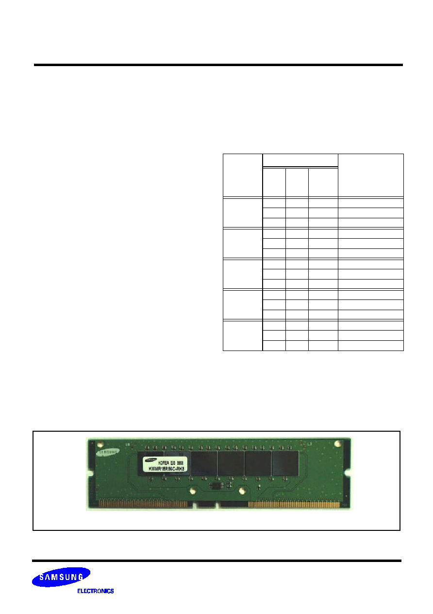
Figure 1: Rambus RIMM Module without heat spreader
Note: On two sided modules, RDRAMs are also installed on bottem side of PCB.
Page 2
4/6/8/12/16d RIMM
TM
Module with 128Mb RDRAMs
KMMR18R84(6/8/C/G)C
KMMR16R84(6/8/C/G)C
4/6/8/12/16d RIMM
TM
Module with 144Mb RDRAMs
Preliminary
Rev.0.9 Apr. 1999
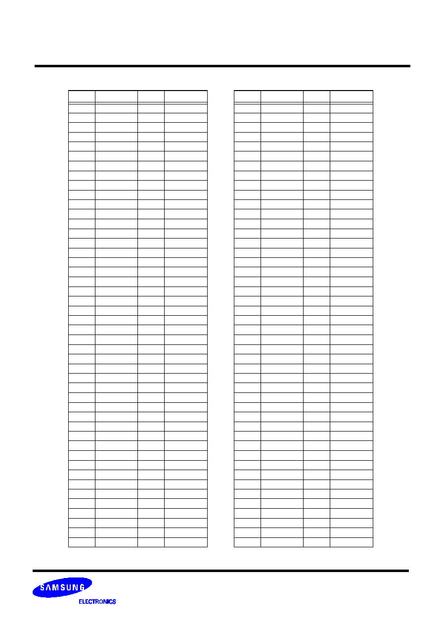
TABLE 2. Module Pad Number and Signal Names
Pin
Pin Name
Pin
Pin Name
Pin
Pin Name
Pin
Pin Name
A1
Gnd
B1
Gnd
A47
NC
B47
NC
A2
LDQA8
B2
LDQA7
A48
NC
B48
NC
A3
Gnd
B3
Gnd
A49
NC
B49
NC
A4
LDQA6
B4
LDQA5
A50
NC
B50
NC
A5
Gnd
B5
Gnd
A51
Vref
B51
Vref
A6
LDQA4
B6
LDQA3
A52
Gnd
B52
Gnd
A7
Gnd
B7
Gnd
A53
SCL
B53
SA0
A8
LDQA2
B8
LDQA1
A54
Vdd
B54
Vdd
A9
Gnd
B9
Gnd
A55
SDA
B55
SA1
A10
LDQA0
B10
LCFM
A56
SVdd
B56
SVdd
A11
Gnd
B11
Gnd
A57
SWP
B57
SA2
A12
LCTMN
B12
LCFMN
A58
Vdd
B58
Vdd
A13
Gnd
B13
Gnd
A59
RSCK
B59
RCMD
A14
LCTM
B14
NC
A60
Gnd
B60
Gnd
A15
Gnd
B15
Gnd
A61
RDQB7
B61
RDQB8
A16
NC
B16
LROW2
A62
Gnd
B62
Gnd
A17
Gnd
B17
Gnd
A63
RDQB5
B63
RDQB6
A18
LROW1
B18
LROW0
A64
Gnd
B64
Gnd
A19
Gnd
B19
Gnd
A65
RDQB3
B65
RDQB4
A20
LCOL4
B20
LCOL3
A66
Gnd
B66
Gnd
A21
Gnd
B21
Gnd
A67
RDQB1
B67
RDQB2
A22
LCOL2
B22
LCOL1
A68
Gnd
B68
Gnd
A23
Gnd
B23
Gnd
A69
RCOL0
B69
RDQB0
A24
LCOL0
B24
LDQB0
A70
Gnd
B70
Gnd
A25
Gnd
B25
Gnd
A71
RCOL2
B71
RCOL1
A26
LDQB1
B26
LDQB2
A72
Gnd
B72
Gnd
A27
Gnd
B27
Gnd
A73
RCOL4
B73
RCOL3
A28
LDQB3
B28
LDQB4
A74
Gnd
B74
Gnd
A29
Gnd
B29
Gnd
A75
RROW1
B75
RROW0
A30
LDQB5
B30
LDQB6
A76
Gnd
B76
Gnd
A31
Gnd
B31
Gnd
A77
NC
B77
RROW2
A32
LDQB7
B32
LDQB8
A78
Gnd
B78
Gnd
A33
Gnd
B33
Gnd
A79
RCTM
B79
NC
A34
LSCK
B34
LCMD
A80
Gnd
B80
Gnd
A35
Vcmos
B35
Vcmos
A81
RCTMN
B81
RCFMN
A36
SOUT
B36
SIN
A82
Gnd
B82
Gnd
A37
Vcmos
B37
Vcmos
A83
RDQA0
B83
RCFM
A38
NC
B38
NC
A84
Gnd
B84
Gnd
A39
Gnd
B39
Gnd
A85
RDQA2
B85
RDQA1
A40
NC
B40
NC
A86
Gnd
B86
Gnd
A41
Vdd
B41
Vdd
A87
RDQA4
B87
RDQA3
A42
Vdd
B42
Vdd
A88
Gnd
B88
Gnd
A43
NC
B43
NC
A89
RDQA6
B89
RDQA5
A44
NC
B44
NC
A90
Gnd
B90
Gnd
A45
NC
B45
NC
A91
RDQA8
B91
RDQA7
A46
NC
B46
NC
A92
Gnd
B92
Gnd

Page 3
Rev.0.9 Apr. 1999
4/6/8/12/16d RIMM
TM
Module with 128Mb RDRAMs
KMMR18R84(6/8/C/G)C
KMMR16R84(6/8/C/G)C
4/6/8/12/16d RIMM
TM
Module with 144Mb RDRAMs
Preliminary
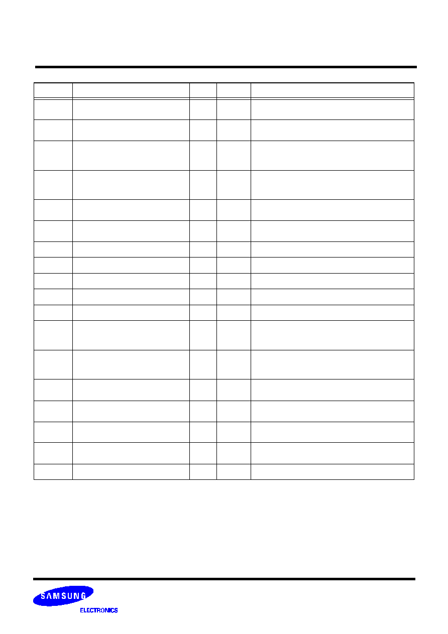
TABLE 3. Module Connector Pad Description
Signal
Pins
I/O
Type
Description
Gnd
A1, A3, A5, A7, A9, A11, A13, A15,
A17, A19, A21, A23, A25, A27, A29,
A31, A33, A39, A52, A60, A62, A64,
A66, A68, A70, A72, A74, A76, A78,
A80, A82, A84, A86, A88, A90, A92,
B1, B3, B5, B7, B9, B11, B13, B15,
B17, B19, B21, B23, B25, B27, B29,
B31, B33, B39, B52, B60, B62, B64,
B66, B68, B70, B72, B74, B76, B78,
B80, B82, B84, B86, B88, B90, B92
Ground reference for RDRAM core and interface. 72
PCB connector pads.
LCFM
B10
I
RSL
Clock from master. Interface clock used for receiving
RSL signals from the Channel. Positive polarity.
LCFMN
B12
I
RSL
Clock from master. Interface clock used for receiving
RSL signals from the Channel. Negative polarity.
LCMD
B34
I
V
CMOS
Serial Command used to read from and write to the con-
trol registers. Also used for power management.
LCOL4..
LCOL0
A20, B20, A22, B22, A24
I
RSL
Column bus. 5-bit bus containing control and address
information for column accesses.
LCTM
A14
I
RSL
Clock to master. Interface clock used for transmitting
RSL signals to the Channel. Positive polarity.
LCTMN
A12
I
RSL
Clock to master. Interface clock used for transmitting
RSL signals to the Channel. Negative polarity.
LDQA8..
LDQA0
A2, B2, A4, B4, A6, B6, A8, B8, A10
I/O
RSL
Data bus A. A 9-bit bus carrying a byte of read or write
data between the Channel and the RDRAM. LDQA8 is
non-functional on modules with x16 RDRAM devices
LDQB8..
LDQB0
B32, A32, B30, A30, B28, A28, B26,
A26, B24
I/O
RSL
Data bus B. A 9-bit bus carrying a byte of read or write
data between the Channel and the RDRAM. LDQB8 is
non-functional on modules with x16 RDRAM devices.
LROW2..
LROW0
B16, A18, B18
I
RSL
Row bus. 3-bit bus containing control and address infor-
mation for row accesses.
LSCK
A34
I
V
CMOS
Serial Clock input. Clock source used to read from and
write to the RDRAM control registers.
NC
A16, B14, A38, B38, A40, B40, A43,
B43, A44, B44, A45, B45, A46, B46,
A47, B47, A48, B48, A49, B49, A50,
B50, A77, B79
These pads are not connected. These 24 connector pads
are reserved for future use.
RCFM
B83
I
RSL
Clock from master. Interface clock used for receiving
RSL signals from the Channel. Positive polarity.
RCFMN
B81
I
RSL
Clock from master. Interface clock used for receiving
RSL signals from the Channel. Negative polarity.
RCMD
B59
I
V
CMOS
Serial Command Input. Pin used to read from and write
to the control registers. Also used for power manage-
ment.
RCOL4..
RCOL0
A73, B73, A71, B71, A69
I
RSL
Column bus. 5-bit bus containing control and address
information for column accesses.
Page 4
4/6/8/12/16d RIMM
TM
Module with 128Mb RDRAMs
KMMR18R84(6/8/C/G)C
KMMR16R84(6/8/C/G)C
4/6/8/12/16d RIMM
TM
Module with 144Mb RDRAMs
Preliminary
Rev.0.9 Apr. 1999
RCTM
A79
I
RSL
Clock to master. Interface clock used for transmitting
RSL signals to the Channel. Positive polarity.
RCTMN
A81
I
RSL
Clock to master. Interface clock used for transmitting
RSL signals to the Channel. Negative polarity.
RDQA8..
RDQA0
A91, B91, A89, B89, A87, B87, A85,
B85, A83
I/O
RSL
Data bus A. A 9-bit bus carrying a byte of read or write
data between the Channel and the RDRAM. RDQA8 is
non-functional on modules x16 RDRAM devices.
RDQB8..
RDQB0
B61, A61, B63, A63, B65, A65, B67,
A67, B69
I/O
RSL
Data bus B. A 9-bit bus carrying a byte of read or write
data between the Channel and the RDRAM. RDQB8 is
non-functional on modules x16 RDRAM devices.
RROW2..
RROW0
B77, A75, B75
I
RSL
Row bus. 3-bit bus containing control and address infor-
mation for row accesses.
RSCK
A59
I
V
CMOS
Serial Clock input. Clock source used to read from and
write to the RDRAM control registers.
SA0
B53
I
SV
DD
Serial Presence Detect Address 0.
SA1
B55
I
SV
DD
Serial Presence Detect Address 1.
SA2
B57
I
SV
DD
Serial Presence Detect Address 2.
SCL
A53
I
SV
DD
Serial Presence Detect Clock.
SDA
A55
I/O
SV
DD
Serial Presence Detect Data (Open Collector I/O).
SIN
B36
I/O
V
CMOS
Serial I/O for reading from and writing to the control
registers. Attaches to SIO0 of the first RDRAM on the
module.
SOUT
A36
I/O
V
CMOS
Serial I/O for reading from and writing to the control
registers. Attaches to SIO1 of the last RDRAM on the
module.
SV
DD
A56, B56
SPD Voltage. Used for signals SCL, SDA, SWE, SA0,
SA1 and SA2.
SWP
A57
I
SV
DD
Serial Presence Detect Write Protect (active high). When
low, the SPD can be written as well as read.
V
CMOS
A35, B35, A37, B37
CMOS I/O Voltage. Used for signals CMD, SCK, SIN,
SOUT.
Vdd
A41, A42, A54, A58, B41, B42, B54,
B58
Supply voltage for the RDRAM core and interface logic.
Vref
A51, B51
Logic threshold reference voltage for RSL signals.
Signal
Pins
I/O
Type
Description
Page 5
4/6/8/12/16d RIMM
TM
Module with 128Mb RDRAMs
KMMR18R84(6/8/C/G)C
KMMR16R84(6/8/C/G)C
4/6/8/12/16d RIMM
TM
Module with 144Mb RDRAMs
Preliminary
Rev.0.9 Apr. 1999
D
Q
A
8
D
Q
A
7
D
Q
A
6
D
Q
A
5
D
Q
A
4
D
Q
A
3
D
Q
A
2
D
Q
A
1
D
Q
A
0
C
F
M
C
F
M
N
C
T
M
C
T
M
N
R
O
W
2
R
O
W
1
R
O
W
0
C
O
L
4
C
O
L
3
C
O
L
2
C
O
L
1
C
O
L
0
D
Q
B
0
D
Q
B
1
D
Q
B
2
D
Q
B
3
D
Q
B
4
D
Q
B
5
D
Q
B
6
D
Q
B
7
D
Q
B
8
SIO0
SIO1
SCK
CMD
Vref
Direct RDRAM (128/144Mb)
R
D
Q
A
8
R
D
Q
A
7
R
D
Q
A
6
R
D
Q
A
5
R
D
Q
A
4
R
D
Q
A
3
R
D
Q
A
2
R
D
Q
A
1
R
D
Q
A
0
R
C
F
M
R
C
F
M
N
R
C
T
M
R
C
T
M
N
R
R
O
W
2
R
R
O
W
1
R
R
O
W
0
R
C
O
L
4
R
C
O
L
3
R
C
O
L
2
R
C
O
L
1
R
C
O
L
0
R
D
Q
B
0
R
D
Q
B
1
R
D
Q
B
2
R
D
Q
B
3
R
D
Q
B
4
R
D
Q
B
5
R
D
Q
B
6
R
D
Q
B
7
R
D
Q
B
8
L
D
Q
A
8
L
D
Q
A
7
L
D
Q
A
6
L
D
Q
A
5
L
D
Q
A
4
L
D
Q
A
3
L
D
Q
A
2
L
D
Q
A
1
L
D
Q
A
0
L
C
F
M
L
C
F
M
N
L
C
T
M
L
C
T
M
N
L
R
O
W
2
L
R
O
W
1
L
R
O
W
0
L
C
O
L
4
L
C
O
L
3
L
C
O
L
2
L
C
O
L
1
L
C
O
L
0
L
D
Q
B
0
L
D
Q
B
1
L
D
Q
B
2
L
D
Q
B
3
L
D
Q
B
4
L
D
Q
B
5
L
D
Q
B
6
L
D
Q
B
7
L
D
Q
B
8
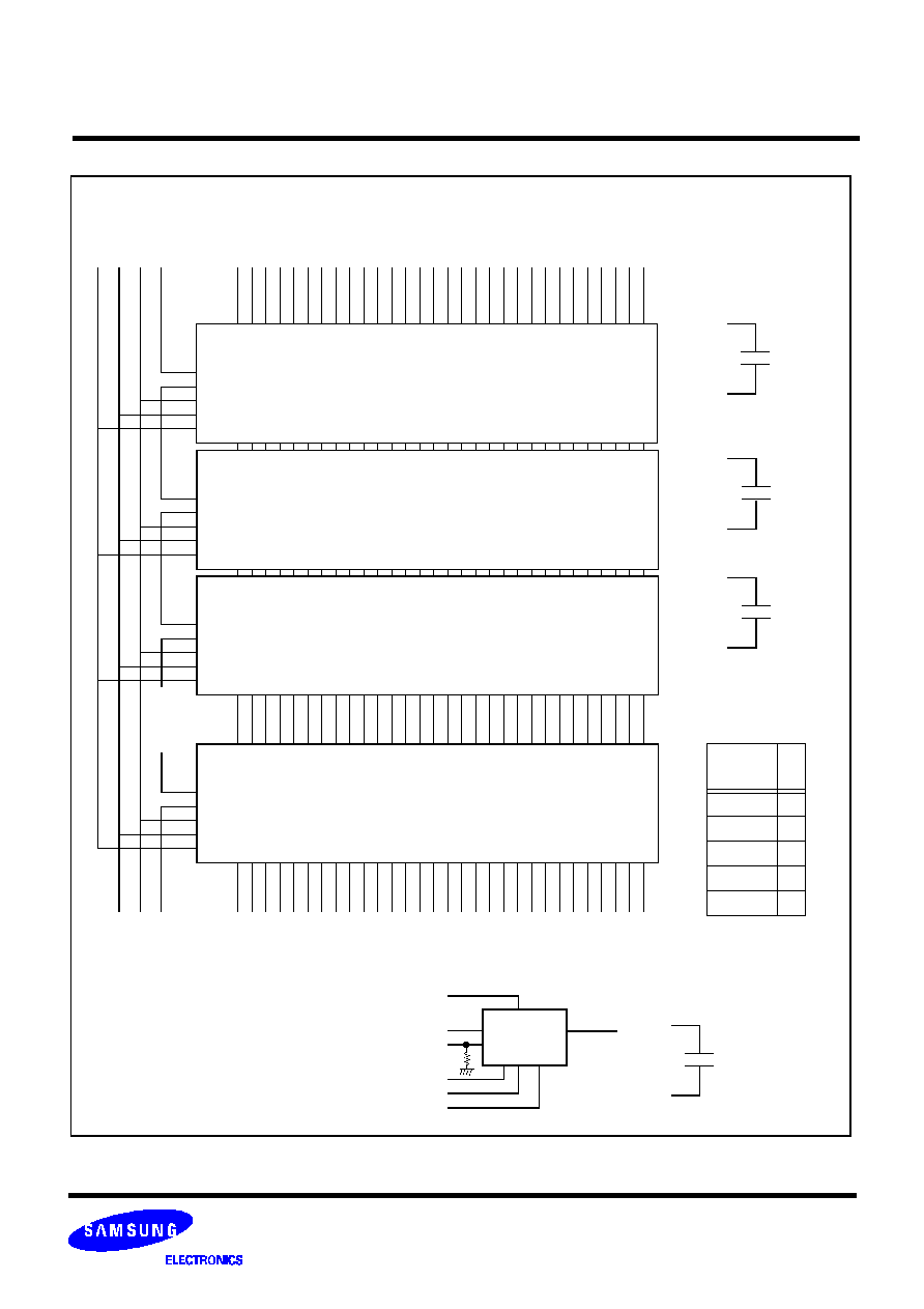
U1
S
I
N
L
S
C
K
L
C
M
D
V
R
E
F
S
O
U
T
R
S
C
K
R
C
M
D
Vdd
Gnd
2 per
RDRAM
SCL
SDA
A0 A1
SCL
SA0
SA1
SDA
Serial Presence Detect
Note 1. Rambus Channel signals form a loop through
the RIMM module, with the exception of the SIO chain.
D
Q
A
8
D
Q
A
7
D
Q
A
6
D
Q
A
5
D
Q
A
4
D
Q
A
3
D
Q
A
2
D
Q
A
1
D
Q
A
0
C
F
M
C
F
M
N
C
T
M
C
T
M
N
R
O
W
2
R
O
W
1
R
O
W
0
C
O
L
4
C
O
L
3
C
O
L
2
C
O
L
1
C
O
L
0
D
Q
B
0
D
Q
B
1
D
Q
B
2
D
Q
B
3
D
Q
B
4
D
Q
B
5
D
Q
B
6
D
Q
B
7
D
Q
B
8
SIO0
SIO1
SCK
CMD
Vref
Direct RDRAM (128/144Mb)
D
Q
A
8
D
Q
A
7
D
Q
A
6
D
Q
A
5
D
Q
A
4
D
Q
A
3
D
Q
A
2
D
Q
A
1
D
Q
A
0
C
F
M
C
F
M
N
C
T
M
C
T
M
N
R
O
W
2
R
O
W
1
R
O
W
0
C
O
L
4
C
O
L
3
C
O
L
2
C
O
L
1
C
O
L
0
D
Q
B
0
D
Q
B
1
D
Q
B
2
D
Q
B
3
D
Q
B
4
D
Q
B
5
D
Q
B
6
D
Q
B
7
D
Q
B
8
SIO0
SIO1
SCK
CMD
Vref
Direct RDRAM (128/144Mb)
D
Q
A
8
D
Q
A
7
D
Q
A
6
D
Q
A
5
D
Q
A
4
D
Q
A
3
D
Q
A
2
D
Q
A
1
D
Q
A
0
C
F
M
C
F
M
N
C
T
M
C
T
M
N
R
O
W
2
R
O
W
1
R
O
W
0
C
O
L
4
C
O
L
3
C
O
L
2
C
O
L
1
C
O
L
0
D
Q
B
0
D
Q
B
1
D
Q
B
2
D
Q
B
3
D
Q
B
4
D
Q
B
5
D
Q
B
6
D
Q
B
7
D
Q
B
8
SIO0
SIO1
SCK
CMD
Vref
Direct RDRAM (128/144Mb)
V
REF
Gnd
1 per
2 RDRAMs
V
CMOS
Gnd
1 per
2 RDRAMs
A2
SA2
WP
SWP
U0
Vcc
SV
DD
0.1
µ
F
0.1
µ
F
0.1
µ
F
SV
DD
Gnd
0.1
µ
F
Plus one
Near Connector
47K
U2
U3
UN
∑
∑
∑
∑
∑
∑
Note 2. See Serial Presence Detection Specification for
information on the SPD device and its contents.
Module
Capacity
N
256MB
16
192MB
12
128MB
8
96MB
6
64MB
4
Figure 2: RIMM Module Functional Diagram
Page 6
Rev.0.9 Apr. 1999
4/6/8/12/16d RIMM
TM
Module with 128Mb RDRAMs
KMMR18R84(6/8/C/G)C
KMMR16R84(6/8/C/G)C
4/6/8/12/16d RIMM
TM
Module with 144Mb RDRAMs
Preliminary
Absolute Maximum Ratings
DC Recommended Electrical Conditions
a. The table below shows the number of 128Mb or 144Mb RDRAM devices contained in a RIMM module of listed memory storage capacity.
Table a. Number of RDRAM devices
Symbol
Parameter
Min
Max
Unit
V
I,ABS
Voltage applied to any RSL or CMOS singnal pad with respect to Gnd
- 0.3
V
DD
+ 0.3
V
V
DD,ABS
Voltage on VDD with respect to Gnd
- 0.5
V
DD
+ 1.0
V
T
STORE
Storage temperature
- 50
100
∞
C
Symbol
Parameter and Conditions
Min
Max
Unit
V
DD
Supply voltage
2.50 - 0.13
2.50 + 0.13
V
V
CMOS
CMOS I/O power supply at pad for 2.5V controllers:
CMOS I/O power supply at pad for 1.8V controllers:
2.5 - 0.13
1.8 - 0.1
2.5 + 0.25
1.8 + 0.2
V
V
V
REF
Reference voltage
1.4 - 0.2
1.4 + 0.2
V
V
IL
RSL input low voltage
V
REF
- 0.5
V
REF
- 0.2
V
V
IH
RSL input high voltage
V
REF
+ 0.2
V
REF
+ 0.5
V
V
IL,CMOS
CMOS input low voltage
- 0.3
0.5V
CMOS
- 0.25
V
V
IH,CMOS
CMOS input high voltage
0.5V
CMOS
+ 0.25
V
CMOS
+ 0.7
V
V
OL,CMOS
CMOS output low voltage @ I
OL,CMOS
= 1mA
0.3
V
V
OH,CMOS
CMOS output high voltage @ I
OH,CMOS
= -0.25mA
V
CMOS
- 0.3
V
I
REF
V
REF
current @ V
REF,MAX
-10 x no. RDRAMs
a
10 x no. RDRAMs
a
mA
I
SCK,CMD
CMOS input leakage current @ (0
V
CMOS
V
DD
)
-10 x no. RDRAMs
a
10 x no. RDRAMs
a
mA
I
SIN,SOUT
CMOS input leakage current @ (0
V
CMOS
V
DD
)
-10.0
10.0
mA
RIMM Module Capacity
256/288MB
192/216MB
128/144MB
96/108MB
64/72MB
Number of 128Mb or 144Mb RDRAM devices
16
12
8
6
4
Page 7
4/6/8/12/16d RIMM
TM
Module with 128Mb RDRAMs
KMMR18R84(6/8/C/G)C
KMMR16R84(6/8/C/G)C
4/6/8/12/16d RIMM
TM
Module with 144Mb RDRAMs
Preliminary
Rev.0.9 Apr. 1999
AC Electrical Specifications
a. Table below lists parameters and specifications for different storage capacity RIMM Modules that use 128Mb or 144Mb RDRAM devices.
b. Average clock delay is defined as the average delay from finger to finger of all RSL clock nets (CTM, CTMN, CFM and CFMN).
AC Electrical Specifications for RIMM Modules
Symbol
Parameter and Conditions
Min
Typ
Max
Unit
Z
Module Impedance
25.2
28
30.8
W
T
PD
Propagation Delay, all RSL signals
-
See
Table
a
ns
DT
PD
Propagation delay variation of RSL signals with respect to an average clock
delay
b
-10
10
ps
DT
PD-CMOS
Propagation delay variation of SCK and CMD signals with respect to an average
clock delay
b
-100
100
ps
V
a
/V
IN
Attenuation Limit
See
Table
a
%
V
XF
/V
IN
Forward crosstalk coefficient (300ps input rise time @ 20%-80%)
See
Table
a
%
V
XB
/V
IN
Backward crosstalk coefficient (300ps input rise time @ 20%-80%)
See
Table
a
%
Symbol
RIMM Module Capacity
256/288MB
192/216MB
128/144MB
96/108MB
64/72MB
Unit
No. of 128/144Mb RDRAMs
16
12
8
6
4
Parameter and Condition for -800 & -
600 RIMM Modules
Max
Max
Max
Max
Max
T
PD
Propagation Delay, all RSL signals -800
2.06
TBD
1.50
TBD
1.25
ns
Propagation Delay, all RSL signals -600
2.10
TBD
1.60
TBD
1.25
ns
V
a
/V
IN
Attenuation Limit -800
25
TBD
16
TBD
12
%
Attenuation Limit -600
21
TBD
10
TBD
8
%
V
XF
/V
IN
Forward crosstalk coefficient (300ps input
rise time @ 20%-80%) -800
8
TBD
4
TBD
2
%
Forward crosstalk coefficient (300ps input
rise time @ 20%-80%) -600
8
TBD
4
TBD
2
%
V
XB
/V
IN
Backward crosstalk coefficient (300ps
input rise time @ 20%-80%) -800
2.5
TBD
2.0
TBD
1.5
%
Backward crosstalk coefficient (300ps
input rise time @ 20%-80%) -600
2.5
TBD
2.0
TBD
1.5
%
R
DC
DC Resistance Limit -800
1.2
TBD
0.8
TBD
0.6
W
DC Resistance Limit -600
1.2
TBD
0.8
TBD
0.6
W

Page 8
4/6/8/12/16d RIMM
TM
Module with 128Mb RDRAMs
KMMR18R84(6/8/C/G)C
KMMR16R84(6/8/C/G)C
4/6/8/12/16d RIMM
TM
Module with 144Mb RDRAMs
Preliminary
Rev.0.9 Apr. 1999
RIMM Module Supply Current Profile
a. Specifications in this table are maximum guidelines. Actual power will depend on individual RDRAM component specifications, memory controller and
usage patterns.
I
DD
RIMM Module Capacity
256/288MB
192/216MB
128/144MB
96/108MB
64/72MB
Unit
No. of 128/144Mb RDRAMs
16
12
8
6
4
RIMM module power condition
@tCYCLE=2.5ns
a
Max
Max
Max
Max
Max
I
DD1
One RDRAM in Read, balance in NAP mode
641
624
606
597
588
mA
I
DD2
One RDRAM in Read, balance in Standby mode,
no commands
2375
1895
1415
1175
935
mA
I
DD3
One RDRAM in Read, balance in Active mode,
no commands
3575
2775
1975
1575
1175
mA
Page 9
Rev.0.9 Apr. 1999
4/6/8/12/16d RIMM
TM
Module with 128Mb RDRAMs
KMMR18R84(6/8/C/G)C
KMMR16R84(6/8/C/G)C
4/6/8/12/16d RIMM
TM
Module with 144Mb RDRAMs
Preliminary
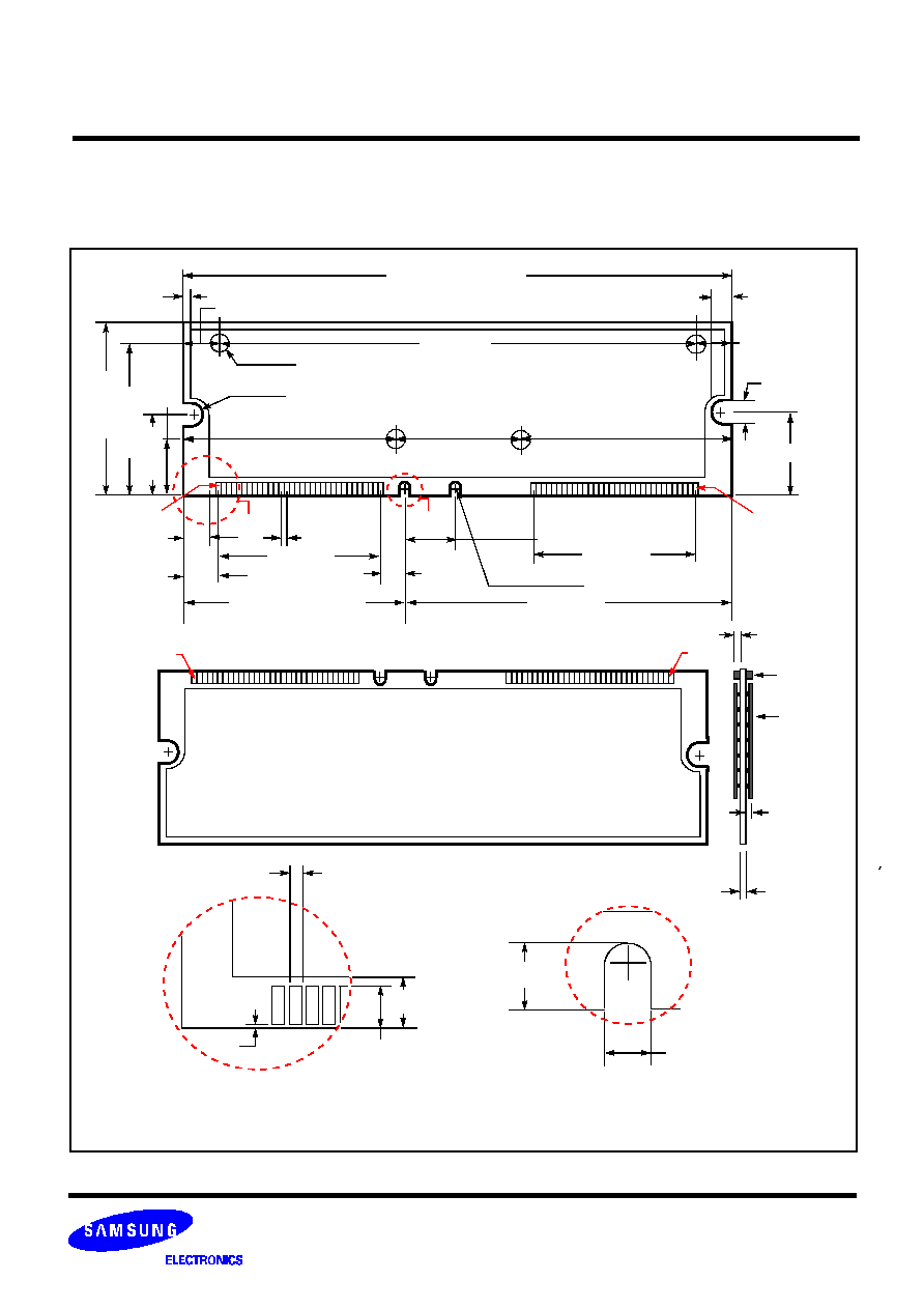
Physical Dimensions
The following defines the RIMM module dimensions. All units are in millimeters with inches in brackets[ ], where appropriate. The
maximum height of the module is 34.93mm[1.375inches].
Figure 3: RIMM Module PCB Physical Dimensions
COMPONENT AREA
(A SIDE)
133.35
±
0.15[5.250
±
0.006]
3.00[0.118]
1.00[0.039]
17.78[0.700]
4.00
±
0.15
45.00[1.772]
1.00[0.039]
4.00[0.157]
5.68[0.2236]
REF.
11.50[0.453]
45.00[1.772]
78.175[3.078]
REF.
55.175
±
0.08[2.172
±
0.003]
DIA 3.18
R 2.00
6.35[0.25]
6.35[0.25]
3
4
.
9
3
[
1
.
3
7
5
]
3
2
.
3
9
[
1
.
2
7
5
]
1
7
.
7
8
[
0
.
7
]
8
.
4
9
[
0
.
3
3
4
]
4.50[0.177]
A-1
A-92
DETAIL A
DETAIL B
120.65[4.75]
(B SIDE)
COMPONENT AREA
B-1
B-92
0.85[0.033]
CAPACITOR
CSP
0.75-1.35
[0.030-0.053]
1.27
±
0.10
[0.050
±
0.004]
0.80
±
0.10
0.15
±
0.10
2.99
±
0.05
[0.031
±
0.004]
[0.006
±
0.004]
[0.12
±
0.002]
DETAIL A
3.00
±
0.10
2.00
±
0.10
DETAIL B
[0.12
±
0.004]
[0.079
±
0.004]
3.99
±
0.10
[0.16
±
0.004]
R 1.00
[0.157
±
0.006]

Page 10
Rev.0.9 Apr. 1999
4/6/8/12/16d RIMM
TM
Module with 128Mb RDRAMs
KMMR18R84(6/8/C/G)C
KMMR16R84(6/8/C/G)C
4/6/8/12/16d RIMM
TM
Module with 144Mb RDRAMs
Preliminary
Table Of Contents
Overview . . . . . . . . . . . . . . . . . . . . . . . . . . . . . . . . . . 1
Features . . . . . . . . . . . . . . . . . . . . . . . . . . . . . . . . . . . 1
Key Timing Parameters/Part Numbers . . . . . . . . . . . 1
Module Pad Numbers and Signal Names . . . . . . . . . 2
Module Connector Pad Description . . . . . . . . . . . . .3-4
RIMM Module Functional Diagram . . . . . . . . . . . . . . 5
Absolute Maximum Ratings . . . . . . . . . . . . . . . . . . . . 6
DC Recommended Electrical Conditions . . . . . . . . . 6
AC Electrical Specifications . . . . . . . . . . . . . . . . . . . . 7
RIMM Module Supply Current Profile . . . . . . . . . . . . 8
Physical Dimensions . . . . . . . . . . . . . . . . . . . . . . . . . 9
© Copyright April 1999 Samsung Electronics.
All rights reserved.
Direct Rambus and Direct RDRAM, SO-RIMM and RIMM
are trademarks of Rambus Inc. Rambus, RDRAM, and the
Rambus Logo are registered trademarks of Rambus Inc.
This document contains advanced information that is subject
to change by Samsung without notice
Document Version 0.9
Samsung Electronics Co., Ltd.
#24 Nongseo-Ri, Kiheung-Eup Yongin-City
Kyunggi-Do, KOREA
Telephone: 82-331-209-4584
Fax: 82-2-760-7990
http://www.samsungsemi.com