 | ÐлекÑÑоннÑй компоненÑ: KS57P0504 | СкаÑаÑÑ:  PDF PDF  ZIP ZIP |
Äîêóìåíòàöèÿ è îïèñàíèÿ www.docs.chipfind.ru

KS57C0502/C0504/P0504 MICROCONTROLLER
PRODUCT OVERVIEW
11
1
PRODUCT OVERVIEW
The KS57C0502/C0504 single-chip CMOS microcontroller has been designed for high-performance using
Samsung's newest 4-bit CPU core, SAM47 (Samsung Arrangeable Microcontrollers).
The KS57P0504 is the microcontroller which has 4 Kbyte one-time-programmable ROM and the functions are
the same to KS57C0502/C0504. With a four-channel comparator, eight LED direct drive pins, serial I/O
interface, and its versatile 8-bit timer/counter, the KS57C0502/C0504 offers an excellent design solution for a
wide variety of general-purpose applications.
Up to 24 pins of the 30-pin SDIP package can be dedicated to I/O. Five vectored interrupts provide fast re-
sponse to internal and external events. In addition, the KS57C0502/C0504's advanced CMOS technology
provides for very low power consumption and a wide operating voltage range -- all at a very low cost.
FEATURES SUMMARY
MEMORY
512
×
4-bit data memory (RAM)
2048
×
8-bit program memory (ROM):KS57C0502
4096
×
8-bit program memory (ROM):KS57C0504
24 I/O PINS
I/O: 18 pins, including 8 high current pins
Input only: 6 pins
COMPARATOR
4-channel mode:
Internal reference (4-bit resolution)
16-step variable reference voltage
3-channel mode:
External reference
150 mV resolution (worst case)
8-BIT BASIC TIMER
Programmable interval timer
Watch-dog timer
8-BIT TIMER/COUNTER
Programmable interval timer
External event counter function
Timer/counter clock output to TCLO0 pin
WATCH TIMER
Time interval generation: 0.5 s, 3.9 ms at 4.19 MHz
4 frequency outputs to BUZ pin
8-BIT SERIAL I/O INTERFACE
8-bit transmit/receive mode
8-bit receive-only mode
LSB-first or MSB-first transmission selectable
Internal or external clock source
BIT SEQUENTIAL CARRIER
Supports 16-bit serial data transfer in arbitrary
format
INTERRUPTS
Two external interrupt vectors
Three internal interrupt vectors
Two quasi-interrupts
MEMORY-MAPPED I/O STRUCTURE
Data memory bank 15
TWO POWER-DOWN MODES
Idle mode: Only CPU clock stops
Stop mode: System clock stops
OSCILLATION SOURCES
Crystal, Ceramic for system clock
Crystal/ceramic: 0.4 - 6.0 MHz
CPU clock divider circuit (by 4. 8, or 64)
INSTRUCTION EXECUTION TIMES
0.95, 1.91, 15.3 µs at 4.19 MHz
0.67, 1.33, 10.7 µs at 6.0 MHz
OPERATING TEMPERATURE
40
°
C to 85
°
C
OPERATING VOLTAGE RANGE
1.8 V to 5.5 V
PACKAGE TYPE
30 SDIP, 32 SOP

PRODUCT OVERVIEW
KS57C0502/C0504/P0504 MICROCONTROLLER
12
FUNCTION OVERVIEW
SAM47 CPU
All KS57-series microcontrollers have the advanced SAM47 CPU core. The SAM47 CPU can directly address
up to 32 K bytes of program memory. The arithmetic logic unit (ALU) performs 4-bit addition, subtraction, logical,
and shift-and-rotate operations in one instruction cycle and most 8-bit arithmetic and logical operations in two
cycles.
CPU REGISTERS
Program Counter
A 11-bit program counter (PC) stores addresses for instruction fetch during program execution. Usually, the
PC is incremented by the number of bytes of the instruction being fetched. An exception is the 1-byte instruction
REF which is used to reference instructions stored in a look-up table in the ROM. Whenever a reset operation or
an interrupt occurs, bits PC11 through PC0 are set to the vector address. Bit PC1312 is reserved to support
future expansion of the device's ROM size.
Stack Pointer
An 8-bit stack pointer (SP) stores addresses for stack operations. The stack area is located in the general-
purpose data memory bank 0. The SP is read or written by 8-bit instructions and SP bit 0 must always be set to
logic zero.
During an interrupt or a subroutine call, the PC value and the PSW are saved to the stack area in RAM. When
the service routine has completed, the values referenced by the stack pointer are restored. Then, the next
instruction is executed.
The stack pointer can access the stack regardless of data memory access enable flag status. Since the reset
value of the stack pointer is not defined in firmware, it is recommended that the stack pointer be initialized to 00H
by program code. This sets the first register of the stack area to data memory location 0FFH.
PROGRAM MEMORY
In its standard configuration, the 4096
×
8-bit ROM is divided into three functional areas:
-- 16-byte area for vector addresses
-- 96-byte instruction reference area
-- 1920-byte general purpose area (KS57C0502)
-- 3968-byte general purpose area (KS57C0504)
The vector address area is used mostly during reset operations and interrupts. These 16 bytes can also be
used as general-purpose ROM.
The REF instruction references 2
×
1-byte and 2-byte instructions stored in locations 0020H007FH. The REF
instruction can also reference three-byte instructions such as JP or CALL. In order for REF to be able to
reference these instructions, however, JP or CALL must be shortened to a 2-byte format. To do this, JP or CALL
is is written to the reference area with the format TJP or TCALL instead of the normal instruction name. Unused
locations in the instruction reference area can be allocated to general-purpose use.

KS57C0502/C0504/P0504 MICROCONTROLLER
PRODUCT OVERVIEW
13
DATA MEMORY
Overview
Data memory is organized into three areas:
-- 32
×
4-bit working registers
-- 224
×
4-bit general-purpose area in bank 0
-- 256
×
4-bit general-purpose area in bank 1
-- 128
×
4-bit area in bank 15 for memory-mapped I/O addresses
Data stored in data memory can be manipulated by 1-, 4-, and 8-bit instructions.
Data memory is organized into two memory banks -- bank 0, bank 1 and bank 15. The select memory bank
instruction (SMB) selects the bank to be used as working data memory. After power-on reset operation,
initialization values for data memory must be redefined by code.
Data Memory Addressing Modes
The enable memory bank (EMB) flag controls the addressing mode for data memory banks 0, 1 or 15.
When the EMB flag is logic zero, restricted area can be accessed. When the EMB flag is set to logic one, all
two data memory banks can be accessed according to the current SMB value. The EMB = "0" addressing mode
is used for normal program execution, whereas the EMB = "1" mode is commonly used for interrupts,
subroutines, mapped I/O, and repetitive access of specific RAM addresses.
Working Registers
The RAM's working register area in data memory bank 0 is further divided into four register banks. Each
register bank has eight 4-bit registers that are addressable either by 1-bit or 4-bit instructions. Paired 4-bit
registers can be addressed as double registers by 8-bit instructions.
Register A is the 4-bit accumulator and double register EA is the 8-bit extended accumulator. Double registers
WX, WL, and HL are used as data pointers for indirect addressing. Unused working registers can be used as
general-purpose memory.
To limit the possibility of data corruption due to incorrect register bank addressing, register bank 0 is usually
used by the main program and banks 1, 2, and 3 for interrupt service routines.
PRODUCT OVERVIEW
KS57C0502/C0504/P0504 MICROCONTROLLER
14
CONTROL REGISTERS
Program Status Word
The 8-bit program status word (PSW) controls ALU operations and instruction execution sequencing. It is also
used to restore a program's execution environment when an interrupt has been serviced. Program instructions
can always address the PSW regardless of the current value of data memory enable flags.
Before an interrupt or subroutine is processed, the PSW is pushed onto the stack in data memory bank 0.
When the service routine is completed, the PSW values are restored.
IS1
IS0
EMB
ERB
C
SC2
SC1
SC0
Interrupt status flags (IS1, IS0), the enable memory bank and enable register bank flags (EMB, ERB), and the
carry flag (C) are 1- and 4-bit read/write or 8-bit read-only addressable. You can address the skip condition flags
(SC0SC2) using 8-bit read instructions only.
Select Bank (SB) Register
Two 4-bit registers store address values used to access specific memory and register banks: the select
memory bank register, SMB, and the select register bank register, SRB.
'SMB n' instruction selects a data memory bank (0 or 15) and stores the upper four bits of the 12-bit data
memory address in the SMB register. To select register bank 0, 1, 2, or 3, and store the address data in the SRB,
you use the instruction 'SRB n'.
The instructions "PUSH SB" and "POP SB" move SRB and SMB values to and from the stack for interrupts
and subroutines.
CLOCK CIRCUITS
System oscillation circuit generates the internal clock signals for the CPU and peripheral hardware.
The system clock can use a crystal, or ceramic oscillation source, or an externally-generated clock signal. To
drive KS57C0502/C0504 using an external clock source, the external clock signal should be input to X
in
, and its
inverted signal to X
out
.
4-bit power control register controls the oscillation on/off, and select the CPU clock. The internal system clock
signal (fx) can be divided internally to produce three CPU clock frequencies -- fx/4, fx/8, or fx/64.
INTERRUPTS
Interrupt requests may be generated internally by on-chip processes (INTB, INTT0, and INTS) or externally by
peripheral devices (INT0 and INT1). There are two quasi-interrupts: INTK and INTW. INTK (KS0KS2) detects
falling edges of incoming signals and INTW detects time intervals of 0.5 seconds or 3.91 milliseconds. The
following components support interrupt processing:
-- Interrupt enable flags
-- Interrupt request flags
-- Interrupt priority registers
-- Power-down termination circuit

KS57C0502/C0504/P0504 MICROCONTROLLER
PRODUCT OVERVIEW
15
POWER-DOWN
To reduce power consumption, there are two power-down modes: idle and stop. The IDLE instruction initiates
idle mode; the STOP instruction initiates stop mode.
In idle mode, the CPU clock stops while peripherals continue to operate normally. In stop mode, system clock
oscillation stops completely, halting all operations except for a few basic peripheral functions. A power-down is
terminated either by a
RESET
or by an interrupt (with exception of the external interrupt INT0).
RESET
When
RESET
is input during normal operation or during power-down mode, a reset operation is initiated and
the CPU enters idle mode. When the standard oscillation stabilization time interval (31.3 ms at 4.19 MHz) has
elapsed, normal CPU operation resumes.
I/O PORTS
The KS57C0502/C0504 has seven I/O ports. Pin addresses for all I/O ports are mapped to locations FF0H
FF6H in bank 15 of the RAM. There are 6 input pins and 18 configurable I/O pins including 8 high current I/O
pins for a total of 24 I/O pins. The contents of I/O port pin latches can be read, written, or tested at the
corresponding address using bit manipulation instructions.
TIMERS and TIMER/COUNTER
The timer function has three main components: an 8-bit basic timer, an 8-bit timer/counter, and a watch timer.
The 8-bit basic timer generates interrupt requests at precise intervals, based on the selected internal clock
frequency.
The programmable 8-bit timer/counter is used for counting events, modifying internal clock frequencies, and
dividing external clock signals. The 8-bit timer/counter generates a clock signal (
SCK
) for the serial I/O interface.
The watch timer consists of an 8-bit watch timer mode register, a clock selector, and a frequency divider
circuit. Its functions include real-time, watch-time measurement, and clock generation for frequency output for
buzzer sound.
SERIAL I/O INTERFACE
The serial I/O interface supports the transmission or reception of 8-bit serial data with an external device. The
serial interface has the following functional components:
-- 8-bit mode register
-- Clock selector circuit
-- 8-bit buffer register
-- 3-bit serial clock counter
The serial I/O circuit can be set to transmit-and-receive, or to receive-only mode. MSB-first or LSB-first
transmission is also selectable.
The serial interface can operate with an internal or an external clock source, or using the clock signal
generated by the 8-bit timer/counter. Transmission frequency can be modified by setting the appropriate bits in
the SIO mode register.

PRODUCT OVERVIEW
KS57C0502/C0504/P0504 MICROCONTROLLER
16
BIT SEQUENTIAL CARRIER
The bit sequential carrier (BSC) is a 16-bit register that can be manipulated using 1-, 4-, and 8-bit instructions.
Using 1-bit indirect addressing, addresses and bit locations can be specified sequentially. In this way,
programs can process 16-bit data by moving the bit location sequentially and then incrementing or decrementing
the value of the L register. BSC data can also be manipulated using direct addressing.
COMPARATOR
The KS57C0502/C0504 contains a 4-channel comparator which can be multiplexed to normal input port.
-- Conversion time: 15.2 µs, 121.6 µs at 4.19 MHz
-- Two operation modes:
Three channels for analog input and one channel for external reference voltage input
Four channels for analog input and internal reference voltage level
-- 16-level internal reference voltage generator
-- 150 mV accuracy for input voltage level difference detection (maximum)
-- Comparator enable and disable
The comparison results are read from the 4-bit CMPREG register after the specified conversion time.
KS57C0502/C0504/P0504 MICROCONTROLLER
PRODUCT OVERVIEW
17
BLOCK DIAGRAM
P3.0 / TCL0
P3.1 / TCLO0
P3.2 / CLO
ARITHMETIC
LOGIC UNIT
INTERRUPT
CONTROL
BLOCK
STACK
POINTER
PROGRAM
COUNTER
PROGRAM
STATUS WORD
I/O PORT 0
P0.0 /
SCK
P0.1 / SO
P0.2 / SI
512 x 4-BIT
DATA
MEMORY
SERIAL I/O
PORT
FLAGS
INSTRUCTION DECODER
CLOCK
RESET
Xin
Xout
INTERNAL
INTERRUPTS
P4.0P4.3
P5.0P5.3
P6.0 / KS0
P6.1 / KS1
P6.2 / KS2
P6.3 / BUZ
COMPARATOR
INPUT
PORT 2
INPUT
PORT 1
P1.0 / INT0
P1.1 / INT1
P2.0 / CIN0
P2.1 / CIN1
P2.2 / CIN2
P2.3 / CIN3
PROGRAM MEMORY
KS57C0502: 2 KBYTE
KS57C0504: 4 KBYTE
8-BIT
TIMER/
COUNTER
I/O PORT 4
I/O PORT 5
I/O PORT 6
I/O PORT 3
BASIC
TIMER
WATCH
TIMER
Figure 11. KS57C0502/C0504 Simplified Block Diagram
PRODUCT OVERVIEW
KS57C0502/C0504/P0504 MICROCONTROLLER
18
PIN ASSIGNMENTS
V
DD
P6.3 / BUZ
P6.2 / KS2
P6.1 / KS1
P6.0 / KS0
P5.3
P5.2
P5.1
P5.0
P4.3
P4.2
P4.1
P4.0
P3.2 / CLO
P3.1 / TCLO0
30
29
28
27
26
25
24
23
22
21
20
19
18
17
16
1
2
3
4
5
6
7
8
9
10
11
12
13
14
15
KS57C0502/0504
(Top View)
V
SS
Xout
Xin
TEST
P1.0 / INT0
P1.1 / INT1
RESET
P0.0 /
SCK
P0.1 / SO
P0.2 / SI
P2.0 / CIN0
P2.1 / CIN1
P2.2 / CIN2
P2.3 / CIN3
P3.0 / TCL0
30-pin SDIP
1
2
3
4
5
6
7
8
9
10
11
12
13
14
15
16
KS57C0502/0504
(Top View)
32
31
30
29
28
27
26
25
24
23
22
21
20
19
18
17
32-pin SOP
V
SS
Xout
Xin
TEST
P1.0 / INT0
P1.1 / INT1
RESET
NC
P0.0 /
SCK
P0.1 / SO
P0.2 / SI
P2.0 / CIN0
P2.1 / CIN1
P2.2 / CIN2
P2.3 / CIN3
P3.0 / TCL0
V
DD
P6.3 / BUZ
P6.2 / KS2
P6.1 / KS1
P6.0 / KS0
P5.3
P5.2
P5.1
P5.0
P4.3
P4.2
P4.1
P4.0
NC
P3.2 / CLO
P3.1 / TCLO0
Figure 12. KS57C0502/C0504 Pin Assignment Diagram
KS57C0502/C0504/P0504 MICROCONTROLLER
PRODUCT OVERVIEW
19
PIN DESCRIPTIONS
Table 12. KS57C0502/C0504 Pin Descriptions
Pin Name
Pin
Type
Description
Number
Share Pin
P0.0
P0.1
P0.2
I/O
3-bit I/O port. 1-bit or 3-bit read/write and test is
possible. Pull-up resistors are assignable to input
pins by software and are automatically disabled for
output pins. Pins are individually configurable as
input or output.
8(9)
9(10)
10(11)
SCK
SO
SI
P1.0
P1.1
I
2-bit input port. 1-bit or 2-bit read and test is possible.
Pull-up resistors are assignable by software.
5(5)
6(6)
INT0
INT1
P2.0P2.3
I
4-bit input port. 1-bit or 4-bit read and test is possible.
11-14
(12-15)
CIN0CIN3
P3.0
P3.1
P3.2
I/O
Same as port 0
15(16)
16(17)
17(18)
TCL0
TCLO0
CLO
P4.0P4.3
P5.0P5.3
I/O
4-bit I/O ports. 1-, 4-, or 8-bit read/write and test is
possible. Pins are individually configurable as input
or output. 4-bit pull-up resistors are software
assignable to input pins and are automatically
disabled for output pins. The N-channel open-drain or
push-pull output can be selected by software (1-bit
unit)
18-21(20-23)
22-25(24-27)
--
P6.0
P6.1
P6.2
P6.3
I/O
4-bit I/O port.
1-bit or 4-bit read/write and test is possible.
Pull-up resistors are assignable to input pins by
software and are automatically disabled for output
pins. Pins are individually configurable as input or
output.
26(28)
27(29)
28(30)
29(31)
KS0
KS1
KS2
BUZ
INT0
I
External interrupts with detection of rising and falling
edges
5(5)
P1.0
INT1
I
External interrupts with detection of rising or falling
edges
6(6)
P1.1
CIN0CIN3
I
4-channel comparator input.
CIN0CIN2: comparator input only.
CIN3: comparator input or external reference input
11-14(12-15)
P2.0P2.3
SCK
I/O
Serial interface clock signal
8(9)
P0.0
SO
I/O
Serial data output
9(10)
P0.1
SI
I/O
Serial data input
10(11)
P0.2
TCL0
I/O
External clock input for timer/counter
15(16)
P3.0
TCLO0
I/O
Timer/counter clock output
16(17)
P3.1
CLO
I/O
CPU clock output
17(18)
P3.2
BUZ
I/O
2 kHz, 4 kHz, 8 kHz, or 16 kHz frequency output at
4.19 MHz for buzzer sound
29(31)
P6.3
NOTE: Pin numbers shown in parentheses '( )' are for 32-pin SOP package; other pin numbers are for the 30-pin SDIP.
PRODUCT OVERVIEW
KS57C0502/C0504/P0504 MICROCONTROLLER
110
Table 12. KS57C0502/C0504 Pin Descriptions (Continued)
Pin Name
Pin
Type
Description
Number
Share Pin
KS0KS2
I/O
Quasi-interrupt input with falling edge detection
26-28(28-30)
P6.0P6.2
V
DD
--
Main power supply
30(32)
--
V
SS
--
Ground
1(1)
--
RESET
I
Reset signal
7(7)
--
TEST
I
Test signal input (must be connected to V
SS
)
4(4)
--
X
in
, X
out
--
Crystal or ceramic oscillator signal for system clock
3,2(3,2)
--
NOTE: Pin numbers shown in parentheses '( )' are for 32-pin SOP package; other pin numbers are for the 30-pin SDIP.
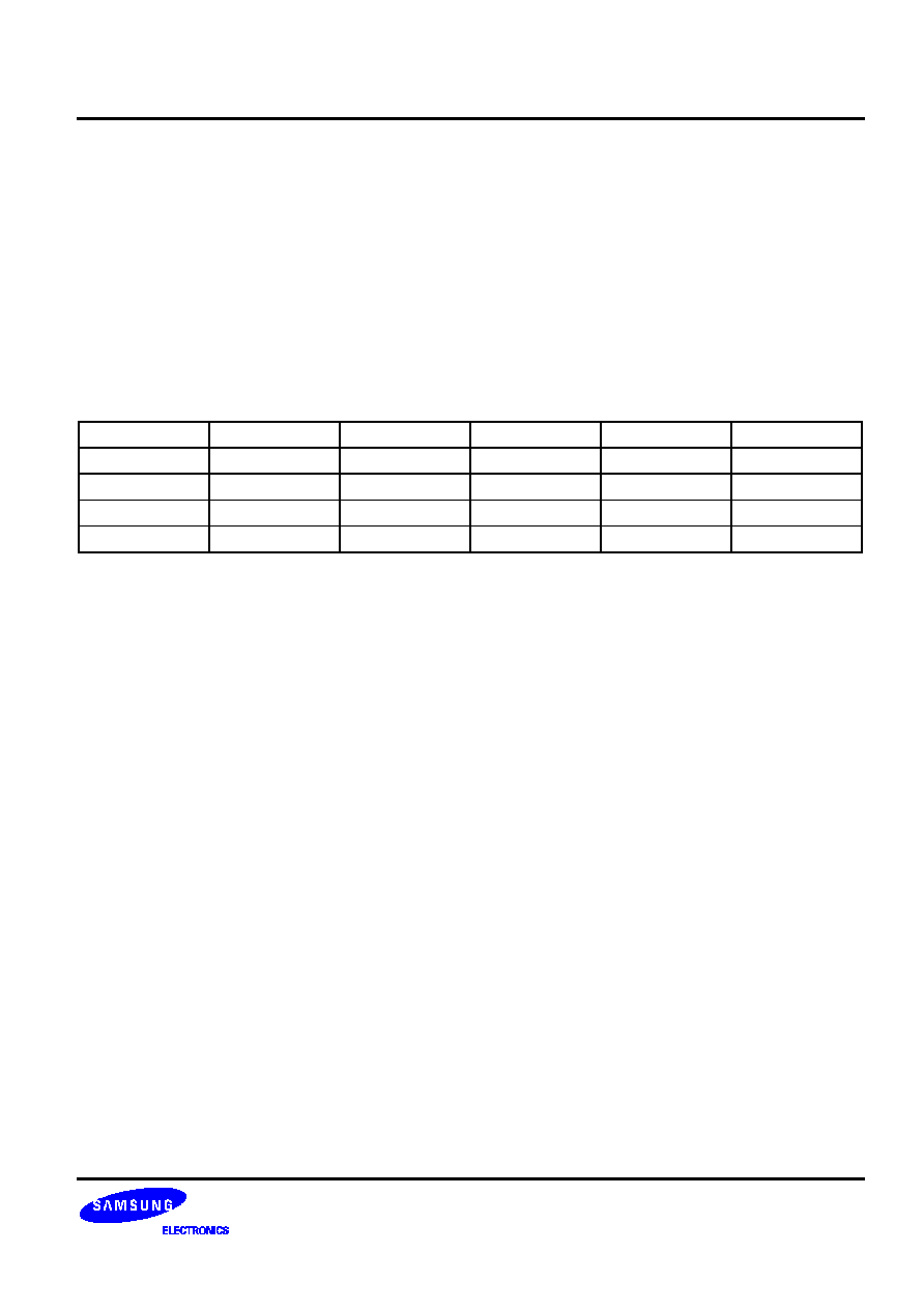
Table 13. Overview of KS57C0502/C0504 Pin Data
SDIP Pin
Numbers
Pin
Names
Share
Pins
I/O
Type
Reset
Value
Circuit
Type
1
V
SS
2,3
Xout, Xin
4
TEST
I
5,6
P1.0, P1.1
INT0, INT1
I
Input
A-3
7
RESET
I
B
8-10
P0.0 - P0.2
SCK
, SO, SI
I/O
Input
D-1
11-14
P2.0 - P2.3
CIN0 - CIN3
I
Input
F-1, F-2
(note)
15-17
P3.0 - P3.2
TCL0, TCLO0,
CLO
I/O
Input
D-1
18-21
P4.0 - P4.3
I/O
Input
E
22-25
P5.0 - P5.3
I/O
Input
E
26-29
P6.0 - P6.3
KS0, KS1, KS2,
BUZ
I/O
Input
D-1
30
V
DD
NOTE: I/O circuit type F-2 is implemented for P2.3 only.
KS57C0502/C0504/P0504 MICROCONTROLLER
PRODUCT OVERVIEW
111
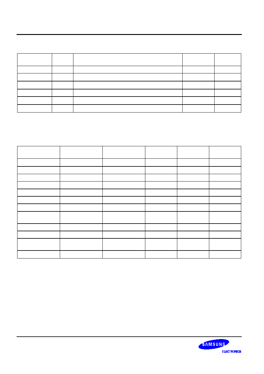
PIN CIRCUIT DIAGRAMS
V
DD
P
-
CHANNEL
IN
N
-
CHANNEL
Figure 13. Pin Circuit Type A
P
-
CHANNEL
RESISTOR
ENABLE
V
DD
PULL-UP
RESISTOR
SCHMITT TRIGGER
IN
Figure 14. Pin Circuit Type A-3
V
DD
PULL-UP
RESISTOR
SCHMITT TRIGGER
IN
Figure 15. Pin Circuit Type B
DATA
OUTPUT
DISABLE
OUT
V
DD
P
-
CHANNEL
N
-
CHANNEL
Figure 16. Pin Circuit Type C
PRODUCT OVERVIEW
KS57C0502/C0504/P0504 MICROCONTROLLER
112
V
DD
PULL-UP
RESISTOR
P
-
CHANNEL
CIRCUIT
TYPE 4
RESISTOR
ENABLE
DATA
OUTPUT
DISABLE
SCHMITT TRIGER
I/O
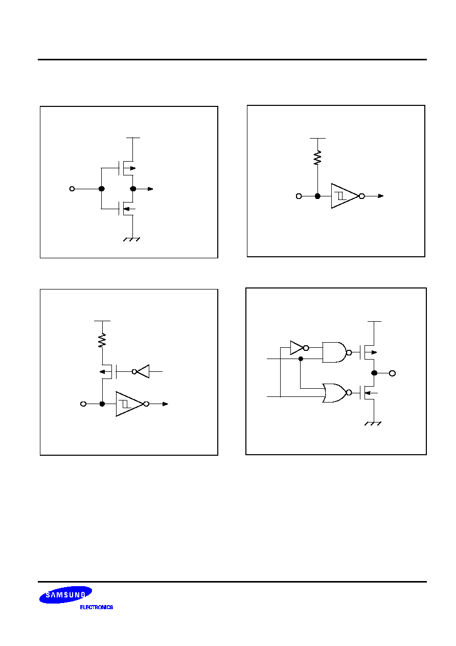
Figure 17. Pin Circuit Type D-1
DATA
OUTPUT
DISABLE
V
DD
P
-
CHANNEL
PULL-UP
RESISTOR
ENABLE
N
-
CHANNEL
PNE
V
DD
PULL-UP
RESISTOR
I/O
Figure 18. Pin Circuit Type E
DIGITAL INPUT
ANALOG INPUT
Figure 19. Pin Circuit Type F-1
DIGITAL INPUT
ANALOG INPUT
EXTERNAL V
REF
Figure 110. Pin Circuit Type F-2

KS57C0502/C0504/P0504 MICROCONTROLLER
ADDRESS SPACES
21
2
ADDRESS SPACES
PROGRAM MEMORY (ROM)
OVERVIEW
ROM maps for KS57C0502/C0504 devices are mask programmable at the factory. In its standard
configuration, the device's 4096
×
8-bit program memory has three areas that are directly addressable by the
program counter (PC):
-- 16-byte area for vector addresses
-- 16-byte general-purpose area
-- 96-byte instruction reference area
-- 1920-byte general-purpose area: KS57C0502
-- 3968-byte general-purpose area: KS57C0504
General-Purpose Memory
Two program memory areas are allocated for general-purpose use: One area is 16 bytes in size and the other
is 1920 bytes (KS57C0502) or 3968 bytes (KS57C0504).
Vector Addresses
You use the 16-byte vector address area to store the vector addresses required to execute
system resets and
interrupts. Start addresses for interrupt service routines are stored in this area, along with the values of the
enable memory bank (EMB) and enable register bank (ERB) flags that are used to set their initial value for the
corresponding service routines. The 16-byte area can be used alternately as general-purpose ROM.
REF Instructions
Locations 0020H007FH are used as a reference area (look-up table) for 1-byte REF instructions. Using REF
instructions, you can reduce the byte size of instruction operands. REF can reference either one 2-byte or two 1-
byte instructions stored in the look-up table. Unused look-up table addresses can be used as general-purpose
ROM.
Table 21. Program Memory Address Ranges
ROM Area Function
Address Ranges
Area Size (in Bytes)
Vector address area
0000H000FH
16
General-purpose program memory
0010H001FH
16
REF instruction look-up table area
0020H007FH
96
General-purpose program memory
0080H07FFH
0080H0FFFH
1920 (KS57C0502)
3968 (KS57C0504)
ADDRESS SPACES
KS57C0502/C0504/P0504 MICROCONTROLLER
22
GENERAL-PURPOSE MEMORY AREAS
The 16-byte area at ROM locations 0010H001FH and the 3968-byte area at ROM locations 0080H0FFFH
are used as general-purpose program memory.
You can also use vacant locations in the vector address area and REF instruction look-up table areas as gen-
eral-purpose program memory. But please be careful not to overwrite live data when writing programs that use
special-purpose areas of the ROM.
VECTOR ADDRESS AREA
Use the 16-byte vector address area of the ROM to store the vector addresses for executing
system resets and
interrupts. The starting addresses of interrupt service routines are stored in this area, along with the enable mem-
ory bank (EMB) and enable register bank (ERB) flag values that are needed to set EMB and ERB's initial values
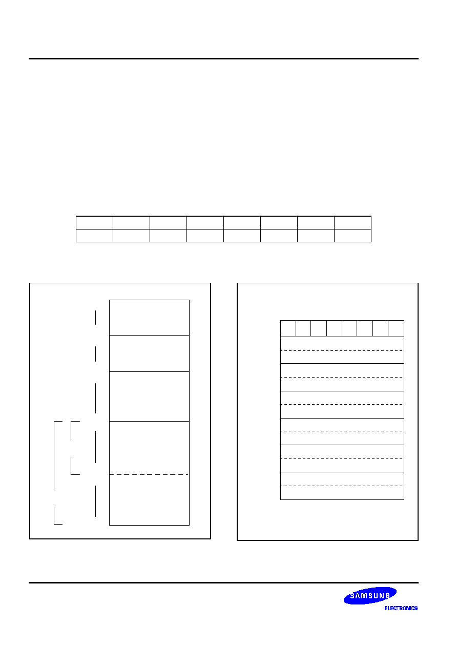
for the service routines. A 16-byte vector address is organized as follows:
EMB
ERB
0
0
PC11
PC10
PC9
PC8
PC7
PC6
PC5
PC4
PC3
PC2
PC1
PC0
To set up the vector address area for specific programs, you use the instruction VENTn. The programming tips
on the next page explain how to do this.
GENERAL-PURPOSE
AREA
(16 Bytes)
GENERAL-PURPOSE
AREA
VECTOR
ADDRESS AREA
(16 Bytes)
INSTRUCTION
REFERENCE AREA
(96 Bytes)
0000H
000FH
0010H
001FH
0020H
007FH
0080H
0FFFH
GENERAL-PURPOSE
AREA
07FFH
0800H
KS57C0502
(1,920 Bytes)
KS57C0504
(3,968 Bytes)
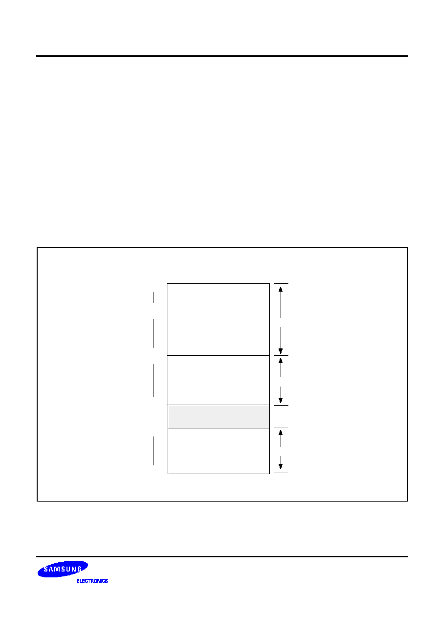
Figure 21. ROM Structure
RESET
INTB
INT0
INT1
INTS
INTT0
0000H
0002H
0004H
0006H
0008H
000AH
7
6
5
4
3
2
1
0
Figure 22. Vector Address Map

KS57C0502/C0504/P0504 MICROCONTROLLER
ADDRESS SPACES
23
+
+
PROGRAMMING TIP -- Defining Vectored Interrupt Areas
The following examples show you several ways you can define the vectored interrupt and instruction reference
areas in program memory:
1.
When all vector interrupts are used:
ORG
0000H
;
VENT0
1,0,RESET
;
EMB
1, ERB
0; Jump to RESET address
VENT1
0,0,INTB
;
EMB
0, ERB
0; Jump to INTB address
VENT2
0,0,INT0
;
EMB
0, ERB
0; Jump to INT0 address
VENT3
0,0,INT1
;
EMB
0, ERB
0; Jump to INT1 address
VENT4
0,0,INTS
;
EMB
0, ERB
0; Jump to INTS address
VENT5
0,0,INTT0
;
EMB
0, ERB
0; Jump to INTT0 address
2.
When a specific vectored interrupt such as INT0, and INTT0 is not used, the unused vector interrupt
locations must be skipped with the assembly instruction ORG so that jumps will address the correct
locations:
ORG
0000H
;
VENT0
1,0,RESET
;
EMB
1, ERB
0; Jump to RESET address
VENT1
0,0,INTB
;
EMB
0, ERB
0; Jump to INTB address
ORG
0006H
;
INT0 interrupt not used
VENT3
0,0,INT1
;
EMB
0, ERB
0; Jump to INT1 address
VENT4
0,0,INTS
;
EMB
0, ERB
0; Jump to INTS address
;
ORG
0010H
;
INTT0 interrupt not used
3.
If an INT0 interrupt is not used and if its corresponding vector interrupt area is not fully utilized, or if it is
not
written by a ORG instruction as in Example 2, a CPU malfunction will occur:
ORG
0000H
;
VENT0
1,0,RESET
;
EMB
1, ERB
0; Jump to RESET address
VENT1
0,0,INTB
;
EMB
0, ERB
0; Jump to INTB address
VENT3
0,0,INT1
;
EMB
0, ERB
0; Jump to INT0 address
VENT4
0,0,INTS
;
EMB
0, ERB
0; Jump to INT1 address
VENT5
0,0,INTT0
;
EMB
0, ERB
0; Jump to INTS address
;
ORG
0010H
;
General-purpose ROM area
;
In this example, when an INTS interrupt is generated, the corresponding vector area is not VENT4 INTS,
but VENT5 INTT0. This causes an INTS interrupt to jump incorrectly to the INTT0 address and causes a
CPU malfunction to occur.

ADDRESS SPACES
KS57C0502/C0504/P0504 MICROCONTROLLER
24
INSTRUCTION REFERENCE AREA
Using 1-byte REF instructions, you can easily reference instructions with larger byte sizes that are stored in
addresses 0020H007FH of program memory. This 96-byte area is called the REF instruction reference area, or
look-up table. Locations in the REF look-up table may contain two one-byte instructions, a single two-byte
instruction, or three-byte instructions such as a JP or CALL. The starting address of the instruction you are
referencing must always be an even number. To reference a JP or CALL instruction, it must be written to the
reference area in a two-byte format: for JP, this format is TJP; for CALL, it is TCALL. In summary, there are
three ways to the REF instruction:
-- Using the 1-byte REF instruction to execute one 2-byte or two 1-byte instructions,
-- Branching to any location by referencing a branch instruction stored in the look-up table,
-- Calling subroutines at any location by referencing a call instruction stored in the look-up table.
+
+
PROGRAMMING TIP -- Using the REF Look-Up Table
Here is one example of how to use the REF instruction look-up table:
ORG
0020H
;
JMAIN
TJP
MAIN
;
0, MAIN
KEYCK
BTSF
KEYFG
;
1, KEYFG CHECK
WATCH
TCALL
CLOCK
;
2, CALL CLOCK
INCHL
LD
@HL,A
;
3, (HL)
A
INCS
HL
·
·
·
ABC
LD
EA,#00H
;
47, EA
#00H
ORG
0080
;
MAIN
NOP
NOP
·
·
·
REF
KEYCK
;
BTSF KEYFG (1-byte instruction)
REF
JMAIN
;
KEYFG = 1, jump to MAIN (1-byte instruction)
REF
WATCH
;
KEYFG = 0, CALL CLOCK (1-byte instruction)
REF
INCHL
;
LD @HL,A
;
INCS HL
REF
ABC
;
LD EA,#00H (1-byte instruction)
·
·
·
KS57C0502/C0504/P0504 MICROCONTROLLER
ADDRESS SPACES
25
DATA MEMORY (RAM)
OVERVIEW
In its standard configuration, the 512
×
4-bit data memory has five areas:
-- 32
×
4-bit working register area
-- 224
×
4-bit general-purpose area in bank 0 (also used as stack area)
-- 256
×
4-bit general-purpose area in bank 1
-- 128
×
4-bit area for memory-mapped I/O addresses
To simplify referencing, the data memory area has two memory banks -- bank 0, bank 1 and bank 15. You
use the select memory bank instruction (SMB) to select the bank you want to use as working data memory. Data
stored in RAM locations are 1-, 4-, and 8-bit addressable. Initialization values for the data memory area are not
defined by hardware and must therefore be initialized by program software following
RESET
. When
RESET
signal
is generated in power-down mode, the data memory contents are maintained.
000H
01FH
020H
0FFH
100H
1FFH
WORKING REGISTERS
(32 x 4 Bits)
GENERAL-PURPOSE
REGISTERS
AND STACK AREA
(224 x 4 Bits)
GENERAL-PURPOSE
(256 x 4 Bits)
F80H
PERIPHRAL
HARDWARE
REGISTERS
FFFH
BANK 0
BANK 1
BANK 15
~
~
~
~
Figure 23. Data Memory (RAM) Map

ADDRESS SPACES
KS57C0502/C0504/P0504 MICROCONTROLLER
26
Memory Banks 0, 1 and 15
Bank 0
(000H0FFH)
The lowest 32 nibbles of bank 0 (000H01FH) are used as working registers;
the next 224
nibbles (020H0FFH) can be used both as stack area and as
general-purpose data memory. Use the stack area for implementing subroutine
calls and returns, and for interrupt processing.
Bank 1
(100H1FFH)
This area is used as general-purpose data memory.
Bank 15
(F80HFFFH)
The microcontroller uses bank 15 for memory-mapped peripheral I/O. Fixed
RAM locations for each peripheral hardware address are mapped into this
area.
Data Memory Addressing Modes
The enable memory bank (EMB) flag controls the addressing mode for data memory banks 0 or 15. When the
EMB flag is logic zero, the addressable area is restricted to specific locations, depending on whether direct or
indirect addressing is used. With direct addressing, you can access locations 000H07FH of bank 0, bank 1 and
bank 15. With indirect addressing, only bank 0 (000H0FFH) can be accessed. When the EMB flag is set to logic
one, all two data memory banks can be accessed according to the current SMB value.
For 8-bit addressing, two 4-bit registers are addressed as a register pair. When using 8-bit instructions to ad-
dress RAM locations, remember to use the even-numbered register address as the instruction operand.
Working Registers
The RAM working register area in data memory bank 0 is further divided into four register banks (bank 0, 1, 2,
and 3). Each register bank has eight 4-bit registers and paired 4-bit registers are 8-bit addressable.
Register A is used as a 4-bit accumulator and register pair EA is an 8-bit extended accumulator. The carry flag
bit can also be used as a 1-bit accumulator. Register pairs WX, WL, and HL are used as address pointers for
indirect addressing. To limit the possibility of data corruption due to incorrect register addressing, it is advisable
to use register bank 0 for the main program and banks 1, 2, and 3 for interrupt service routines.
Bit Sequential Carrier (BSC)
The bit sequential carrier (BSC) is a 16-bit general register mapped to RAM addresses FC0HFC3H that can
be manipulated by 1-, 4-, and 8-bit RAM control instructions.
RESET
clears all bit values to logic zero.
You can specify addresses and bit locations sequentially using a 1-bit indirect addressing instruction. In this
way, a program can process 16-bit data by moving the bit location sequentially, incrementing or decrementing
the value of the L register. BSC data can also be manipulated by direct addressing. For 8-bit manipulations, you
must address the upper and lower 8 bits separately.
KS57C0502/C0504/P0504 MICROCONTROLLER
ADDRESS SPACES
27
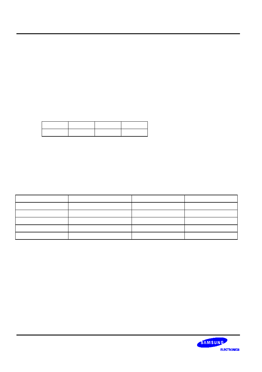
Table 22. Data Memory Organization and Addressing
Addresses
Register Areas
Bank
EMB Value
SMB Value
000H01FH
Working registers
0
0, 1
0
020H0FFH
Stack and general-purpose registers
100H1FFH
General-purpose registers
1
1
1
F80HFFFH
I/O-mapped hardware registers
15
0, 1
15
+
+
PROGRAMMING TIP -- Clearing Data Memory Banks 0 and 1
Clear bank 0 of the data memory area:
RAMCLR
BITS
EMB
SMB
0
LD
HL,#10H
LD
A,#0H
RMCL0
LD
@HL,A
;
RAM (010H0FFH) clear
INCS
HL
JR
RMCL0
;
ADDRESS SPACES
KS57C0502/C0504/P0504 MICROCONTROLLER
28
WORKING REGISTERS
Working registers, mapped to RAM address 000H-01FH in data memory bank 0, are used to temporarily store
intermediate results during program execution, as well as pointer values used for indirect addressing. Unused
registers may be used as general-purpose memory. Working register data can be manipulated as 1-bit units, 4-
bit units or, using paired registers, as 8-bit units.
000H
0001
002H
003H
004H
005H
006H
007H
00FH
010H
017H
018H
01FH
008H
DATA
MEMORY
BANK 0
A ... Y
A
E
L
H
X
W
Z
Y
A
...
Y
WORKING
REGISTER
BANK 0
REGISTER
BANK 1
REGISTER
BANK 2
REGISTER
BANK 3
A
...
Y
A
...
Y
Figure 24. Working Register Map
KS57C0502/C0504/P0504 MICROCONTROLLER
ADDRESS SPACES
29
Working Register Banks
For addressing purposes, the working register area is divided into four register banks -- bank 0, bank 1, bank
2, and bank 3. Any one of these banks can be selected as the working register bank by the register bank
selection instruction (SRBn) and by setting the status of the register bank enable flag (ERB).
Generally, working register bank 0 is used for the main program, and banks 1, 2, and 3 for interrupt service
routines. Following this convention helps to prevent possible data corruption during program execution due to
contention in register bank addressing.
Table 23. Working Register Organization and Addressing
ERB Setting
SRB Settings
Selected Register Bank
3
2
1
0
0
0
0
x
x
Always set to bank 0
0
0
Bank 0
1
0
0
0
1
Bank 1
1
0
Bank 2
1
1
Bank 3
NOTE: 'x' means don't care.
Paired Working Registers
Each of the register banks is subdivided into eight 4-bit registers. These registers are named Y, Z, W, X, H, L,
E and A. You can manipulate them individually using 4-bit instructions, or as register pairs for 8-bit data
manipulation.
The names of the 8-bit register pairs in each register bank are EA, HL, WX, YZ and WL. Registers A, L, X and
Z always become the lower nibble when registers are addressed as 8-bit pairs. This makes a total of eight 4-bit
registers or four 8-bit double registers in each of the four working register banks.
(MSB)
(LSB)
(MSB)
(LSB)
Y
W
H
E
Z
X
L
A
Figure 25. Register Pair Configuration
ADDRESS SPACES
KS57C0502/C0504/P0504 MICROCONTROLLER
210
Special-Purpose Working Registers
You use register A as a 4-bit accumulator and double register EA as an 8-bit accumulator. You can use the
carry flag as a 1-bit accumulator.
8-bit double registers WX, WL and HL are used as data pointers for indirect addressing. When the HL register
serves as a data pointer, the instructions LDI, LDD, XCHI, and XCHD can make very efficient use of working reg-
isters as program loop counters by letting you transfer a value and increment or decrement L register value using
a single instruction.
C
A
EA
8-BIT
ACCUMULATOR
1-BIT
ACCUMULATOR
4-BIT
ACCUMULATOR
Figure 26. 1-Bit, 4-Bit, and 8-Bit Accumulator
Recommendation for Multiple Interrupt Processing
If more than four interrupts are being processed at one time, you can avoid possible loss of working register
data by using the PUSH RR instruction to save register contents to the stack before the service routines are exe-
cuted in the same register bank. When the routines have executed successfully, you can restore the register con-
tents from the stack to working memory using the POP instruction.

KS57C0502/C0504/P0504 MICROCONTROLLER
ADDRESS SPACES
211
+
+
PROGRAMMING TIP -- Selecting Your Working Register Area
The following examples show the correct programming method for selecting working register area:
1.
When ERB = "0":
VENT2
1,0,INT0
;
EMB
1, ERB
0, Jump to INT0 address
;
INT0
PUSH
SB
;
PUSH current SMB, SRB
SRB
2
;
Non-essential instruction, since ERB = "0"
PUSH
HL
;
PUSH HL register to stack
PUSH
WX
;
PUSH WX register to stack
PUSH
YZ
;
PUSH YZ register to stack
PUSH
EA
;
PUSH EA register to stack
SMB
0
LD
EA,#00H
LD
80H,EA
LD
HL,#40H
INCS
HL
LD
WX,EA
LD
YZ,EA
POP
EA
;
POP EA register from stack
POP
YZ
;
POP YZ register from stack
POP
WX
;
POP WX register from stack
POP
HL
;
POP HL register from stack
POP
SB
;
POP current SMB, SRB
IRET
The POP instructions execute alternately with the PUSH instructions. If an SMB ninstruction is used in an
interrupt service routine, a PUSH and POP SB instruction must be used to store and restore the current SMB
and SRB values, as shown in Example 2 below.
2.
When ERB = "1":
VENT2
1,1,INT0
;
EMB
1, ERB
1, Jump to INT0 address
;
INT0
PUSH
SB
;
Store current SMB, SRB
SRB
2
;
Select register bank 2
SMB
0
LD
EA,#00H
LD
80H,EA
LD
HL,#40H
INCS
HL
LD
WX,EA
LD
YZ,EA
POP
SB
;
Restore SMB, SRB
IRET
;
ADDRESS SPACES
KS57C0502/C0504/P0504 MICROCONTROLLER
212
STACK OPERATIONS
STACK POINTER (SP)
The stack pointer (SP) is an 8-bit register that stores the address used to access the stack, an area of data
memory set aside for temporary storage of data and addresses. The SP is mapped to RAM addresses
F80H-F81H, and can be read or written by 8-bit control instructions. When addressing the SP, bit 0 must always
remain cleared to logic zero.
F80H
SP3
SP2
SP1
"0"
F81H
SP7
SP6
SP5
SP4
There are two basic stack operations: writing to the top of the stack (push), and reading from the top of the
stack (pop). A push decrements the SP and a pop increments it so that the SP always points to the top address
of the last data to be written to the stack.
The program counter contents and program status word are stored in the stack area prior to the execution of a
CALL or a PUSH instruction, or during interrupt service routines. Stack operation is a LIFO (Last In-First Out)
type. The stack area is located in general-purpose data memory bank 0.
During an interrupt or a subroutine, the PC value and the PSW are saved to the stack area. When the routine
has completed, the stack pointer is referenced to restore the PC and PSW, and the next instruction is executed.
The SP can address stack registers in bank 0 (addresses 000H-0FFH) regardless of the current value of the
enable memory bank (EMB) flag and the select memory bank (SMB) flag.
Since the reset value of the stack pointer is not defined in firmware, we recommend that you initialize the
stack pointer by program code to location 00H. This sets the first register of the stack area to 0FFH.
NOTE
A subroutine call occupies six nibbles in the stack; an interrupt requires six. When subroutine
nesting or interrupt routines are used continuously, the stack area should be set in accordance with
the maximum number of subroutine levels. To do this, estimate the number of nibbles that will be
used for the subroutines or interrupts and set the stack area correspondingly.
Although you may use general-purpose register areas for stack operations, be careful to avoid data loss due to
simultaneous use of the same register(s).
+
+
PROGRAMMING TIP -- Initializing the Stack Pointer
To initialize the stack pointer (SP):
1.
When EMB = "1":
SMB
15
;
Select memory bank 15
LD
EA,#00H
;
Bit 0 of accumulator A is always cleared to "0"
LD
SP,EA
;
Stack area initial address (0FFH)
(SP) 1
2.
When EMB = "0":
LD
EA,#00H
LD
SP,EA
;
Memory addressing area (00H7FH, F80HFFFH)
KS57C0502/C0504/P0504 MICROCONTROLLER
ADDRESS SPACES
213
PUSH OPERATIONS
Three kinds of push operations reference the stack pointer (SP) to write data from the source register to the
stack: PUSH instructions, CALL instructions, and interrupts. In each case, the SP is decremented by a number
determined by the type of push operation and then points to the next available stack location.
PUSH Instructions
A PUSH instruction references the SP to write two 4-bit data nibbles from the PC to the stack. Two 4-bit stack
addresses are referenced by the stack pointer: one for the upper register value and another for the lower register.
After the PUSH has executed, the SP is decremented by two and points to the next available stack location.
CALL Instructions
When a subroutine call is issued, the CALL instruction references the SP to write the PC's contents to four
4-bit stack locations. Current values for the enable memory bank (EMB) flag and the enable register bank (ERB)
flag are also pushed to the stack. After the CALL has executed, the SP is decremented by six and points to the
next available stack location. Since six 4-bit stack locations are used per CALL, you may nest subroutine calls up
to the number of levels permitted in the stack.
Interrupt Routines
An interrupt routine references the SP to push the contents of the PC, as well as current values for the
program status word (PSW) to the stack. Six 4-bit stack locations are used to store this data. After the interrupt
has executed, the SP is decremented by six and points to the next available stack location. During an interrupt
sequence, subroutines may be nested up to the number of levels which are permitted in the stack area.
SP - 6
SP - 5
SP - 4
SP - 3
SP - 2
SP - 1
SP
SP - 2
SP - 1
SP
SP - 6
SP - 5
SP - 4
SP - 3
SP - 2
SP - 1
SP
CALL
(After CALL, SP SP - 6)
EMB ERB
0
PC3 - PC0
PC7 - PC4
0
0
0
0
0
0
0
0
0
PUSH
(After PUSH, SP SP - 2)
LOWER REGISTER
UPPER REGISTER
(When INT is acknowledged,
SP SP - 6)
INTERRUPT
0
PC3 - PC0
PC7 - PC4
IS1
IS0
EMB ERB
PSW
C
SC2
SC1
SC0
0
0
0
PC 11-PC 8
PC 11-PC 8
Figure 27. Push-Type Stack Operations
ADDRESS SPACES
KS57C0502/C0504/P0504 MICROCONTROLLER
214
POP OPERATIONS
For each push operation there is a corresponding pop operation to write data from the stack back to the source
register or registers: for the PUSH instruction it is the POP instruction; for CALL, the instruction RET or SRET;
for interrupts, the instruction IRET. When a pop operation occurs, the SP is incremented by a number determined
by the type of operation and points to the next free stack location.
POP Instructions
A POP instruction references the SP to write data stored in two 4-bit stack locations back to the register pairs
and SB register. The value for the lower 4-bit register is popped first, followed by the value for the upper 4-bit
register. After the POP has executed, the SP is incremented by two and points to the next free stack location.
RET and SRET Instructions
The end of a subroutine call is signaled by the return instruction, RET or SRET. The RET or SRET uses the
SP to reference the four 4-bit stack locations used for the CALL and to write this data back to the PC, the EMB,
and ERB. After the RET or SRET has executed, the SP is incremented by six and points to the next free stack
location.
IRET Instructions
The end of an interrupt sequence is signaled by the instruction IRET. IRET references the SP to locate the six
4-bit stack addresses used for the interrupt and to write this data back to the PC and the PSW. After the IRET
has executed, the SP is incremented by six and points to the next free stack location.
(SP SP + 2)
POP
LOWER REGISTER
UPPER REGISTER
SP
SP + 1
SP + 2
RET
OR
SRET
(SP
SP + 6)
IRET
(SP SP + 6)
SP
SP + 1
SP + 2
SP + 3
SP + 4
SP + 5
SP + 6
EMB ERB
0
PC3 - PC0
PC7 - PC4
0
0
0
0
0
0
0
0
0
PC11-PC8
SP
SP + 1
SP + 2
SP + 3
SP + 4
SP + 5
SP + 6
0
PC3 - PC0
PC7 - PC4
IS1
IS0
EMB ERB
PSW
C
SC2
SC1 SC0
0
0
0
PC11-PC8
Figure 28. Pop-Type Stack Operations
KS57C0502/C0504/P0504 MICROCONTROLLER
ADDRESS SPACES
215
BIT SEQUENTIAL CARRIER (BSC)
The bit sequential carrier (BSC) is a 16-bit register that is mapped to RAM addresses FC0HFC3H. You can
manipulate the BSC register using 1-, 4-, and 8-bit RAM control instructions.
RESET
clears all BSC bit values to
logic zero.
Using the BSC, you can specify addresses and bit locations sequentially using 1-bit indirect addressing
(memb.@L). Bit addressing is independent of the current EMB value. In this way, programs can process 16-bit
data by moving the bit location sequentially and then incrementing or decrementing the value of the L register.
BSC data can also be manipulated using direct addressing. For 8-bit manipulations, specify the 4-bit register
names BSC0 and BSC2 and manipulate the upper and lower 8 bits manipulated separately.
If the values of the L register are 0H at BSC0.@L, the address and bit location assignment is FC0H.0. If the L
register content is FH at BSC0.@L, the address and bit location assignment is FC3H.3.
Table 24. BSC Register Organization
+
+
PROGRAMMING TIP -- Using the BSC Register to Output 16-Bit Data
To use the bit sequential carrier (BSC) register to output 16-bit data (5937H) to the P3.0 pin:
BITS
EMB
SMB
15
LD
EA,#37H
;
LD
BSC0,EA
;
BSC0
A, BSC1
E
LD
EA,#59H
;
LD
BSC2,EA
;
BSC2
A, BSC3
E
SMB
0
LD
L,#0H
;
AGN
LDB
C,BSC0.@L
;
LDB
P3.0,C
;
P3.0
C
INCS
L
JR
AGN
RET
Name
Address
Bit 3
Bit 2
Bit 1
Bit 0
BSC0
FC0H
BSC0.3
BSC0.2
BSC0.1
BSC0.0
BSC1
FC1H
BSC1.3
BSC1.2
BSC1.1
BSC1.0
BSC2
FC2H
BSC2.3
BSC2.2
BSC2.1
BSC2.0
BSC3
FC3H
BSC3.3
BSC3.2
BSC3.1
BSC3.0
ADDRESS SPACES
KS57C0502/C0504/P0504 MICROCONTROLLER
216
PROGRAM COUNTER (PC)
A 12-bit program counter (PC) stores addresses for instruction fetches during program execution. Whenever a
reset operation
or an interrupt occurs, bits PC11 through PC0 are set to the vector address. Bit PC12PC13 is re-
served to support future expansion of the device's ROM size.
Usually, the PC is incremented by the number of bytes of the instruction being fetched. One exception is the
1-byte REF instruction which is used to reference instructions stored in the ROM.
PROGRAM STATUS WORD (PSW)
The program status word (PSW) is an 8-bit word, mapped to RAM locations FB0HFB1H, that defines system
status and program execution status and which permits an interrupted process to resume operation after an inter-
rupt request has been serviced. PSW values are mapped as follows:
FB0H
IS1
IS0
EMB
ERB
FB1H
C
SC2
SC1
SC0
The PSW can be manipulated by 1-bit or 4-bit read/write and by 8-bit read instructions, depending on the spe-
cific bit or bits being addressed. The PSW can be addressed during program execution regardless of the current
value of the enable memory bank (EMB) flag.
Part or all of the PSW is saved to stack prior to execution of a subroutine call or hardware interrupt. After the
interrupt has been processed, the PSW values are popped from the stack back to the PSW address.
When a
RESET
is generated, the EMB and ERB values are set according to the
RESET
vector address, and
the carry flag is left undefined (or the current value is retained). PSW bits IS0, IS1, SC0, SC1, and SC2 are all
cleared to logic zero.
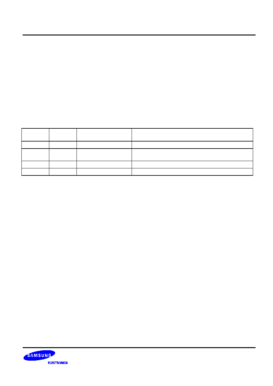
Table 25. Program Status Word Bit Descriptions
PSW Bit Identifier
Description
Bit Addressing
Read/Write
IS1, IS0
Interrupt status flags
1, 4
R/W
EMB
Enable memory bank flag
1
R/W
ERB
Enable register bank flag
1
R/W
C
Carry flag
1
R/W
SC2, SC1, SC0
Program skip flags
8
R
KS57C0502/C0504/P0504 MICROCONTROLLER
ADDRESS SPACES
217
INTERRUPT STATUS FLAGS (IS0, IS1)
PSW bits IS0 and IS1 contain the current interrupt execution status values. They are mapped to RAM bit loca-
tions FB0H.2 and FB0H.3, respectively. You can manipulate IS0 and IS1 flags directly using 1-bit RAM control
instructions
By manipulating interrupt status flags in conjunction with the interrupt priority register (IPR), you can process
multiple interrupts by anticipating the next interrupt in an execution sequence. The interrupt priority control circuit
determines the IS0 and IS1 settings in order to control multiple interrupt processing. When both interrupt status
flags are set to "0", all interrupts are allowed. The priority with which interrupts are processed is then determined
by the IPR.
When an interrupt occurs, IS0 and IS1 are pushed to the stack as part of the PSW and are automatically
incremented to the next higher priority level. Then, when the interrupt service routine ends with an IRET instruc-
tion, IS0 and IS1 values are restored to the PSW. Table 26 shows the effects of IS0 and IS1 flag settings.
Table 26. Interrupt Status Flag Bit Settings
IS1
Value
IS0
Value
Status of Currently
Executing Process
Effect of IS0 and IS1 Settings
on Interrupt Request Control
0
0
0
All interrupt requests are serviced
0
1
1
Only high-priority interrupt(s) as determined in the
interrupt priority register (IPR) are serviced
1
0
2
No more interrupt requests are serviced
1
1
--
Not applicable; these bit settings are undefined
Since interrupt status flags can be addressed by write instructions, programs can exert direct control over
interrupt processing status. Before interrupt status flags can be addressed, however, you must first execute a DI
instruction to inhibit additional interrupt routines. When the bit manipulation has been completed, execute an EI
instruction to re-enable interrupt processing.
+
+
PROGRAMMING TIP -- Setting ISx Flags for Interrupt Processing
The following instruction sequence shows how to use the IS0 and IS1 flags to control interrupt processing:
INTB
DI
; Disable interrupt
BITR IS1
; IS1
0
BITS IS0
; Allow interrupts according to IPR priority level
EI
; Enable interrupt

ADDRESS SPACES
KS57C0502/C0504/P0504 MICROCONTROLLER
218
EMB FLAG (EMB)
The enable memory bank flag EMB is mapped to registers FB0HFB1H in bank 15 of the RAM. The EMB flag
occupies bit location 1 in register FB0H.
The EMB flag is used to allocate specific address locations in the RAM by modifying the upper 4 bits of 12-bit
data memory addresses. In this way, it controls the addressing mode for data memory banks 0, bank 1 or 15.
When the EMB flag is "0", the data memory address space is restricted to bank 15 and addresses 000H07FH
of memory bank 0, regardless of the SMB register contents. When the EMB flag is set to "1", you can access
general-purpose areas of bank 0, bank 1, and bank 15 by using the appropriate SMB value.
+
+
PROGRAMMING TIP -- Using the EMB Flag to Select Memory Banks
EMB flag settings for memory bank selection:
1.
When EMB = "0":
SMB
0
;
Non-essential instruction, since EMB = "0"
LD
90H,A
;
(F90H)
A, bank 15 is selected
LD
34H,A
;
(034H)
A, bank 0 is selected
SMB
15
;
Non-essential instruction, since EMB = "0"
LD
20H,A
;
(020H)
A, bank 0 is selected
LD
90H,A
;
(F90H)
A, bank 15 is selected
;
2.
When EMB = "1":
SMB
0
;
Select memory bank 0
LD
90H,A
;
(090H)
A, bank 0 is selected
LD
34H,A
;
(034H)
A, bank 0 is selected
SMB
15
;
Select memory bank 15
LD
20H,A
;
Program error, but assembler does not detect it
LD
90H,A
;
(F90H)
A, bank 15 is selected
;

KS57C0502/C0504/P0504 MICROCONTROLLER
ADDRESS SPACES
219
ERB FLAG (ERB)
The 1-bit register bank enable flag (ERB) determines the range of addressable working register area. When
the ERB flag is "1", you select the working register area from register banks 0 to 3 according to the register bank
selection register (SRB). When the ERB flag is "0", you select register bank 0 as the working register area,
regardless of the current value of the register bank selection register (SRB).
When an internal
RESET
is generated, bit 6 of program memory address 0000H is written to the ERB flag. This
automatically initializes the flag. When a vectored interrupt is generated, bit 6 of the respective vector address
table in program memory is written to the ERB flag, setting the correct flag status before the interrupt service
routine is executed.
During the interrupt routine, the ERB value is automatically pushed to the stack area along with the other PSW
bits. Afterwards, it is popped back to the FB0H.0 bit location. The initial ERB flag settings for each vectored inter-
rupt are defined using VENTn instructions.
+
+
PROGRAMMING TIP -- Using the ERB Flag to Select Register Banks
ERB flag settings for register bank selection:
1.
When ERB = "0":
SRB
1
;
Register bank 0 is selected (since ERB = "0", the
;
SRB is configured to bank 0)
LD
EA,#34H
;
Bank 0 EA
#34H
LD
HL,EA
;
Bank 0 HL
EA
SRB
2
;
Register bank 0 is selected
LD
YZ,EA
;
Bank 0 YZ
EA
SRB
3
;
Register bank 0 is selected
LD
WX,EA
;
Bank 0 WX
EA
;
2.
When ERB = "1":
SRB
1
;
Register bank 1 is selected
LD
EA,#34H
;
Bank 1 EA
#34H
LD
HL,EA
;
Bank 1 HL
Bank 1 EA
SRB
2
;
Register bank 2 is selected
LD
YZ,EA
;
Bank 2 YZ
BANK 2 EA
SRB
3
;
Register bank 3 is selected
LD
WX,EA
;
Bank 3 WX
Bank 3 EA
;
ADDRESS SPACES
KS57C0502/C0504/P0504 MICROCONTROLLER
220
SKIP CONDITION FLAGS (SC2, SC1, SC0)
The skip condition flags SC2, SC1, and SC0 indicate the current program skip conditions and are set and
reset automatically during program execution. These flags are mapped to RAM bit locations FB1H.0, FB1H.1,
and FB1H.2 of the PSW.
Skip condition flags can only be addressed by 8-bit read instructions. Direct manipulation of the SC2, SC1,
and SC0 bits is not allowed.
CARRY FLAG (C)
The carry flag is mapped to bit location FB1H.3 in the PSW. It is used to save the result of an overflow or
borrow when executing arithmetic instructions involving a carry (ADC, SBC). The carry flag can also be used as
a 1-bit accumulator for performing Boolean operations involving bit-addressed data memory.
If an overflow or borrow condition occurs when executing arithmetic instructions with carry (ADC, SBC), the
carry flag is set to "1". Otherwise, its value is "0". When a
RESET
occurs, the current value of the carry flag is
retained during power-down mode, but when normal operating mode resumes, its value is undefined.
The carry flag can be directly manipulated by predefined set of 1-bit read/write instructions, independent of
other bits in the PSW. Only the ADC and SBC instructions, and the instructions listed in Table 27, affect the
carry flag.
Table 27. Valid Carry Flag Manipulation Instructions
Operation Type
Instructions
Carry Flag Manipulation
Direct manipulation
SCF
Set carry flag to "1"
RCF
Clear carry flag to "0" (reset carry flag)
CCF
Invert carry flag value (complement carry flag)
BTST C
Test carry and skip if C = "1"
Bit transfer
LDB (operand)
(1)
,C
Load carry flag value to the specified bit
LDB C,(operand)
(1)
Load contents of the specified bit to carry flag
Data transfer
RRC A
Rotate right with carry flag
Boolean manipulation
BAND C,(operand)
(1)
AND the specified bit with contents of carry flag and save
the result to the carry flag
BOR C,(operand)
(1)
OR the specified bit with contents of carry flag and save
the result to the carry flag
BXOR C,(operand)
(1)
XOR the specified bit with contents of carry flag and save
the result to the carry flag
Interrupt routine
INTn
(2)
Save carry flag to stack with other PSW bits
Return from interrupt
IRET
Restore carry flag from stack with other PSW bits
NOTES:
1.
The operand has three bit addressing formats: mema.a, memb.@L, and @H + DA.b.
2.
INTn refers to the specific interrupt being executed and is not an instruction.

KS57C0502/C0504/P0504 MICROCONTROLLER
ADDRESS SPACES
221
+
+
PROGRAMMING TIP -- Using the Carry Flag as a 1-Bit Accumulator
1.
Set the carry flag to logic one:
SCF
; C
1
LD
EA,#0C3H
; EA
#0C3H
LD
HL,#0AAH
; HL
#0AAH
ADC
EA,HL
; EA
#0C3H + #0AAH + #1H, C
1
2.
Logical-AND bit 3 of address 3FH with P3.3 and output the result to P5.0:
LD
H,#3H
; Set the upper four bits of the address to the H register value
LDB
C,@H+0FH.3
; C
bit 3 of 3FH
BAND
C,P3.3
; C
C AND P3.3
LDB
P5.0,C
; Output result from carry flag to P5.0

ADDRESS SPACES
KS57C0502/C0504/P0504 MICROCONTROLLER
222
NOTES

KS57C0502/C0504/P0504 MICROCONTROLLER
ADDRESSING MODES
31
3
ADDRESSING MODES
OVERVIEW
The enable memory bank flag, EMB, controls the two addressing modes for data memory. When you enable
the EMB flag, you can address the entire RAM area. When you clear the EMB flag to logic zero, the addressable
RAM is restricted to specific areas.
The EMB flag works in connection with the select memory bank instruction, SMB n. You will recall that the
SMB n instruction is used to select RAM bank 0, bank 1 or 15. The SMB setting is always contained in the upper
four bits of a 12-bit RAM address. For this reason, both addressing modes (EMB = "0" and EMB = "1") apply
specifically to the memory bank indicated by the SMB instruction, and any restrictions to the addressable area
within banks 0, 1 or 15. Direct and indirect 1-bit, 4-bit, and 8-bit addressing methods can be used.
In addition, there are several RAM locations that can always be addressed using specific addressing methods,
regardless of the current EMB flag setting.
Here are a few things to remember about addressing data memory areas:
-- When you address peripheral hardware locations in bank 15, you can use the mnemonic for the memory-
mapped hardware component as the operand in place of the actual address location.
-- Always use an even-numbered RAM address as the operand in 8-bit direct and indirect addressing.
-- With direct addressing, use the RAM address as the instruction operand; with indirect addressing, the
insttruction specifies a register which contains the operand's address.
ADDRESSING MODES
KS57C0502/C0504/P0504 MICROCONTROLLER
32
DA
DA.b
@HL
@H + DA.b
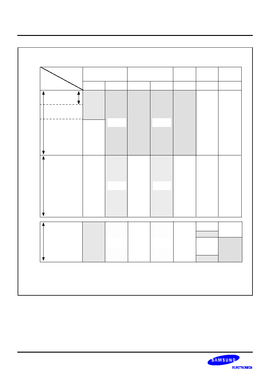
@WX
@WL
mema.b
memb.@L
EMB = 0
EMB = 1
X
X
X
000H
WORKING
REGISTERS
BANK 0
(GENERAL
REGISTERS
AND STACK)
01FH
020H
07FH
080H
0FFH
100H
1FFH
BANK 1:
(GENERAL
REGISTERS)
RAM
AREAS
ADDRESSING
MODE
F80H
FFFH
BANK 15
(PERIPHERAL
HARDWARE
REGISTERS)
FB0H
FBFH
FF0H
FC0H
SMB = 15
SMB = 15
1. 'X' means don't care.
2. Blank columns indicate RAM areas that are not addressable, given the addressing method
and enable memory bank (EMB) flag setting shown in the column headers.
NOTES:
EMB = 1
EMB = 0
SMB = 0
SMB = 0
SMB = 1
SMB = 1
Figure 31. RAM Address Structure

KS57C0502/C0504/P0504 MICROCONTROLLER
ADDRESSING MODES
33
EMB AND ERB INITIALIZATION VALUES
The EMB and ERB flag bits are set automatically by the values of the
RESET
vector address and the interrupt
vector address.
When a
RESET
is generated internally, bit 7 of program memory address 0000H is written to the EMB flag, ini-
tializing it automatically. When a vectored interrupt is generated, bit 7 of the respective vector address table is
written to the EMB. This automatically sets the EMB flag status for the interrupt service routine. When the
interrupt is serviced, the EMB value is automatically saved to stack and then restored when the interrupt routine
has completed.
At the beginning of a program, the initial EMB flag value for each vectored interrupt must be set by using
VENT instruction. The EMB can be set or reset by bit manipulation instructions (BITS, BITR) despite the current
SMB setting.
+
+
PROGRAMMING TIP -- Initializing the EMB and ERB Flags
The following assembly instructions show how to initialize the EMB and ERB flag settings:
ORG
0000H
; ROM address assignment
VENT0
1,0,RESET
; EMB
1, ERB
0, branch RESET
VENT1
0,1,INTB
; EMB
0, ERB
1, branch INTB
VENT2
0,1,INT0
; EMB
0, ERB
1, branch INT0
VENT3
0,1,INT1
; EMB
0, ERB
1, branch INT1
VENT4
0,1,INTS
; EMB
0, ERB
1, branch INTS
VENT5
0,1,INTT0
; EMB
0, ERB
1, branch INTT0
RESET
·
·
·
BITR
EMB
ADDRESSING MODES
KS57C0502/C0504/P0504 MICROCONTROLLER
34
ENABLE MEMORY BANK SETTINGS
EMB = "1"
When you set the enable memory bank flag, EMB, to logic one, you can address the data memory bank
specified by the select memory bank (SMB) value (0,1 or 15) using 1-, 4-, or 8-bit instructions. You can use both
direct and indirect addressing modes. The addressable RAM areas when the EMB flag is set to logic one are as
follows:
If SMB = 0,
000H0FFH
If SMB = 1
100H1FFH
If SMB = 15,
F80HFFFH
EMB = "0"
When the enable memory bank flag EMB is set to logic zero, the addressable area is defined independently of
the SMB value, and is restricted to specific locations depending on whether a direct or indirect address mode is
used.
If EMB = "0", the addressable area is restricted to locations 000H07FH in bank 0 and to locations F80H
FFFH in bank 15 for direct addressing. For indirect addressing, only locations 000H0FFH in bank 0 are
addressable, regardless of SMB value.
To address the peripheral hardware register (bank 15) using indirect addressing, the EMB flag must first be set
to "1" and the SMB value to "15". When a RESET occurs, the EMB flag is set to the value contained in bit 7 of
ROM address 0000H.
EMB-Independent Addressing
You can address several areas of the data memory at any time, despite the status of the EMB flag. These ex-
ceptions are described in Table 31.
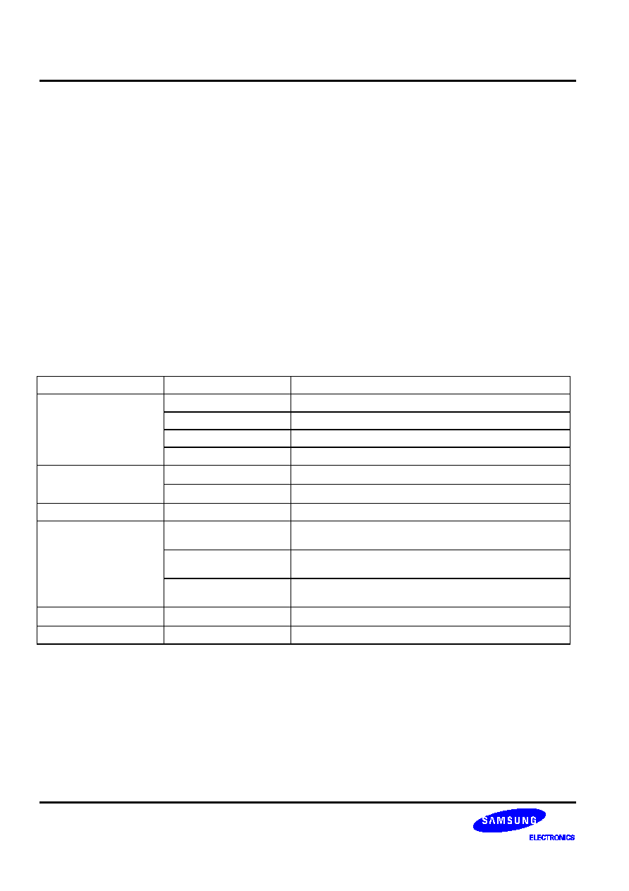
Table 31. RAM Addressing Not Affected by the EMB Value
Address
Addressing Method
Affected Hardware
Program Examples
000H0FFH
4-bit indirect addressing using WX
and WL register pairs;
8-bit indirect addressing using SP
Not applicable
LD A,@WX
PUSH
POP
FB0HFBFH
FF0HFFFH
1-bit direct addressing
PSW,
IEx, IRQx, I/O
BITS EMB
BITR IE1
FC0HFFFH
1-bit indirect addressing using the
L register
BSC,
I/O
BTST FC3H.@L
BAND C,P3.@L
KS57C0502/C0504/P0504 MICROCONTROLLER
ADDRESSING MODES
35
SELECT BANK REGISTER (SB)
The select bank register (SB) is used to assign the memory bank and register bank. The 8-bit SB register con-
sists of the 4-bit select register bank register (SRB) and the 4-bit select memory bank register (SMB), as shown
in Figure 32.
SMB 3 SMB 2 SMB 1 SMB 0
0
0
SRB 1 SRB 0
SRB
SMB
SB
REGISTER
Figure 32. 4-Bit SMB and SRB Values in the SB Register
During interrupts and subroutine calls, SB register contents can be saved to stack in 8-bit units by the PUSH
SB instruction. You later restore the value to the SB using the POP SB instruction.
Select Register Bank (SRB) Instruction
The select register bank (SRB) value specifies which register bank is to be used as a working register bank.
The SRB value is set by the 'SRB n' instruction, where n = 0, 1, 2, 3. One of the four register banks is selected
by the combination of ERB flag status and the SRB value that you set using the 'SRB n' instruction. The current
SRB value is retained until another register is requested by program software.
PUSH SB and POP SB instructions are used to save and restore the contents of SRB during interrupts and
subroutine calls.
RESET
clears the 4-bit SRB value to logic zero.
Select Memory Bank (SMB) Instruction
To select one of the two available data memory banks, you must execute an SMB n instruction specifying the
number of the memory bank you want (0, 1 or 15). For example, the instruction 'SMB 1' selects bank 1 and
'SMB 15' selects bank 15. You must also remember to enable the memory bank you select by the appropriate
enable memory bank flag (EMB) setting.
The upper four bits of the 12-bit data memory address are stored in the SMB register. If the SMB value is not
specified by software (or if a
RESET
does not occur) the current value is retained.
RESET
clears the 4-bit SMB
value to logic zero.
PUSH SB and POP SB instructions save and restore the contents of the SMB register to and from the stack
area during interrupts and subroutine calls.

ADDRESSING MODES
KS57C0502/C0504/P0504 MICROCONTROLLER
36
DIRECT AND INDIRECT ADDRESSING
You can directly address 1-bit, 4-bit, and 8-bit data stored in data memory locations using a specific register or
bit address as the instruction operand.
In indirect addressing the instruction specifies a specfic register pair which contain the address of the operand.
The KS57 instruction set supports 1-bit, 4-bit, and 8-bit indirect addressing. For 8-bit indirect addressing, an
even-numbered RAM address must always be used as the instruction operand, and the address register can be
HL, WX, or WL of the selected register bank.
1-BIT ADDRESSING
Table 32. 1-Bit Direct and Indirect RAM Addressing
Instruction
Notation
Addressing Mode
Description
EMB
Flag
Setting
Addressable
Area
Memory
Bank
Hardware I/O
Mapping
000H07FH
Bank 0
--
DA.b
Direct: bit is indicated by the
RAM address (DA), memory
bank selection, and specified
bit number (b).
0
F80HFFFH
Bank15
All 1-bit
addressable
peripherals
(SMB = 15)
1
000HFFFH
SMB = 0, 1, 15
mema.b
Direct: bit is indicated by ad-
dressable area (mema) and
bit number (b).
x
FB0HFBFH
FF0HFFFH
Bank 15
IS0, IS1, EMB,
ERB, IEx, IRQx,
Pn.n
memb.@L
Indirect: lower two bits of reg-
ister L as indicated by the up-
per 10 bits of RAM area
(memb) and the upper two
bits of register L.
x
FC0HFFFH
Bank 15
BSCn.x
Pn.n
@H + DA.b
Indirect: bit indicated by the
lower four bits of the address
(DA), memory bank selection,
and the H register identifier.
0
000H0FFH
Bank 0
--
1
000HFFFH
SMB = 0, 1, 15
All 1-bit
addressable
peripherals
(SMB = 15)
NOTE
:
'x' means don't care.

KS57C0502/C0504/P0504 MICROCONTROLLER
ADDRESSING MODES
37
+
+
PROGRAMMING TIP -- 1-Bit Addressing Modes
1-Bit Direct Addressing
1.
If EMB = "0":
AFLAG
EQU
34H.3
BFLAG
EQU
85H.3
CFLAG
EQU
0BAH.0
SMB
0
;
Non-essential instruction, since EMB = "0"
BITS
AFLAG
;
34H.3
1
BITS
BFLAG
;
F85H.3 (BMOD.3)
1
BTST
CFLAG
;
If FBAH.0 (IRQW) = 1, skip
BITS
BFLAG
;
Else if FBAH.0 (IRQW) = 0, F85H.3 (BMOD.3)
1
BITS
P3.0
;
FF3H.0 (P3.0)
1
;
2.
If EMB = "1":
AFLAG
EQU
34H.3
BFLAG
EQU
85H.3
CFLAG
EQU
0BAH.0
SMB
0
;
Select memory bank 0
BITS
AFLAG
;
34H.3
1
BITS
BFLAG
;
85H.3
1
BTST
CFLAG
;
If 0BAH.0 = 1, skip
BITS
BFLAG
;
Else if 0BAH.0 = 0, 085H.3
1
BITS
P3.0
;
FF3H.0 (P3.0)
1
;

ADDRESSING MODES
KS57C0502/C0504/P0504 MICROCONTROLLER
38
+
+
PROGRAMMING TIP -- 1-Bit Addressing Modes (Continued)
1-Bit Indirect Addressing
1.
If EMB = "0":
AFLAG
EQU
34H.3
BFLAG
EQU
85H.3
CFLAG
EQU
0BAH.0
SMB
0
;
Non-essential instruction, since EMB = "0"
LD
H,#0BH
;
H
#0BH
BTSTZ
@H+CFLAG
;
If 0BAH.0 = 1, 0BAH.0
0 and skip
BITS
CFLAG
;
Else if 0BAH.0
=
0, FBAH.0 (IRQW)
1
;
2.
If EMB = "1":
AFLAG
EQU
34H.3
BFLAG
EQU
85H.3
CFLAG
EQU
0BAH.0
SMB
0
;
Select memory bank 0
LD
H,#0BH
;
H
#0BH
BTSTZ
@H+CFLAG
;
If 0BAH.0 = 1, 0BAH.0
0 and skip
BITS
CFLAG
;
Else if 0BAH.0
=
0, 0BAH.0
1
;
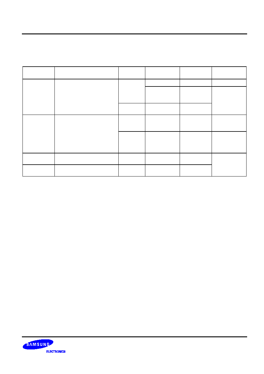
KS57C0502/C0504/P0504 MICROCONTROLLER
ADDRESSING MODES
39
4-BIT ADDRESSING
Table 33. 4-Bit Direct and Indirect RAM Addressing
Instruction
Notation
Addressing Mode
Description
EMB Flag
Setting
Addressable
Area
Memory
Bank
Hardware I/O
Mapping
000H07FH
Bank 0
--
DA
Direct: 4-bit address indicated
by the RAM address (DA) and
the memory bank selection
0
F80HFFFH
Bank15
All 4-bit
addressable
peripherals
1
000HFFFH
SMB = 0,
1,15
(SMB = 15)
@HL
Direct: 4-bit address indicated
by the memory bank selection
and register HL
0
000H0FFH
Bank 0
--
1
000HFFFH
SMB = 0, 15
All 4-bit
addressable
peripherals
(SMB = 15)
@WX
Indirect: 4-bit address indi-
cated by register WX
x
000H0FFH
Bank 0
--
@WL
Indirect: 4-bit address indi-
cated by register WL
x
000H0FFH
Bank 0
NOTE
:
'x' means don't care.
+
+
PROGRAMMING TIP -- 4-Bit Addressing Modes
4-Bit Direct Addressing
1.
If EMB = "0":
ADATA
EQU
46H
BDATA
EQU
8EH
SMB
15
;
Non-essential instruction, since EMB = "0"
LD
A,P3
;
A
(P3)
SMB
0
;
Non-essential instruction, since EMB = "0"
LD
ADATA,A
;
(046H)
A
LD
BDATA,A
;
(F8EH)
A
;
2.
If EMB = "1":
ADATA
EQU
46H
BDATA
EQU
8EH
SMB
15
;
Select memory bank 15
LD
A,P3
;
A
(P3)
SMB
0
;
Select memory bank 0
LD
ADATA,A
;
(046H)
A
LD
BDATA,A
;
(08EH)
A
;

ADDRESSING MODES
KS57C0502/C0504/P0504 MICROCONTROLLER
310
+
+
PROGRAMMING TIP -- 4-Bit Addressing Modes (Continued)
4-Bit Indirect Addressing
1.
If EMB = "0", compare bank 0, locations 040H046H with 060H066H:
ADATA
EQU
46H
BDATA
EQU
66H
SMB
15
;
Non-essential instruction, since EMB = "0"
LD
HL,#BDATA
LD
WX,#ADATA
COMP
LD
A,@WL
;
A
bank 0 (040H046H)
CPSE
A,@HL
;
If bank 0 (060H066H) = A, skip
SRET
DECS
L
JR
COMP
RET
;
2.
If EMB = "1", exchange bank 0, 040H046H with 060H066H:
ADATA
EQU
46H
BDATA
EQU
66H
SMB
0
;
Select memory bank 0
LD
HL,#BDATA
LD
WX,#ADATA
TRANS
LD
A,@WL
;
A
bank 0 (040H046H)
XCHD
A,@HL
;
Bank 0 (060H066H)
A
JR
TRANS
;
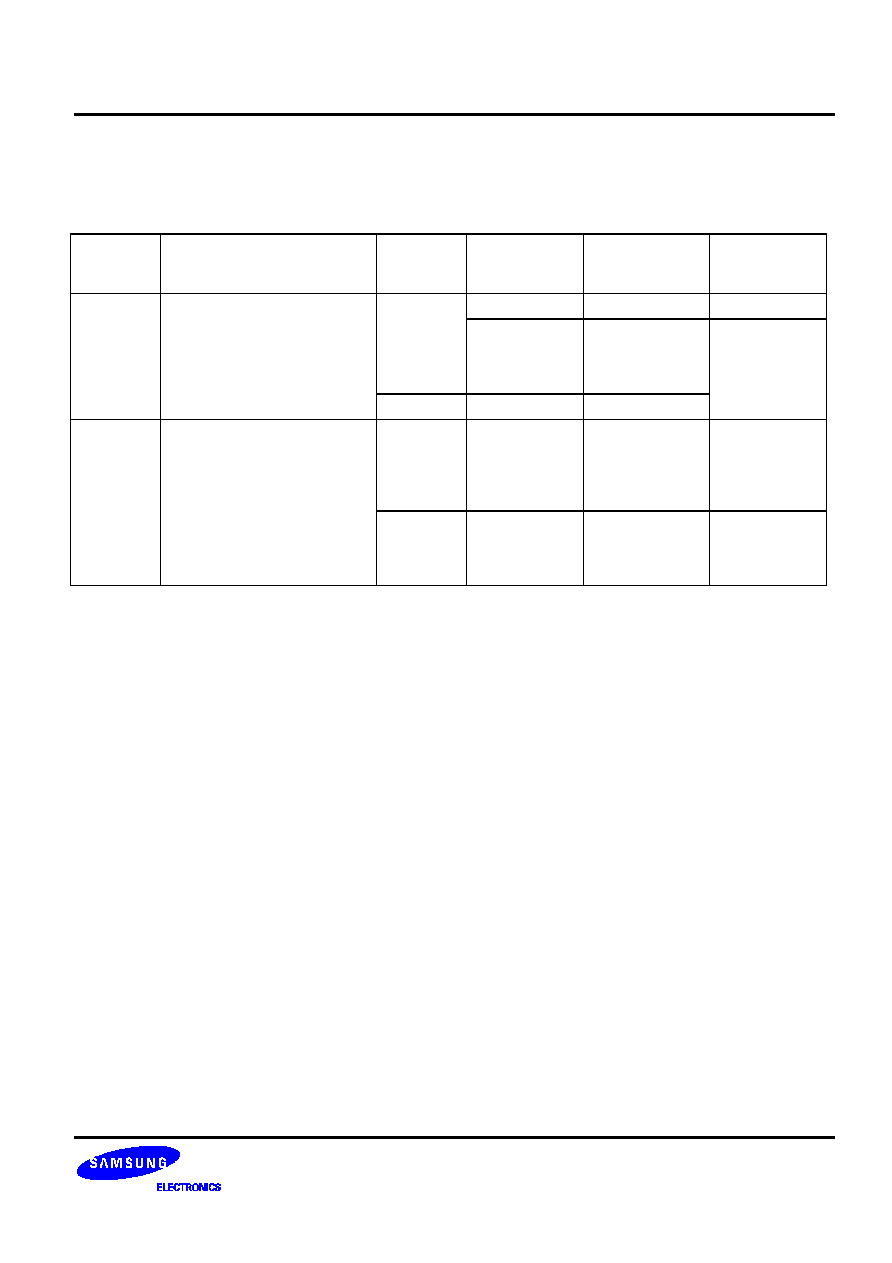
KS57C0502/C0504/P0504 MICROCONTROLLER
ADDRESSING MODES
311
8-BIT ADDRESSING
Table 34. 8-Bit Direct and Indirect RAM Addressing
Instructio
n
Notation
Addressing Mode
Description
EMB Flag
Setting
Addressable
Area
Memory
Bank
Hardware I/O
Mapping
000H07FH
Bank 0
--
DA
Direct: 8-bit address indicated
by the RAM address (DA =
even number) and memory
bank selection
0
F80HFFFH
Bank15
All 8-bit
addressable
peripherals
(SMB = 15)
1
000HFFFH
SMB = 0, 1, 15
@HL
Indirect: the 8-bit address indi-
cated by the memory bank
selection and register HL; (the
4-bit L register value must be
an even number)
0
000H0FFH
Bank 0
--
1
000HFFFH
SMB = 0, 1, 15
All 8-bit
addressable
peripherals
(SMB = 15)
+
+
PROGRAMMING TIP -- 8-Bit Addressing Modes
8-Bit Direct Addressing:
1.
If EMB = "0":
ADATA
EQU
46H
BDATA
EQU
8EH
SMB
15
;
Non-essential instruction, since EMB = "0"
LD
EA,P4
;
E
(P5), A
(P4)
LD
ADATA,EA
;
(046H)
A, (047H)
E
LD
BDATA,EA
;
(F8EH)
A, (F8FH)
E
;
2.
If EMB = "1":
ADATA
EQU
46H
BDATA
EQU
8EH
SMB
15
;
Select memory bank 15
LD
EA,P4
;
E
(P5), A
(P4)
SMB
0
;
Select memory bank 0
LD
ADATA,EA
;
(046H)
A, (047H)
E
LD
BDATA,EA
;
(08EH)
A, (08FH)
E
;

ADDRESSING MODES
KS57C0502/C0504/P0504 MICROCONTROLLER
312
+
+
PROGRAMMING TIP -- 8-Bit Addressing Modes (Continued)
8-Bit Indirect Addressing
1.
If EMB = "0":
ADATA
EQU
8EH
LD
HL,#ADATA
LD
EA,@HL
;
A
(08EH), E
(08FH)
;
2.
If EMB = "1":
ADATA
EQU
46H
SMB
0
LD
HL,#ADATA
LD
EA,@HL
;
A
(046H), E
(047H)
;

KS57C0502/C0504/P0504 MICROCONTROLLER
MEMORY MAP
41
4
MEMORY MAP
OVERVIEW
To support program control of peripheral hardware, I/O addresses for peripherals are memory-mapped to bank
15 of the RAM. Memory mapping lets you use a mnemonic as the operand of an instruction in place of the
specific memory location.
Access to bank 15 is controlled by the select memory bank (SMB) instruction and by the enable memory bank
flag (EMB) setting.If the EMB flag is "0", bank 15 can be addressed using direct addressing, regardless of the
current SMB value. You can use 1-bit direct and indirect addressing, however, for specific locations in bank 15,
regardless of the current EMB value.
I/O MAP FOR HARDWARE REGISTERS
Table 41 contains detailed information about I/O mapping for peripheral hardware in bank 15 (register loca-
tions F80HFFFH). Use the I/O map as a quick-reference source when writing application programs. The I/O
map gives you the following information:
-- Register address
-- Register name (mnemonic for program addressing)
-- Bit values (both addressable and non-manipulable)
-- Read-only, write-only, or read and write addressability
-- 1-bit, 4-bit, or 8-bit data manipulation characteristics
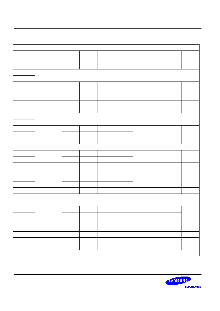
MEMORY MAP
KS57C0502/C0504/P0504 MICROCONTROLLER
42
Table 41. I/O Map for Memory Bank 15
Memory Bank 15
Addressing Mode
Address
Register
Bit 3
Bit 2
Bit 1
Bit 0
R/W
1-Bit
4-Bit
8-Bit
F80H
SP
.3
.2
.1
"0"
R/W
No
No
Yes
F81H
.7
.6
.5
.4
·
·
F85H
BMOD
.3
.2
.1
.0
W
.3
Yes
No
F86H
BCNT
R
No
No
Yes
F87H
F88H
WMOD
"0"
.2
.1
"0"
(1)
W
No
No
Yes
F89H
.7
"0"
.5
.4
·
·
F90H
TMOD0
.3
.2
"0"
"0"
W
.3
No
Yes
F91H
"0"
.6
.5
.4
F92H
"0"
TOE0
"0"
"0"
R/W
Yes
Yes
No
F93H
F94H
TCNT0
R
No
No
Yes
F95H
F96H
TREF0
W
No
No
Yes
F97H
F98H
WDMOD
.3
.2
.1
.0
W
No
No
Yes
F99H
.7
.6
.5
.4
F9AH
WDTCF
.3
"0"
"0"
"0"
W
Yes
No
No
·
·
FB0H
PSW
IS1
IS0
EMB
ERB
R/W
Yes
Yes
Yes
FB1H
C
(2)
SC2
SC1
SC0
R
No
No
FB2H
IPR
IME
.2
.1
.0
W
IME
Yes
No
FB3H
PCON
.3
.2
.1
.0
W
No
Yes
No
FB4H
IMOD0
.3
"0"
.1
.0
W
No
Yes
No
FB5H
IMOD1
"0"
"0"
"0"
.0
W
No
Yes
No
FB6H
IMODK
"0"
.2
.1
.0
W
N o
Yes
No
FB7H
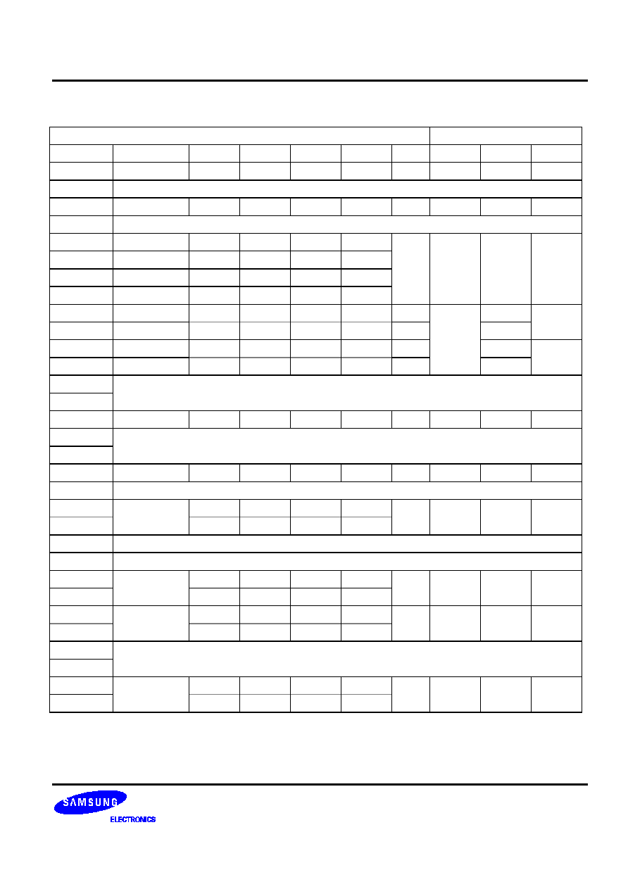
KS57C0502/C0504/P0504 MICROCONTROLLER
MEMORY MAP
43
Table 41. I/O Map for Memory Bank 15 (Continued)
Memory Bank 15
Addressing Mode
Address
Register
Bit 3
Bit 2
Bit 1
Bit 0
R/W
1-Bit
4-Bit
8-Bit
FB8H
"0"
"0"
IEB
IRQB
R/W
Yes
Yes
No
FB9H
FBAH
"0"
"0"
IEW
IRQW
R/W
Yes
Yes
No
FBBH
FBCH
"0"
"0"
IET0
IRQT0
FBDH
"0"
"0"
IES
IRQS
R/W
Yes
Yes
No
FBEH
IE1
IRQ1
IE0
IRQ0
FBFH
"0"
"0"
IEK
IRQK
FC0H
BSC0
R/W
Yes
Yes
Yes
FC1H
BSC1
R/W
Yes
FC2H
BSC2
R/W
Yes
Yes
FC3H
BSC3
R/W
Yes
·
·
FD0H
CLMOD
.3
"0"
.1
.0
W
No
Yes
No
·
·
FD4H
CMPREG
R
No
Yes
No
FD5H
FD6H
CMOD
.3
.2
.1
.0
R/W
No
No
Yes
FD7H
.7
.6
.5
"0"
·
·
FDAH
PNE
PNE4.3
PNE4.2
PNE4.1
PNE4.0
W
No
No
Yes
FDBH
PNE5.3
PNE5.2
PNE5.1
PNE5.0
FDCH
PUMOD
.3
"0"
.1
.0
W
No
No
Yes
FDDH
"0"
.6
.5
.4
FDEH
FDFH
FE0H
SMOD
.3
.2
.1
.0
W
.3
No
Yes
FE1H
.7
.6
.5
"0"
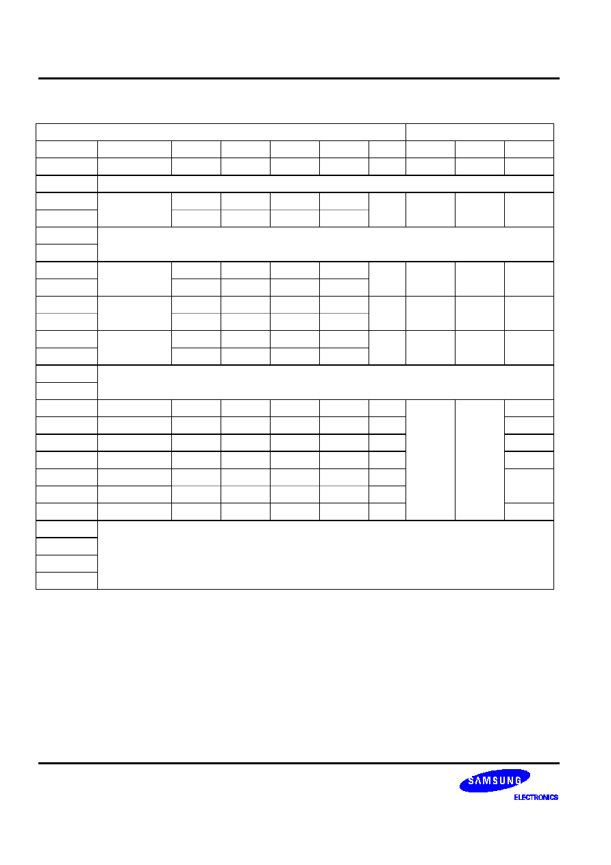
MEMORY MAP
KS57C0502/C0504/P0504 MICROCONTROLLER
44
Table 41. I/O Map for Memory Bank 15 (Concluded)
Memory Bank 15
Addressing Mode
Address
Register
Bit 3
Bit 2
Bit 1
Bit 0
R/W
1-Bit
4-Bit
8-Bit
FE2H
P2MOD
.3
.2
.1
.0
W
No
Yes
No
FE3H
FE4H
SBUF
R/W
No
No
Yes
FE5H
FE6H
FE7H
FE8H
PMG1
"0"
PM0.2
PM0.1
PM0.0
W
No
No
Yes
FE9H
"0"
PM3.2
PM3.1
PM3.0
FEAH
PMG2
PM4.3
PM4.2
PM4.1
PM4.0
W
No
No
Yes
FEBH
"0"
"0"
"0"
"0"
FECH
PMG3
PM5.3
PM5.2
PM5.1
PM5.0
W
No
No
Yes
FEDH
PM6.3
PM6.2
PM6.1
PM6.0
FEEH
FEFH
FF0H
Port 0
--
.2
.1
.0
R/W
Yes
Yes
No
FF1H
Port 1
--
--
.1
.0
R
No
FF2H
Port 2
.3
.2
.1
.0
R
No
FF3H
Port 3
--
.2
.1
.0
R/W
No
FF4H
Port 4
.3
.2
.1
.0
R/W
Yes
FF5H
Port 5
.3 / .7
.2 / .6
.1 / .5
.0 / .4
R/W
FF6H
Port 6
.3
.2
.1
.0
R/W
No
·
·
·
FFFH
NOTES:
1.
Bit 0 in the WMOD register must be set to logic "0".
2.
The carry flag can be read or written by specific bit manipulation instructions only.

KS57C0502/C0504/P0504 MICROCONTROLLER
MEMORY MAP
45
REGISTER DESCRIPTIONS
In this section, register descriptions are presented in a consistent format to familiarize you with the memory-
mapped I/O locations in bank 15 of the RAM. Figure 41 describes features of the register description format.
Register descriptions are arranged in alphabetical order.
Counter registers, buffer registers, and reference registers, as well as the stack pointer and port I/O latches,
are not included in these descriptions.
This section can be used as a quick-reference source when writing application programs.
More detailed information about each of these registers is included in Part II of this manual, "Hardware
Descriptions," in the context of the corresponding peripheral hardware module descriptions.
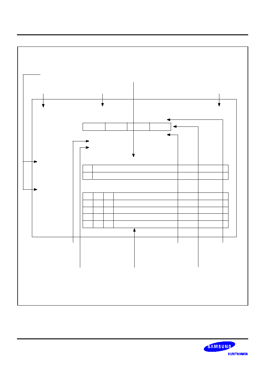
MEMORY MAP
KS57C0502/C0504/P0504 MICROCONTROLLER
46
IPR -- Interrupt Priority Register
FB2H
Bit
Identifier
RESET
Value
Read/Write
Bit Addressing
IME
.2 .0
Global Interrupt Enable Bit
Interrupt Priority Assignment Bits
W
W
W
W
1/4
0
0
0
0
3
2
1
0
IME
.2
.1
.0
0
1
Disable interrupt processing globally
Enable interrupt processing globally
Process I NTB interrupts only
Process INT0 interrupts only
Process INT1 interrupts only
Process INTT interrupts only
Register ID
Register name
Register location
in RAM bank 15
Bit number in
MSB to LSB order
Bit identifier used
for bit addressing
Bit value immediately
following a reset
Type of addressing
that must be used to
address the bit
(1-bit, 4-bit, or 8-bit)
R
W
R/W
''
=
=
=
=
Read-only
Write-only
Read/write
Not used
Bit identifiers used
for bit addressing
Description of the
effect of specific bit
settings
Name of individual
bit or related bits
4
4
4
0
0
0
1
1
Process all interrupt requests at low priority
0
1
0
1
0
0
1
0
1
1
Figure 41. Register Description Format
KS57C0502/C0504/P0504 MICROCONTROLLER
MEMORY MAP
47
BMOD
-- Basic Timer Mode Register
F85H
Bit
3
2
1
0
Identifier
.3
.2
.1
.0
RESET
Value
0
0
0
0
Read/Write
W
W
W
W
Bit Addressing
1/4
4
4
4
BMOD.3
Basic Timer Restart Bit
1
Restart basic timer, then clear IRQB flag, BCNT and BMOD.3 to logic zero
BMOD.2 .0
Input Clock Frequency and Signal Stabilization Interval Control Bits
0
0
0
Input clock frequency:
Signal stabilization interval:
fx / 2
12
(1.02 kHz)
2
20
/ fx (250 ms)
0
1
1
Input clock frequency:
Signal stabilization interval:
fx / 2
9
(8.18 kHz)
2
17
/ fx (31.3 ms)
1
0
1
Input clock frequency:
Signal stabilization interval:
fx / 2
7
(32.7 kHz)
2
15
/ fx (7.82 ms)
1
1
1
Input clock frequency:
Signal stabilization interval:
fx / 2
5
(131 kHz)
2
13
/ fx (1.95 ms)
NOTES:
1.
Signal stabilization interval is the time required to stabilize clock signal oscillation after stop mode is terminated by
an interrupt.
2.
When a
RESET
occurs, the oscillation stabilization time is 31.3 ms at 4.19 MHz.
3.
'fx' is the system clock rate given a clock frequency of 4.19 MHz.
MEMORY MAP
KS57C0502/C0504/P0504 MICROCONTROLLER
48
CMOD
-- Comparator Mode Register
FD7H, FD6H
Bit
7
6
5
4
3
2
1
0
Identifier
.7
.6
.5
"0"
.3
.2
.1
.0
RESET
Value
0
0
0
0
0
0
0
0
Read/Write
R/W
R/W
R/W
R/W
R/W
R/W
R/W
R/W
Bit Addressing
8
8
8
8
8
8
8
8
CMOD.7
Comparator Enable/Disable Bit
1
Comparator operation enable
0
Comparator operation disable
CMOD.5
External/Internal Reference Selection Bit
1
External reference at CIN3, CIN02: analog input
0
Internal reference, CIN03: analog input
CMOD.6
Conversion Time Control Bit
1
4
×
2
4
/ fx, 15.2 µs @4.19 MHz
0
4
×
2
7
/ fx, 121.6 µs @4.19 MHz
CMOD.4
Bit 4
0
Always logic zero
CMOD.3 .0
Reference Voltage Selection Bits
Selected V
REF
V
DD
×
(n + 0.5)
16
, n = 0 to 15
KS57C0502/C0504/P0504 MICROCONTROLLER
MEMORY MAP
49
CLMOD
-- Clock Output Mode Register
FD0H
Bit
3
2
1
0
Identifier
.3
"0"
.1
.0
RESET
Value
0
0
0
0
Read/Write
W
W
W
W
Bit Addressing
4
4
4
4
CLMOD.3
Enable/Disable Clock Output Control Bit
0
Disable clock output
1
Enable clock output
CLMOD.2
Bit 2
0
Always logic zero
CLMOD.1 .0
Clock Source and Frequency Selection Control Bits
0
0
Select CPU clock source fx/4, fx/8, or fx/64 (1.05 MHz, 524 kHz, or 65.6
kHz)
0
1
Select system clock fx/8 (524 kHz)
1
0
Select system clock fx/16 (262 kHz)
1
1
Select system clock fx/64 (65.5 kHz)
NOTE: fx' is the system clock given a clock frequency of 4.19 MHz.
MEMORY MAP
KS57C0502/C0504/P0504 MICROCONTROLLER
410
IE0, 1, IRQ0, 1
-- INT0, 1 Interrupt Enable/Request Flags
FBEH
Bit
3
2
1
0
Identifier
IE1
IRQ1
IE0
IRQ0
RESET
Value
0
0
0
0
Read/Write
R/W
R/W
R/W
R/W
Bit Addressing
1/4
1/4
1/4
1/4
IE1
INT1 Interrupt Enable Flag
0
Disable interrupt requests at the INT1 pin
1
Enable interrupt requests at the INT1 pin
IRQ1
INT1 Interrupt Request Flag
Generate INT1 interrupt (bit is set and cleared by hardware when rising or
falling edge detected at INT1 pin.)
IE0
INT0 Interrupt Enable Flag
0
Disable interrupt requests at the INT0 pin
1
Enable interrupt requests at the INT0 pin
IRQ0
INT0 Interrupt Request Flag
Generate INT0 interrupt (bit is set and cleared by hardware when rising or
falling edge detected at INT0 pin.)
KS57C0502/C0504/P0504 MICROCONTROLLER
MEMORY MAP
411
IEK, IRQK
-- Key Interrupt Enable/Request Register
FBFH
Bit
3
2
1
0
Identifier
0
0
IEK
IRQK
RESET
Value
0
0
0
0
Read/Write
R/W
R/W
R/W
R/W
Bit Addressing
1/4
1/4
1/4
1/4
.3 .2
Bits 32
0
Always logic zero
IEK
Key Interrupt Request Enable Flag
0
Disable INTK interrupt requests at the KS0KS2 pins
1
Enable INTK interrupt requests at the KS0KS2 pin
IRQK
Key Interrupt Request Flag
Generate INTK interrupt. (This bit is set when falling edge detected any at one
of the KS0KS2 pins. INTK is a quasi-interrupt and IRQK must be cleared by
software.)
MEMORY MAP
KS57C0502/C0504/P0504 MICROCONTROLLER
412
IEB, IRQB
-- INTB Interrupt Enable/Request Flags
FB8H
Bit
3
2
1
0
Identifier
0
0
IEB
IRQB
RESET
Value
0
0
0
0
Read/Write
R/W
R/W
R/W
R/W
Bit Addressing
1/4
1/4
1/4
1/4
.3 .2
Bits 32
0
Always logic zero
IEB
INTB Interrupt Enable Flag
0
Disable INTB interrupt requests
1
Enable INTB interrupt requests
IRQB
INTB Interrupt Request Flag
Generate INTB interrupt (bit is set and cleared automatically by hardware when
reference interval signal received from basic timer.)
KS57C0502/C0504/P0504 MICROCONTROLLER
MEMORY MAP
413
IES, IRQS
-- INTS Interrupt Enable/Request Flags
FBDH
Bit
3
2
1
0
Identifier
0
0
IES
IRQS
RESET
Value
0
0
0
0
Read/Write
R/W
R/W
R/W
R/W
Bit Addressing
1/4
1/4
1/4
1/4
.3 .2
Bits 32
0
Always logic zero
IES
INTS Interrupt Enable Flag
0
Disable INTS interrupt requests
1
Enable INTS interrupt requests
IRQS
INTS Interrupt Request Flag
Generate INTS interrupt (bit is set and cleared automatically by hardware when
transmit or receive operation is completed.)
MEMORY MAP
KS57C0502/C0504/P0504 MICROCONTROLLER
414
IET0, IRQT0
-- INTT0 Interrupt Enable/Request Flags
FBCH
Bit
3
2
1
0
Identifier
0
0
IET0
IRQT0
RESET
Value
0
0
0
0
Read/Write
R/W
R/W
R/W
R/W
Bit Addressing
1/4
1/4
1/4
1/4
.3 .2
Bits 32
0
Always logic zero
IET0
INTT0 Interrupt Enable Flag
0
Disable INTT0 interrupt requests
1
Enable INTT0 interrupt requests
IRQT0
INTT0 Interrupt Request Flag
Generate INTT0 interrupt (bit is set and cleared automatically by hardware
when contents of TCNT0 and TREF0 registers match.)
KS57C0502/C0504/P0504 MICROCONTROLLER
MEMORY MAP
415
IEW, IRQW
-- INTW Interrupt Enable/Request Flags
FBAH
Bit
3
2
1
0
Identifier
0
0
IEW
IRQW
RESET
Value
0
0
0
0
Read/Write
R/W
R/W
R/W
R/W
Bit Addressing
1/4
1/4
1/4
1/4
.3 .2
Bits 32
0
Always logic zero
IEW
INTW Interrupt Enable Flag
0
Disable INTW interrupt requests
1
Enable INTW interrupt requests
IRQW
INTW Interrupt Request Flag
Generate INTW interrupt (bit is set when timer interval = 0.5 s or 3.19 ms)
NOTE: INTW is a quasi-interrupt and its request flag must be cleared by software.
MEMORY MAP
KS57C0502/C0504/P0504 MICROCONTROLLER
416
IMOD0
-- External Interrupt 0 (INT0) Mode Register
FB4H
Bit
3
2
1
0
Identifier
.3
"0"
.1
.0
RESET
Value
0
0
0
0
Read/Write
W
W
W
W
Bit Addressing
4
4
4
4
IMOD0.3
Interrupt Sampling Clock Selection Bit
0
Select CPU clock as a sampling clock
1
Select sampling clock frequency of the system clock (fx)/64
IMOD0.2
Bit 2
0
Always logic zero
IMOD0.1 .0
External Interrupt Mode Control Bits
0
0
Interrupt requests are triggered by a rising signal edge
0
1
Interrupt requests are triggered by a falling signal edge
1
0
Interrupt requests are triggered by both rising and falling signal edges
1
1
Interrupt request flag (IRQ0) cannot be set to logic one
KS57C0502/C0504/P0504 MICROCONTROLLER
MEMORY MAP
417
IMOD1
-- External Interrupt 1 (INT1) Mode Register
FB5H
Bit
3
2
1
0
Identifier
"0"
"0"
"0"
.0
RESET
Value
0
0
0
0
Read/Write
W
W
W
W
Bit Addressing
4
4
4
4
IMOD1.3 .1
Bits 31
0
Always logic zero
IMOD1.0
External Interrupt 1 Edge Detection Control Bit
0
Rising edge detection
1
Falling edge detection
MEMORY MAP
KS57C0502/C0504/P0504 MICROCONTROLLER
418
IMODK
-- Key Interrupt Mode Register
FB6H
Bit
3
2
1
0
Identifier
"0"
.2
.1
.0
RESET
Value
0
0
0
0
Read/Write
W
W
W
W
Bit Addressing
4
4
4
4
IMODK.3
Bits 3
0
Always logic zero
IMODK.2 .0
Key Interrupt Edge Detection Selection Bit
0
0
0
Interrupt request is disabled
0
0
1
Interrupt request at KS0 triggered by falling edge
0
1
0
Interrupt request at KS1 triggered by falling edge
0
1
1
Interrupt request at KS0KS1 triggered by falling edge
1
0
0
Interrupt request at KS2 triggered by falling edge
1
0
1
Interrupt request at KS0, KS2 triggered by falling edge
1
1
0
Interrupt request at KS1.KS2 triggered by falling edge
1
1
1
Interrupt request at KS0KS2 triggered by falling edge
KS57C0502/C0504/P0504 MICROCONTROLLER
MEMORY MAP
419
IPR
-- Interrupt Priority Register
FB2H
Bit
3
2
1
0
Identifier
IME
.2
.1
.0
RESET
Value
0
0
0
0
Read/Write
W
W
W
W
Bit Addressing
1/4
4
4
4
IME
Interrupt Master Enable Bit
0
Inhibit all interrupt processing
1
Enable processing for all interrupt service requests
IPR.2 .0
Interrupt Priority Assignment Bits
0
0
0
Process all interrupt requests at low priority
0
0
1
Process INTB interrupt only
0
1
0
Process INT0 interrupts only
0
1
1
Process INT1 interrupts only
1
0
0
Process INTS interrupts only
1
0
1
Process INTT0 interrupts only
MEMORY MAP
KS57C0502/C0504/P0504 MICROCONTROLLER
420
PCON
-- Clock Power Control Register
FB3H
Bit
3
2
1
0
Identifier
.3
.2
.1
.0
RESET
Value
0
0
0
0
Read/Write
W
W
W
W
Bit Addressing
4
4
4
4
PCON.3 .2
CPU Operating Mode Control Bits
0
0
Enable normal CPU operating mode
0
1
Initiate idle power-down mode
1
0
Initiate stop power-down mode
PCON.1 .0
CPU Clock Frequency Selection Bits
0
0
Select (fx)/64
1
0
Select fx/8
1
1
Select fx/4
*
fx = system clock
KS57C0502/C0504/P0504 MICROCONTROLLER
MEMORY MAP
421
PMG1
-- Port I/O Mode Flags (Group 1: Ports 0, 3)
FE9H, FE8H
Bit
7
6
5
4
3
2
1
0
Identifier
"0"
PM3.2
PM3.1
PM3.0
"0"
PM0.2
PM0.1
PM0.0
RESET
Value
0
0
0
0
0
0
0
0
Read/Write
W
W
W
W
W
W
W
W
Bit Addressing
8
8
8
8
8
8
8
8
.7
Bit 7
0
Always logic zero
PM3.2
P3.2 I/O Mode Selection Flag
0
Set P3.2 to input mode
1
Set P3.2 to output mode
PM3.1
P3.1 I/O Mode Selection Flag
0
Set P3.1 to input mode
1
Set P3.1 to output mode
PM3.0
P3.0 I/O Mode Selection Flag
0
Set P3.0 to input mode
1
Set P3.0 to output mode
.4
Bit 4
0
Always logic zero
PM0.2
P0.2 I/O Mode Selection Flag
0
Set P0.2 to input mode
1
Set P0.2 to output mode
PM0.1
P0.1 I/O Mode Selection Flag
0
Set P0.1 to input mode
1
Set P0.1 to output mode
PM0.0
P0.0 I/O Mode Selection Flag
0
Set P0.0 to input mode
1
Set P0.0 to output mode
MEMORY MAP
KS57C0502/C0504/P0504 MICROCONTROLLER
422
PMG2
-- Port I/O Mode Flags (Group 2: Port 4)
FEBH, FEAH
Bit
7
6
5
4
3
2
1
0
Identifier
"0"
"0"
"0"
"0"
PM4.3
PM4.2
PM4.1
PM4.0
RESET
Value
0
0
0
0
0
0
0
0
Read/Write
W
W
W
W
W
W
W
W
Bit Addressing
8
8
8
8
8
8
8
8
.7
Bit 7
0
Always logic zero
.6
Bit 6
0
Always logic zero
.5
Bit 5
0
Always logic zero
.4
Bit 4
0
Always logic zero
PM4.3
P4.3 I/O Mode Selection Flag
0
Set P4.3 to input mode
1
Set P4.3 to output mode
PM4.2
P4.2 I/O Mode Selection Flag
0
Set P4.2 to input mode
1
Set P4.2 to output mode
PM4.1
P4.1 I/O Mode Selection Flag
0
Set P4.1 to input mode
1
Set P4.1 to output mode
PM4.0
P4.0 I/O Mode Selection Flag
0
Set P4.0 to input mode
1
Set P4.0 to output mode
KS57C0502/C0504/P0504 MICROCONTROLLER
MEMORY MAP
423
PMG3
-- Port I/O Mode Flags (Group 3: Port 5, 6)
FEDH, FECH
Bit
7
6
5
4
3
2
1
0
Identifier
PM6.3
PM6.2
PM6.1
PM6.0
PM5.3
PM5.2
PM5.1
PM5.0
RESET
Value
0
0
0
0
0
0
0
0
Read/Write
W
W
W
W
W
W
W
W
Bit Addressing
8
8
8
8
8
8
8
8
PM6.3
P6.3 I/O Mode Selection Flag
0
Set P6.3 to input mode
1
Set P6.3 to output mode
PM6.2
P6.2 I/O Mode Selection Flag
0
Set P6.2 to input mode
1
Set P6.2 to output mode
PM6.1
P6.1 I/O Mode Selection Flag
0
Set P6.1 to input mode
1
Set P6.1 to output mode
PM6.0
P6.0 I/O Mode Selection Flag
0
Set P6.0 to input mode
1
Set P6.0 to output mode
PM5.3
P5.3 I/O Mode Selection Flag
0
Set P5.3 to input mode
1
Set P5.3 to output mode
PM5.2
P5.2 I/O Mode Selection Flag
0
Set P5.2 to input mode
1
Set P5.2 to output mode
PM5.1
P5.1 I/O Mode Selection Flag
0
Set P5.1 to input mode
1
Set P5.1 to output mode
PM5.0
P5.0 I/O Mode Selection Flag
0
Set P5.0 to input mode
1
Set P5.0 to output mode
MEMORY MAP
KS57C0502/C0504/P0504 MICROCONTROLLER
424
PNE
-- N-channel Open-drain Enable Register
FDAH
Bit
7
6
5
4
3
2
1
0
Identifier
PNE5.3
PNE5.2
PNE5.1
PNE5.0
PNE4.3
PNE4.2
PNE4.1
PNE4.0
RESET
Value
0
0
0
0
0
0
0
0
Read/Write
W
W
W
W
W
W
W
W
Bit Addressing
8
8
8
8
8
8
8
8
.7
P5.3 N-channel Open-drain Enable Bit
0
Set P5.3 Open-drain Disabled
1
Set P5.3 Open-drain Enabled
.6
P5.2 N-channel Open-drain Enable Bit
0
Set P5.2 Open-drain Disabled
1
Set P5.2 Open-drain Enabled
.5
P5.1 N-channel Open-drain Enable Bit
0
Set P5.1 Open-drain Disabled
1
Set P5.1 Open-drain Enabled
.4
P5.0 N-channel Open-drain Enable Bit
0
Set P5.0 Open-drain Disabled
1
Set P5.0 Open-drain Enabled
.3
P4.3 N-channel Open-drain Enable Bit
0
Set P4.3 Open-drain Disabled
1
Set P4.3 Open-drain Enabled
.2
P4.2 N-channel Open-drain Enable Bit
0
Set P4.2 Open-drain Disabled
1
Set P4.2 Open-drain Enabled
.1
P4.1 N-channel Open-drain Enable Bit
0
Set P4.1 Open-drain Disabled
1
Set P4.1 Open-drain Enabled
.0
P4.0 N-channel Open-drain Enable Bit
0
Set P4.0 Open-drain Disabled
1
Set P4.0 Open-drain Enabled
KS57C0502/C0504/P0504 MICROCONTROLLER
MEMORY MAP
425
PSW
-- Program Status Word
FB1H, FB0H
Bit
7
6
5
4
3
2
1
0
Identifier
C
SC2
SC1
SC0
IS1
IS0
EMB
ERB
RESET
Value
(NOTE 1)
0
0
0
0
0
0
0
Read/Write
R/W
R
R
R
R/W
R/W
R/W
R/W
Bit Addressing
(NOTE 2)
8
8
8
1/4
1/4
1
1
C
Carry Flag
0
No overflow or borrow condition exists
1
An overflow or borrow condition does exist
SC2 SC0
Skip Condition Flags
0
No skip condition exists; no direct manipulation of these bits is allowed
1
A skip condition exists; no direct manipulation of these bits is allowed
IS1, IS0
Interrupt Status Flags
0
0
Service all interrupt requests
0
1
Service only the high-priority interrupt(s) as determined in the interrupt
priority register (IPR)
1
0
Do not service any more interrupt requests
1
1
Undefined
EMB
Enable Data Memory Bank Flag
0
Restrict program access to data memory to bank 15 (F80HFFFH) and to
the locations 000H07FH in the bank 0 only
1
Enable full access to data memory banks 0, 1, and 15
ERB
Enable Register Bank Flag
0
Select register bank 0 as working register area
1
Select register banks 0, 1, 2, or 3 as working register area in accordance with
the select register bank (SRB) instruction operand
NOTES:
1.
The value of the carry flag after a
RESET
occurs during normal operation is undefined. If a
RESET
occurs during
power-down mode (IDLE or STOP), the current value of the carry flag is retained.
2.
The carry flag can only be addressed by a specific set of 1-bit manipulation instructions. See Section 2 for
detailed information.
MEMORY MAP
KS57C0502/C0504/P0504 MICROCONTROLLER
426
P2MOD
-- Port 2 Mode Register
FE2H
Bit
3
2
1
0
Identifier
.3
.2
.1
.0
RESET
Value
0
0
0
0
Read/Write
W
W
W
W
Bit Addressing
4
4
4
4
P2MOD.3
P2.3 Analog/digital Selection Bit
0
Configure P2.3 as an analog input pin
1
Configure P2.3 as an digital input pin
P2MOD.2
P2.2 Analog/digital Selection Bit
0
Configure P2.2 as an analog input pin
1
Configure P2.2 as an digital input pin
P2MOD.1
P2.1 Analog/digital Selection Bit
0
Configure P2.1 as an analog input pin
1
Configure P2.1 as an digital input pin
P2MOD.0
P2.0 Analog/digital Selection Bit
0
Configure P2.0 as an analog input pin
1
Configure P2.0 as an digital input pin
KS57C0502/C0504/P0504 MICROCONTROLLER
MEMORY MAP
427
PUMOD
-- Pull-Up Register Mode Register
FDCH, FDDH
Bit
7
6
5
4
3
2
1
0
Identifier
"0"
.6
.5
.4
.3
"0"
.1
.0
RESET
Value
0
0
0
0
0
0
0
0
Read/Write
W
W
W
W
W
W
W
W
Bit Addressing
8
8
8
8
8
8
8
8
.7
Bit 7
0
Always cleared to logic zero
.6
Connect/Disconnect Port 6 Pull-Up Resistor Control Bit
0
Disconnect port 6 pull-up resistor
1
Connect port 6 pull-up resistor
.5
Connect/Disconnect Port 5 Pull-Up Resistor Control Bit
0
Disconnect port 5 pull-up resistor
1
Connect port 5 pull-up resistor
.4
Connect/Disconnect Port 4 Pull-Up Resistor Control Bit
0
Disconnect port 4 pull-up resistor
1
Connect port 4 pull-up resistor
.3
Connect/Disconnect Port 3 Pull-Up Resistor Control Bit
0
Disconnect port 3 pull-up resistor
1
Connect port 3 pull-up resistor
.2
Bit 2
0
Always cleared to logic zero
.1
Connect/Disconnect Port 1 Pull-Up Resistor Control Bit
0
Disconnect port 1 pull-up resistor
1
Connect port 1 pull-up resistor
.0
Connect/Disconnect Port 0 Pull-Up Resistor Control Bit
0
Disconnect port 0 pull-up resistor
1
Connect port 0 pull-up resistor
MEMORY MAP
KS57C0502/C0504/P0504 MICROCONTROLLER
428
SMOD
-- Serial I/O Mode Register
FE1H, FE0H
Bit
7
6
5
4
3
2
1
0
Identifier
.7
.6
.5
"0"
.3
.2
.1
.0
RESET
Value
0
0
0
0
0
0
0
0
Read/Write
W
W
W
W
R/W
W
W
W
Bit Addressing
8
8
8
8
1
8
8
8
SMOD.7 .5
Serial I/O Clock Selection and SBUF R/W Status Control Bits
0
0
0
Use an external clock at the
SCK
pin;
Enable SBUF when SIO operation is halted or when
SCK
goes high
0
0
1
Use the TOL0 clock from timer/counter 0;
Enable SBUF when SIO operation is halted or when
SCK
goes high
0
1
x
Use the selected CPU clock (fx/4, 8, or 64; 'fx' is the system clock)
then, enable SBUF read/write operation. 'x' means 'don't care.'
1
0
0
4.09 kHz clock (fx/2
10
)
1
1
1
262 kHz clock (fx/2
4
); Note: You cannot select a fx/2
4
clock fre-
quency if you have selected a CPU clock of fx/64
NOTE: All kHz frequency ratings assume a system clock of 4.19 MHz.
SMOD.4
Bit 4
0
Always logic zero
SMOD.3
Initiate Serial I/O Operation Bit
1
Clear IRQS flag and 3-bit clock counter to logic zero; then initiate serial trans-
mission. When SIO transmission starts, this bit is cleared by hardware to logic
zero
SMOD.2
Enable/Disable SIO Data Shifter and Clock Counter Bit
0
Disable the data shifter and clock counter; retain contents of IRQS flag when
serial transmission is completed
1
Enable the data shifter and clock counter; The IRQS flag is set to logic one
when serial transmission is completed
SMOD.1
Serial I/O Transmission Mode Selection Bit
0
Receive-only mode
1
Transmit-and-receive mode
SMOD.0
LSB/MSB Transmission Mode Selection Bit
0
Transmit the most significant bit (MSB) first
1
Transmit the least significant bit (LSB) first
KS57C0502/C0504/P0504 MICROCONTROLLER
MEMORY MAP
429
TMOD0
-- Timer/Counter 0 Mode Register
F91H, F90H
Bit
3
2
1
0
3
2
1
0
Identifier
"0"
.6
.5
.4
.3
.2
"0"
"0"
RESET
Value
0
0
0
0
0
0
0
0
Read/Write
W
W
W
W
W
W
W
W
Bit Addressing
8
8
8
8
1
8
8
8
.7
Bit 7
0
Always logic zero
.6 .4
Timer/Counter 0 Input Clock Selection Bits
0
0
0
External clock input at TCL0 pin on rising edge
0
0
1
External clock input at TCL0 pin on falling edge
1
0
0
Internal system clock (fx) of 4.19 MHz / 2
10
(4.09 kHz)
1
0
1
Selected clock: fx/2
6
(65.5 kHz)
1
1
0
Selected clock: fx/2
4
(262 kHz)
1
1
1
Selected clock: fx (4.19 MHz)
.3
Clear Counter and Resume Counting Control Bit
1
Clear TCNT0, IRQT0, and TOL0 and resume counting immediately. (This bit is
cleared automatically when counting starts.)
.2
Enable/Disable Timer/Counter 0 Bit
0
Disable timer/counter 0; retain TCNT0 contents
1
Enable timer/counter 0
.1
Bit 1
0
Always logic zero
.0
Bit 0
0
Always logic zero
NOTE
:
System clock frequency (fx) is assumed to be 4.19 MHz.
MEMORY MAP
KS57C0502/C0504/P0504 MICROCONTROLLER
430
TOE0
-- Timer Output Enable Flag
F92H
Bit
3
2
1
0
Identifier
0
TOE0
0
0
RESET
Value
0
0
0
0
Read/Write
R/W
R/W
R/W
W
Bit Addressing
1/4
1/4
1/4
1/4
.3
Bit 3
0
Always logic zero
TOE0
Timer/Counter 0 Output Enable Flag
0
Disable timer/counter 0 output to the TCLO0 pin
1
Enable timer/counter 0 output to the TCLO0 pin
.1
Bit 1
0
Always logic zero
.0
Bit 0
0
Always logic zero
KS57C0502/C0504/P0504 MICROCONTROLLER
MEMORY MAP
431
WDMOD
-- Watch-Dog Timer Mode Register
F98H, F99H
Bit
7
6
5
4
3
2
1
0
Identifier
.7
.6
.5
.4
.3
.2
.1
.0
RESET
Value
1
0
1
0
0
1
0
1
Read/Write
W
W
W
W
W
W
W
W
Bit Addressing
8
8
8
8
8
8
8
8
.7 - .0
Watch-Dog Timer Enable/Disable Control
5AH
Disable watch-dog timer function
Any other value
Enable watch-dog timer function
WDTCF
-- Watch-Dog Timer Flag
F9AH
Bit
3
2
1
0
Identifier
WDTCF
"0"
"0"
"0"
RESET
Value
0
0
0
0
Read/Write
W
Bit Addressing
1
.3
Watch-dog timer's counter clear bit
1
Clear and restart the watch-dog timer's counter
NOTE:
Instruction that clear the watch-dog timer ("BITS WDTCF") should be executed at proper points in a program
within a given period. If not executed within a given period and watch-dog timer overflows,
RESET
signal is
generated and system is restarted with reset status.
MEMORY MAP
KS57C0502/C0504/P0504 MICROCONTROLLER
432
WMOD
-- Watch Timer Mode Register
F89H, F88H
Bit
7
6
5
4
3
2
1
0
Identifier
.7
"0"
.5
.4
"0"
.2
.1
"0"
RESET
Value
0
0
0
0
0
0
0
0
Read/Write
W
W
W
W
R
W
W
W
Bit Addressing
8
8
8
8
1
8
8
8
WMOD.7
Enable/Disable Buzzer Output Bit
0
Disable buzzer (BUZ) signal output
1
Enable buzzer (BUZ) signal output
WMOD.6
Bit 6
0
Always logic zero
WMOD.5 .4
Output Buzzer Frequency Selection Bits
0
0
2 kHz buzzer (BUZ) signal output
0
1
4 kHz buzzer (BUZ) signal output
1
0
8 kHz buzzer (BUZ) signal output
1
1
16 kHz buzzer (BUZ) signal output
WMOD.3
Bit 3
0
Always logic zero
WMOD.2
Enable/Disable Watch Timer Bit
0
Disable watch timer and clear frequency dividing circuits
1
Enable watch timer
WMOD.1
Watch Timer Speed Control Bit
0
Normal speed; set IRQW to 0.5 seconds
1
High-speed operation; set IRQW to 3.91 ms
WMOD.0
Bit 0
0
Always logic zero (must be set to zero)

KS57C0502/C0504/P0504 MICROCONTROLLER
INSTRUCTION SET
51
5
SAM47 INSTRUCTION SET
OVERVIEW
The KS57 instruction set includes 1-bit, 4-bit, and 8-bit instructions for data manipulation, logical and arithmetic
operations, program control, and CPU control. I/O instructions for peripheral hardware devices are flexible and
easy to use. You can substitute symbolic hardware names as the instruction operand in place of the actual ad-
dress. Other important features of the KS57 instruction set include:
-- 1-byte referencing of long instructions (REF instruction)
-- Redundant instruction reduction (string effect)
-- Skip feature for ADC and SBC instructions
Instruction operands conform to the operand format defined for each instruction. Several instructions have mul-
tiple operand formats.
Predefined values or labels can be used as instruction operands when addressing immediate data. Many of the
symbols for specific registers and flags may also be substituted as labels for operations such DA, mema, memb,
b, and so on. Using instruction labels can greatly simplify program writing and debugging tasks.
INSTRUCTION SET FEATURES
In this section, the following KS57 instruction set features are described in detail:
-- Instruction reference area
-- Instruction redundancy reduction
-- Flexible bit manipulation
-- ADC and SBC instruction skip condition
Instruction Reference Area
Using the 1-byte REF (REFerence) instruction, you can reference instructions stored in addresses 0020H007FH
of program memory (the REF instruction look-up table). The location referenced by REF may contain either two
1-byte instructions or a single 2-byte instruction. The starting address of the instruction being referenced must
always be an even number.
3-byte instructions such as JP or CALL may also be referenced using REF. To reference these 3-byte
instructions, the 2-byte pseudo commands TJP and TCALL must be written to the reference area instead of the
normal JP or CALL instruction.
The PC is not incremented when a REF instruction is executed. After it executes, the program's instruction ex-
ecution sequence resumes at the address immediately following the REF instruction. By using REF instructions
to execute instructions larger than one byte, as well as branches and subroutines, you can reduce the total
number of program steps. To summarize, the REF instruction can be used in three ways:
-- Using the 1-byte REF instruction to execute one 2-byte or two 1-byte instructions;
-- Branching to any location by referencing a branch address that is stored in the look-up table;
-- Calling subroutines at any location by referencing a call address that is stored in the look-up table.
INSTRUCTION SET
KS57C0502/C0504/P0504 MICROCONTROLLER
52
Instruction Reference Area (Continued)
If necessary, a REF instruction can be circumvented by means of a skip operation prior to the REF in the exe-
cution sequence. In addition, the instruction immediately following a REF can also be skipped by using an ap-
propriate reference instruction or instructions.
Two-byte instructions that you can reference using a REF instruction are limited to instructions with an execution
time of two machine cycles. (An exception to this rule is XCH A,DA. ) In addition, when you use REF to ref-
erence two 1-byte instructions stored in the reference area, you must meet specific conditions for the first and
second 1-byte instruction. These combinations are described in Table 51.
Table 51. Valid 1-Byte Instruction Combinations for REF Look-Ups
NOTE:
If the MSB value of the first one-byte instruction is "0", the instruction cannot be
referenced by a REF instruction.
First 1-Byte Instruction
Second 1-Byte Instruction
Instruction
Operand
Instruction
Operand
LD
A,@HL
INCS
L
LD
@HL,A
DECS
L
INCS
H
DECS
H
INCS
HL
LD
A,@WX
INCS
X
DECS
X
INCS
W
DECS
W
INCS
WX
LD
A,@WL
INCS
L
DECS
L
INCS
W
DECS
W

KS57C0502/C0504/P0504 MICROCONTROLLER
INSTRUCTION SET
53
Reducing Instruction Redundancy
When redundant instructions such as LD A,#im and LD EA,#imm are used consecutively in a program sequence,
only the first instruction is executed. The redundant instructions which follow are ignored, that is, they are
handled like a NOP instruction. When LD HL,#imm instructions are used consecutively, redundant instructions
are also ignored.
In the following example, only the 'LD A, #im' instruction will be executed. The 8-bit load instruction which follows
it is interpreted as redundant and is ignored:
LD
A,#im
;
Load 4-bit immediate data (#im) to accumulator
LD
EA,#imm
;
Load 8-bit immediate data (#imm) to extended accumulator
In this example, the statements 'LD A,#2H' and 'LD A,#3H' are ignored:
BITR
EMB
LD
A,#1H
;
Execute instruction
LD
A,#2H
;
Ignore, redundant instruction
LD
A,#3H
;
Ignore, redundant instruction
LD
23H,A
;
Execute instruction, 023H
#1H
If consecutive LD HL, #imm instructions (load 8-bit immediate data to the 8-bit memory pointer pair, HL) are de-
tected, only the first LD is executed and the LDs which immediately follow are ignored. For example,
LD
HL,#10H
;
HL
10H
LD
HL,#20H
;
Ignore, redundant instruction
LD
A,#3H
;
A
3H
LD
EA,#35H
;
Ignore, redundant instruction
LD
@HL,A
;
(10H)
3H
If an instruction reference with a REF instruction has a redundancy effect, the following conditions apply:
-- If the instruction preceding the REF has a redundancy effect, this effect is cancelled and the referenced in-
struction is not skipped.
-- If the instruction following the REF has a redundancy effect, the instruction following the REF is skipped.
+
+
PROGRAMMING TIP -- Example of the Instruction Redundancy Effect
ORG
0020H
ABC
LD
EA,#30H
; Stored in REF instruction reference area
ORG
0080H
·
·
·
LD
EA,#40H
; Redundancy effect is encountered
REF
ABC
; No skip (EA
#30H)
·
·
·
REF
ABC
; EA
#30H
LD
EA,#50H
; Skip
INSTRUCTION SET
KS57C0502/C0504/P0504 MICROCONTROLLER
54
Flexible Bit Manipulation
In addition to normal bit manipulation instructions like set and clear, the KS57 instruction set can also perform bit
tests, bit transfers, and bit Boolean operations. Bits can also be addressed and manipulated by special bit ad-
dressing modes. Three types of bit addressing are supported:
-- mema.b
-- memb.@L
--
@H+DA.b
The parameters of these bit addressing modes are described in more detail in Table 52.
Table 52. Bit Addressing Modes and Parameters
Addressing Mode
Addressable Peripherals
Address Range
mema.b
ERB, EMB, IS1, IS0, IEx, IRQx
FB0HFBFH
Ports 06
FF0HFFFH
memb.@L
Ports 06 and BSC
FC0HFFFH
@H+DA.b
All bit-manipulable peripheral hardware
All bits of the memory bank specified by
EMB and SMB that are bit-manipulable
Instructions Which Have Skip Conditions
The following instructions have a skip function when an overflow or borrow occurs:
XCHI
INCS
XCHD
DECS
LDI
ADS
LDD
SBS
If there is an overflow or borrow from the result of an increment or decrement, a skip signal is generated and a
skip is executed. However, the carry flag value is unaffected.
The instructions BTST, BTSF, and CPSE also generate a skip signal and execute a skip when they meet a skip
condition, and the carry flag value is also unaffected.
Instructions Which Affect the Carry Flag
The only instructions which do not generate a skip signal, but which do affect the carry flag are as follows:
ADC
LDB
C,(operand)
SBC
BAND
C,(operand)
SCF
BOR
C,(operand)
RCF
BXOR
C,(operand)
CCF
IRET
RRC

KS57C0502/C0504/P0504 MICROCONTROLLER
INSTRUCTION SET
55
ADC and SBC Instruction Skip Conditions
The instructions 'ADC A,@HL' and 'SBC A,@HL' can generate a skip signal, and set or clear the carry flag,
when they are executed in combination with the instruction 'ADS A,#im'.
If an 'ADS A,#im' instruction immediately follows an 'ADC A,@HL' or 'SBC A,@HL' instruction in a program
sequence, the ADS instruction does not skip the instruction following ADS, even if it has a skip function. If, how-
ever, an 'ADC A,@HL' or 'SBC A,@HL' instruction is immediately followed by an 'ADS A,#im' instruction, the
ADC (or SBC) skips on overflow (or if there is no borrow) to the instruction immediately following the ADS, and
program execution continues. Table 53 contains additional information and examples of the 'ADC A,@HL' and
'SBC A,@HL' skip feature.
Table 53. Skip Conditions for ADC and SBC Instructions
Sample
Instruction Sequences
If the result of
instruction 1 is:
Then, the execution
sequence is:
Reason
ADC A,@HL
ADS A,#im
xxx
xxx
1
2
3
4
Overflow
No overflow
1, 3, 4
1, 2, 3, 4
ADS cannot skip
instruction 3, even if it
has a skip function.
SBC A,@HL
ADS A,#im
xxx
xxx
1
2
3
4
Borrow
No borrow
1, 2, 3, 4
1, 3, 4
ADS cannot skip
instruction 3, even if it
has a skip function.
INSTRUCTION SET
KS57C0502/C0504/P0504 MICROCONTROLLER
56
SYMBOLS AND CONVENTIONS
Table 54. Data Type Symbols
Symbol
Data Type
d
Immediate data
a
Address data
b
Bit data
r
Register data
f
Flag data
i
Indirect addressing data
t
memc x 0.5 immediate data
Table 55. Register Identifiers
Full Register Name
ID
4-bit accumulator
A
4-bit working registers
E, L, H, X, W,
Z, Y
8-bit extended accumulator
EA
8-bit memory pointer
HL
8-bit working registers
WX, YZ, WL
Select register bank 'n'
SRB n
Select memory bank 'n'
SMB n
Carry flag
C
Program status word
PSW
Port 'n'
Pn
'm'-th bit of port 'n'
Pn.m
Interrupt priority register
IPR
Enable memory bank flag
EMB
Enable register bank flag
ERB
Table 56. Instruction Operand Notation
Symbol
Definition
DA
Direct address
@
Indirect address prefix
src
Source operand
dst
Destination operand
(R)
Contents of register R
.b
Bit location
im
4-bit immediate data (number)
imm
8-bit immediate data (number)
#
Immediate data prefix
ADR
000H1FFFH immediate address
ADRn
'n' bit address
R
A, E, L, H, X, W, Z, Y
Ra
E, L, H, X, W, Z, Y
RR
EA, HL, WX, YZ
RRa
HL, WX, WL
RRb
HL, WX, YZ
RRc
WX, WL
mema
FB0HFBFH, FF0HFFFH
memb
FC0HFFFH
memc
Code direct addressing:
0020H007FH
SB
Select bank register (8 bits)
XOR
Logical exclusive-OR
OR
Logical OR
AND
Logical AND
[(RR)]
Contents addressed by RR
KS57C0502/C0504/P0504 MICROCONTROLLER
INSTRUCTION SET
57
OPCODE DEFINITIONS
Table 57. Opcode Definitions (Direct)
Register
r2
r1
r0
A
0
0
0
E
0
0
1
L
0
1
0
H
0
1
1
X
1
0
0
W
1
0
1
Z
1
1
0
Y
1
1
1
EA
0
0
0
HL
0
1
0
WX
1
0
0
YZ
1
1
0
r = Immediate data for register
Table 58. Opcode Definitions (Indirect)
Register
i2
i1
i0
@HL
1
0
1
@WX
1
1
0
@WL
1
1
1
CALCULATING ADDITIONAL MACHINE CYCLES FOR SKIPS
A machine cycle is defined as one cycle of the selected CPU clock. Three different clock rates can be selected
using the PCON register.
In this document, the letter 'S' is used in tables when describing the number of additional machine cycles re-
quired for an instruction to execute, given that the instruction has a skip function ('S' = skip). The addition
number of machine cycles that will be required to perform the skip usually depends on the size of the instruction
being skipped -- whether it is a 1-byte, 2-byte, or 3-byte instruction. A skip is also done for SMB and SRB
instructions.
The possible values in additional machine cycles for 'S' for the three cases in which skip conditions occur are as
follows:
Case 1: No skip
S = 0 cycles
Case 2: Skip is 1-byte or 2-byte instruction
S = 1 cycle
Case 3:
Skip is 3-byte instruction
S = 2 cycles
Please note that REF instructions are skipped in one machine cycle.
i = Immediate data for indirect addressing

INSTRUCTION SET
KS57C0502/C0504/P0504 MICROCONTROLLER
58
HIGH-LEVEL SUMMARY
This section contains a high-level summary of the KS57 instruction set in table format. The tables are designed
to familiarize you with the range of instructions that are available in each instruction category. You can also use
these tables as a quick-reference source when writing application programs. The following general information is
provided for each instruction:
-- Instruction name
-- Operand(s)
-- Brief operation description
-- Number of bytes of the instruction and operand(s)
--
Number of machine cycles required to execute the instruction
The tables in this section are arranged according to the following instruction categories:
-- CPU control instructions
-- Program control instructions
-- Data transfer instructions
-- Logic instructions
-- Arithmetic instructions
--
Bit manipulation instructions
KS57C0502/C0504/P0504 MICROCONTROLLER
INSTRUCTION SET
59
Table 59. CPU Control Instructions -- High-Level Summary
Name
Operand
Operation Description
Bytes
Cycles
SCF
Set carry flag to logic one
1
1
RCF
Reset carry flag to logic zero
1
1
CCF
Complement carry flag
1
1
EI
Enable all interrupts
2
2
DI
Disable all interrupts
2
2
IDLE
Engage CPU idle mode
2
2
STOP
Engage CPU stop mode
2
2
NOP
No operation
1
1
SMB
n
Select memory bank
2
2
SRB
n
Select register bank
2
2
REF
memc
Reference code
1
3
VENTn
EMB (0,1)
ERB (0,1)
ADR
Load enable memory bank flag (EMB) and the enable
register bank flag (ERB) and program counter to vector
address, then branch to the corresponding location
2
2
Table 510. Program Control Instructions -- High-Level Summary
Name
Operand
Operation Description
Bytes
Cycles
CPSE
R,#im
Compare and skip if register equals #im
2
2 + S
@HL,#im
Compare and skip if indirect data memory equals #im
2
2 + S
A,R
Compare and skip if A equals R
2
2 + S
A,@HL
Compare and skip if A equals indirect data memory
1
1 + S
EA,@HL
Compare and skip if EA equals indirect data memory
2
2 + S
EA,RR
Compare and skip if EA equals RR
2
2 + S
JP
ADR14
Jump to direct address (14 bits)
3
3
JPS
ADR12
Jump direct in page (12 bits)
2
2
JR
#im
Jump to immediate address
1
2
@WX
Branch relative to WX register
2
3
@EA
Branch relative to EA
2
3
CALL
ADR14
Call direct in page (14 bits)
3
4
CALLS
ADR11
Call direct in page (11 bits)
2
3
RET
--
Return from subroutine
1
3
IRET
--
Return from interrupt
1
3
SRET
--
Return from subroutine and skip
1
3 + S
INSTRUCTION SET
KS57C0502/C0504/P0504 MICROCONTROLLER
510
Table 511. Data Transfer Instructions -- High-Level Summary
Name
Operand
Operation Description
Bytes
Cycles
XCH
A,DA
Exchange A and direct data memory contents
2
2
A,Ra
Exchange A and register (Ra) contents
1
1
A,@RRa
Exchange A and indirect data memory
1
1
EA,DA
Exchange EA and direct data memory contents
2
2
EA,RRb
Exchange EA and register pair (RRb) contents
2
2
EA,@HL
Exchange EA and indirect data memory contents
2
2
XCHI
A,@HL
Exchange A and indirect data memory contents;
increment contents of register L and skip on carry
1
2 + S
XCHD
A,@HL
Exchange A and indirect data memory contents;
decrement contents of register L and skip on carry
1
2 + S
LD
A,#im
Load 4-bit immediate data to A
1
1
A,@RRa
Load indirect data memory contents to A
1
1
A,DA
Load direct data memory contents to A
2
2
A,Ra
Load register contents to A
2
2
Ra,#im
Load 4-bit immediate data to register
2
2
RR,#imm
Load 8-bit immediate data to register
2
2
DA,A
Load contents of A to direct data memory
2
2
Ra,A
Load contents of A to register
2
2
EA,@HL
Load indirect data memory contents to EA
2
2
EA,DA
Load direct data memory contents to EA
2
2
EA,RRb
Load register contents to EA
2
2
@HL,A
Load contents of A to indirect data memory
1
1
DA,EA
Load contents of EA to data memory
2
2
RRb,EA
Load contents of EA to register
2
2
@HL,EA
Load contents of EA to indirect data memory
2
2
LDI
A,@HL
Load indirect data memory to A; increment register L
contents and skip on carry
1
2 + S
LDD
A,@HL
Load indirect data memory contents to A; decrement
register L contents and skip on carry
1
2 + S
LDC
EA,@WX
Load code byte from WX to EA
1
3
EA,@EA
Load code byte from EA to EA
1
3
RRC
A
Rotate right through carry bit
1
1
PUSH
RR
Push register pair onto stack
1
1
SB
Push SMB and SRB values onto stack
2
2
POP
RR
Pop to register pair from stack
1
1
SB
Pop SMB and SRB values from stack
2
2
KS57C0502/C0504/P0504 MICROCONTROLLER
INSTRUCTION SET
511
Table 512. Logic Instructions -- High-Level Summary
Name
Operand
Operation Description
Bytes
Cycles
AND
A,#im
Logical-AND A immediate data to A
2
2
A,@HL
Logical-AND A indirect data memory to A
1
1
EA,RR
Logical-AND register pair (RR) to EA
2
2
RRb,EA
Logical-AND EA to register pair (RRb)
2
2
OR
A, #im
Logical-OR immediate data to A
2
2
A, @HL
Logical-OR indirect data memory contents to A
1
1
EA,RR
Logical-OR double register to EA
2
2
RRb,EA
Logical-OR EA to double register
2
2
XOR
A,#im
Exclusive-OR immediate data to A
2
2
A,@HL
Exclusive-OR indirect data memory to A
1
1
EA,RR
Exclusive-OR register pair (RR) to EA
2
2
RRb,EA
Exclusive-OR register pair (RRb) to EA
2
2
COM
A
Complement accumulator (A)
2
2
Table 513. Arithmetic Instructions -- High-Level Summary
Name
Operand
Operation Description
Bytes
Cycles
ADC
A,@HL
Add indirect data memory to A with carry
1
1
EA,RR
Add register pair (RR) to EA with carry
2
2
RRb,EA
Add EA to register pair (RRb) with carry
2
2
ADS
A, #im
Add 4-bit immediate data to A and skip on carry
1
1 + S
EA,#imm
Add 8-bit immediate data to EA and skip on carry
2
2 + S
A,@HL
Add indirect data memory to A and skip on carry
1
1 + S
EA,RR
Add register pair (RR) contents to EA and skip on carry
2
2 + S
RRb,EA
Add EA to register pair (RRb) and skip on carry
2
2 + S
SBC
A,@HL
Subtract indirect data memory from A with carry
1
1
EA,RR
Subtract register pair (RR) from EA with carry
2
2
RRb,EA
Subtract EA from register pair (RRb) with carry
2
2
SBS
A,@HL
Subtract indirect data memory from A; skip on borrow
1
1 + S
EA,RR
Subtract register pair (RR) from EA; skip on borrow
2
2 + S
RRb,EA
Subtract EA from register pair (RRb); skip on borrow
2
2 + S
DECS
R
Decrement register (R); skip on borrow
1
1 + S
RR
Decrement register pair (RR); skip on borrow
2
2 + S
INCS
R
Increment register (R); skip on carry
1
1 + S
DA
Increment direct data memory; skip on carry
2
2 + S
@HL
Increment indirect data memory; skip on carry
2
2 + S
RRb
Increment register pair (RRb); skip on carry
1
1 + S
INSTRUCTION SET
KS57C0502/C0504/P0504 MICROCONTROLLER
512
Table 514. Bit Manipulation Instructions -- High-Level Summary
Name
Operand
Operation Description
Bytes
Cycles
BTST
C
Test specified bit and skip if carry flag is set
1
1 + S
DA.b
Test specified bit and skip if memory bit is set
mema.b
memb.@L
@H+DA.b
BTSF
DA.b
Test specified memory bit and skip if bit equals "0"
mema.b
2
2 + S
memb.@L
@H+DA.b
BTSTZ
mema.b
Test specified bit; skip and clear if memory bit is set
memb.@L
@H+DA.b
BITS
DA.b
Set specified memory bit
mema.b
memb.@L
@H+DA.b
BITR
DA.b
Clear specified memory bit to logic zero
mema.b
memb.@L
@H+DA.b
BAND
C,mema.b
Logical-AND carry flag with specified memory bit
C,memb.@L
C,@H+DA.b
2
2
BOR
C,mema.b
Logical-OR carry with specified memory bit
C,memb.@L
C,@H+DA.b
BXOR
C,mema.b
Exclusive-OR carry with specified memory bit
C,memb.@L
C,@H+DA.b
LDB
mema.b,C
Load carry bit to a specified memory bit
memb.@L,C
Load carry bit to a specified indirect memory bit
@H+DA.b,C
C,mema.b
Load specified memory bit to carry bit
C,memb.@L
Load specified indirect memory bit to carry bit
C,@H+DA.b

KS57C0502/C0504/P0504 MICROCONTROLLER
INSTRUCTION SET
513
BINARY CODE SUMMARY
This section contains binary code values and operation notation for each instruction in the SAM47 instruction set
in an easy-to-read, tabular format. It is intended to be used as a quick-reference source for programmers who are
experienced with the SAM47 instruction set. The same binary values and notation are also included in the
detailed descriptions of individual instructions later in Section 5.
If you are reading this user's manual for the first time, please just scan this very detailed information briefly. Most
of the general information you will need to write application programs can be found in the high-level summary
tables in the previous section. The following information is provided for each instruction:
-- Instruction name
-- Operand(s)
-- Binary values
-- Operation notation
The tables in this section are arranged according to the following instruction categories:
-- CPU control instructions
-- Program control instructions
-- Data transfer instructions
-- Logic instructions
-- Arithmetic instructions
-- Bit manipulation instructions
INSTRUCTION SET
KS57C0502/C0504/P0504 MICROCONTROLLER
514
Table 515. CPU Control Instructions -- Binary Code Summary
Name
Operand
Binary Code
Operation Notation
SCF
1
1
1
0
0
1
1
1
C
1
RCF
1
1
1
0
0
1
1
0
C
0
CCF
1
1
0
1
0
1
1
0
C
C
EI
1
1
1
1
1
1
1
1
IME
1
1
0
1
1
0
0
1
0
DI
1
1
1
1
1
1
1
0
IME
0
1
0
1
1
0
0
1
0
IDLE
1
1
1
1
1
1
1
1
PCON.2
1
1
0
1
0
0
0
1
1
STOP
1
1
1
1
1
1
1
1
PCON.3
1
1
0
1
1
0
0
1
1
NOP
1
0
1
0
0
0
0
0
No operation
SMB
n
1
1
0
1
1
1
0
1
SMB
n (n = 0, 1, 15)
0
1
0
0
d3
d2
d1
d0
SRB
n
1
1
0
1
1
1
0
1
SRB
n (n = 0, 1, 2, 3)
0
1
0
1
0
0
d1
d0
REF
memc
t7
t6
t5
t4
t3
t2
t1
t0
PC130 = memc74, memc30 <1
VENTn
EMB (0,1)
ERB (0,1)
ADR
E
M
B
E
R
B
a13
a12
a11
a10
a9
a8
ROM (2 x n) 76
EMB, ERB
ROM (2 x n) 54
0, PC13, PC12
ROM (2 x n) 30
PC128
ROM (2 x n + 1) 70
PC70
(n = 0, 1, 2, 3, 4, 5, 6, 7)
a7
a6
a5
a4
a3
a2
a1
a0
KS57C0502/C0504/P0504 MICROCONTROLLER
INSTRUCTION SET
515
Table 516. Program Control Instructions -- Binary Code Summary
Name
Operand
Binary Code
Operation Notation
CPSE
R,#im
1
1
0
1
1
0
0
1
Skip if R = im
d3
d2
d1
d0
0
r2
r1
r0
@HL,#im
1
1
0
1
1
1
0
1
Skip if (HL) = im
0
1
1
1
d3
d2
d1
d0
A,R
1
1
0
1
1
1
0
1
Skip if A = R
0
1
1
0
1
r2
r1
r0
A,@HL
0
0
1
1
1
0
0
0
Skip if A = (HL)
EA,@HL
1
1
0
1
1
1
0
0
Skip if A = (HL), E = (HL+1)
0
0
0
0
1
0
0
1
EA,RR
1
1
0
1
1
1
0
0
Skip if EA = RR
1
1
1
0
1
r2
r1
0
JP
ADR14
1
1
0
1
1
0
1
1
PC130
ADR14
0
0
a13
a12
a11
a10
a9
a8
a7
a6
a5
a4
a3
a2
a1
a0
JPS
ADR12
1
0
0
1
a11
a10
a9
a8
PC130
PC1312 + ADR110
a7
a6
a5
a4
a3
a2
a1
a0
JR
#im
*
PC130
ADR (PC15 to PC+16)
@WX
1
1
0
1
1
1
0
1
PC130
PC138 + (WX)
0
1
1
0
0
1
0
0
@EA
1
1
0
1
1
1
0
1
PC130
PC138 + (EA)
0
1
1
0
0
0
0
0
CALL
ADR14
1
1
0
1
1
0
1
1
[(SP1) (SP2)]
EMB, ERB
0
1
a13
a12
a11
a10
a9
a8
[(SP3) (SP4)]
PC70
a7
a6
a5
a4
a3
a2
a1
a0
[(SP5) (SP6)]
PC138
CALLS
ADR11
1
1
1
0
1
a10
a9
a8
[(SP1) (SP2)]
EMB, ERB
a7
a6
a5
a4
a3
a2
a1
a0
[(SP3) (SP4)]
PC70
[(SP5) (SP6)]
PC108
First Byte
Condition
*
JR #im
0
0
0
1
a3
a2
a1
a0
PC
PC+2 to PC+16
0
0
0
0
a3
a2
a1
a0
PC
PC1 to PC15
INSTRUCTION SET
KS57C0502/C0504/P0504 MICROCONTROLLER
516
Table 516. Program Control Instructions -- Binary Code Summary (Continued)
Name
Operand
Binary Code
Operation Notation
RET
1
1
0
0
0
1
0
1
PC138
(SP + 1) (SP)
PC70
(SP + 2) (SP + 3)
EMB,ERB
(SP + 5) (SP + 4)
SP
SP + 6
IRET
1
1
0
1
0
1
0
1
PC138
(SP + 1) (SP)
PC70
(SP + 2) (SP + 3)
PSW
(SP + 4) (SP + 5)
SP
SP + 6
SRET
1
1
1
0
0
1
0
1
PC138
(SP + 1) (SP)
PC70
(SP + 3) (SP + 2)
EMB,ERB
(SP + 5) (SP + 4)
SP
SP + 6
Table 517. Data Transfer Instructions -- Binary Code Summary
Name
Operand
Binary Code
Operation Notation
XCH
A,DA
0
1
1
1
1
0
0
1
A
DA
a7
a6
a5
a4
a3
a2
a1
a0
A,Ra
0
1
1
0
1
r2
r1
r0
A
Ra
A,@RRa
0
1
1
1
1
i2
i1
i0
A
(RRa)
EA,DA
1
1
0
0
1
1
1
1
A
DA,E
DA + 1
a7
a6
a5
a4
a3
a2
a1
a0
EA,RRb
1
1
0
1
1
1
0
0
EA
RRb
1
1
1
0
0
r2
r1
0
EA,@HL
1
1
0
1
1
1
0
0
A
(HL), E
(HL + 1)
0
0
0
0
0
0
0
1
XCHI
A,@HL
0
1
1
1
1
0
1
0
A
(HL), then L
L+1;
skip if L = 0H
XCHD
A,@HL
0
1
1
1
1
0
1
1
A
(HL), then L
L-1;
skip if L = 0FH
LD
A,#im
1
0
1
1
d3
d2
d1
d0
A
im
A,@RRa
1
0
0
0
1
i2
i1
i0
A
(RRa)
A,DA
1
0
0
0
1
1
0
0
A
DA
a7
a6
a5
a4
a3
a2
a1
a0
A,Ra
1
1
0
1
1
1
0
1
A
Ra
0
0
0
0
1
r2
r1
r0
KS57C0502/C0504/P0504 MICROCONTROLLER
INSTRUCTION SET
517
Table 517. Data Transfer Instructions -- Binary Code Summary (Continued)
Name
Operand
Binary Code
Operation Notation
LD
Ra,#im
1
1
0
1
1
0
0
1
Ra
im
d3
d2
d1
d0
1
r2
r1
r0
RR,#imm
1
0
0
0
0
r2
r1
1
RR
imm
d7
d6
d5
d4
d3
d2
d1
d0
DA,A
1
0
0
0
1
0
0
1
DA
A
a7
a6
a5
a4
a3
a2
a1
a0
Ra,A
1
1
0
1
1
1
0
1
Ra
A
0
0
0
0
0
r2
r1
r0
EA,@HL
1
1
0
1
1
1
0
0
A
(HL), E
(HL + 1)
0
0
0
0
1
0
0
0
EA,DA
1
1
0
0
1
1
1
0
A
DA, E
DA + 1
a7
a6
a5
a4
a3
a2
a1
a0
EA,RRb
1
1
0
1
1
1
0
0
EA
RRb
1
1
1
1
1
r2
r1
0
@HL,A
1
1
0
0
0
1
0
0
(HL)
A
DA,EA
1
1
0
0
1
1
0
1
DA
A, DA + 1
E
a7
a6
a5
a4
a3
a2
a1
a0
RRb,EA
1
1
0
1
1
1
0
0
RRb
EA
1
1
1
1
0
r2
r1
0
@HL,EA
1
1
0
1
1
1
0
0
(HL)
A, (HL + 1)
E
0
0
0
0
0
0
0
0
LDI
A,@HL
1
0
0
0
1
0
1
0
A
(HL), then L
L+1;
skip if L = 0H
LDD
A,@HL
1
0
0
0
1
0
1
1
A
(HL), then L
L1;
skip if L = 0FH
LDC
EA,@WX
1
1
0
0
1
1
0
0
EA
[PC138 + (WX)]
EA,@EA
1
1
0
0
1
0
0
0
EA
[PC138 + (EA)]
RRC
A
1
0
0
0
1
0
0
0
C
A.0, A3
C
A.n1
A.n (n = 1, 2, 3)
PUSH
RR
0
0
1
0
1
r2
r1
1
((SP1)) ((SP2))
(RR),
(SP)
(SP)2
SB
1
1
0
1
1
1
0
1
((SP1))
(SMB), ((SP2))
(SRB),
(SP)
(SP)2
0
1
1
0
0
1
1
1
INSTRUCTION SET
KS57C0502/C0504/P0504 MICROCONTROLLER
518
Table 517. Data Transfer Instructions -- Binary Code Summary (Concluded)
Name
Operand
Binary Code
Operation Notation
POP
RR
0
0
1
0
1
r2
r1
0
RR
L
(SP), RR
H
(SP + 1)
SP
SP + 2
SB
1
1
0
1
1
1
0
1
(SRB)
(SP), SMB
(SP + 1),
SP
SP + 2
0
1
1
0
0
1
1
0
Table 518. Logic Instructions -- Binary Code Summary
Name
Operand
Binary Code
Operation Notation
AND
A,#im
1
1
0
1
1
1
0
1
A
A AND im
0
0
0
1
d3
d2
d1
d0
A,@HL
0
0
1
1
1
0
0
1
A
A AND (HL)
EA,RR
1
1
0
1
1
1
0
0
EA
EA AND RR
0
0
0
1
1
r2
r1
0
RRb,EA
1
1
0
1
1
1
0
0
RRb
RRb AND EA
0
0
0
1
0
r2
r1
0
OR
A, #im
1
1
0
1
1
1
0
1
A
A OR im
0
0
1
0
d3
d2
d1
d0
A, @HL
0
0
1
1
1
0
1
0
A
A OR (HL)
EA,RR
1
1
0
1
1
1
0
0
EA
EA OR RR
0
0
1
0
1
r2
r1
0
RRb,EA
1
1
0
1
1
1
0
0
RRb
RRb OR EA
0
0
1
0
0
r2
r1
0
XOR
A,#im
1
1
0
1
1
1
0
1
A
A XOR im
0
0
1
1
d3
d2
d1
d0
A,@HL
0
0
1
1
1
0
1
1
A
A XOR (HL)
EA,RR
1
1
0
1
1
1
0
0
EA
EA XOR (RR)
0
0
1
1
1
r2
r1
0
RRb,EA
1
1
0
1
1
1
0
0
RRb
RRb XOR EA
0
0
1
1
0
r2
r1
0
COM
A
1
1
0
1
1
1
0
1
A
A
0
0
1
1
1
1
1
1
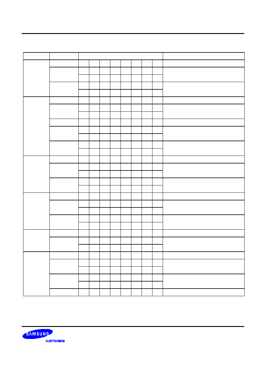
KS57C0502/C0504/P0504 MICROCONTROLLER
INSTRUCTION SET
519
Table 519. Arithmetic Instructions -- Binary Code Summary
Name
Operand
Binary Code
Operation Notation
ADC
A,@HL
0
0
1
1
1
1
1
0
C, A
A + (HL) + C
EA,RR
1
1
0
1
1
1
0
0
C, EA
EA + RR + C
1
0
1
0
1
r2
r1
0
RRb,EA
1
1
0
1
1
1
0
0
C, RRb
RRb + EA + C
1
0
1
0
0
r2
r1
0
ADS
A, #im
1
0
1
0
d3
d2
d1
d0
A
A + im; skip on carry
EA,#imm
1
1
0
0
1
0
0
1
EA
EA + imm; skip on carry
d7
d6
d5
d4
d3
d2
d1
d0
A,@HL
0
0
1
1
1
1
1
1
A
A + (HL); skip on carry
EA,RR
1
1
0
1
1
1
0
0
EA
EA + RR; skip on carry
1
0
0
1
1
r2
r1
0
RRb,EA
1
1
0
1
1
1
0
0
RRb
RRb + EA; skip on carry
1
0
0
1
0
r2
r1
0
SBC
A,@HL
0
0
1
1
1
1
0
0
C,A
A (HL) C
EA,RR
1
1
0
1
1
1
0
0
C, EA
EA RR C
1
1
0
0
1
r2
r1
0
RRb,EA
1
1
0
1
1
1
0
0
C,RRb
RRb EA C
1
1
0
0
0
r2
r1
0
SBS
A,@HL
0
0
1
1
1
1
0
1
A
A (HL); skip on borrow
EA,RR
1
1
0
1
1
1
0
0
EA
EA RR; skip on borrow
1
0
1
1
1
r2
r1
0
RRb,EA
1
1
0
1
1
1
0
0
RRb
RRb EA; skip on borrow
1
0
1
1
0
r2
r1
0
DECS
R
0
1
0
0
1
r2
r1
r0
R
R1; skip on borrow
RR
1
1
0
1
1
1
0
0
RR
RR1; skip on borrow
1
1
0
1
1
r2
r1
0
INCS
R
0
1
0
1
1
r2
r1
r0
R
R + 1; skip on carry
DA
1
1
0
0
1
0
1
0
DA
DA + 1; skip on carry
a7
a6
a5
a4
a3
a2
a1
a0
@HL
1
1
0
1
1
1
0
1
(HL)
(HL) + 1; skip on carry
0
1
1
0
0
0
1
0
RRb
1
0
0
0
0
r2
r1
0
RRb
RRb + 1; skip on carry
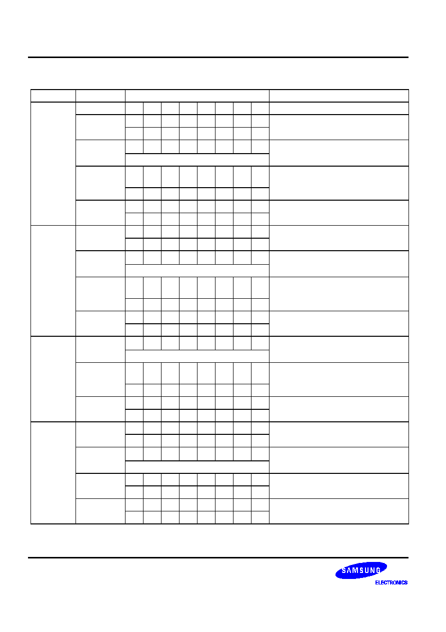
INSTRUCTION SET
KS57C0502/C0504/P0504 MICROCONTROLLER
520
Table 520. Bit Manipulation Instructions -- Binary Code Summary
Name
Operand
Binary Code
Operation Notation
BTST
C
1
1
0
1
0
1
1
1
Skip if C = 1
DA.b
1
1
b1
b0
0
0
1
1
Skip if DA.b = 1
a7
a6
a5
a4
a3
a2
a1
a0
mema.b
*
1
1
1
1
1
0
0
1
Skip if mema.b = 1
memb.@L
1
1
1
1
1
0
0
1
Skip if [memb.72 + L.32].
[L.10] = 1
0
1
0
0
a5
a4
a3
a2
@H+DA.b
1
1
1
1
1
0
0
1
Skip if [H + DA.30].b = 1
0
0
b1
b0
a3
a2
a1
a0
BTSF
DA.b
1
1
b1
b0
0
0
1
0
Skip if DA.b = 0
a7
a6
a5
a4
a3
a2
a1
a0
mema.b
*
1
1
1
1
1
0
0
0
Skip if mema.b = 0
memb.@L
1
1
1
1
1
0
0
0
Skip if [memb.72 + L.32].
[L.10] = 0
0
1
0
0
a5
a4
a3
a2
@H+DA.b
1
1
1
1
1
0
0
0
Skip if [H + DA.30].b = 0
0
0
b1
b0
a3
a2
a1
a0
BTSTZ
mema.b
*
1
1
1
1
1
1
0
1
Skip if mema.b = 1 and clear
memb.@L
1
1
1
1
1
1
0
1
Skip if [memb.72 + L.32].
[L.10] = 1 and clear
0
1
0
0
a5
a4
a3
a2
@H+DA.b
1
1
1
1
1
1
0
1
Skip if [H + DA.30].b =1 and clear
0
0
b1
b0
a3
a2
a1
a0
BITS
DA.b
1
1
b1
b0
0
0
0
1
DA.b
1
a7
a6
a5
a4
a3
a2
a1
a0
mema.b
*
1
1
1
1
1
1
1
1
mema.b
1
memb.@L
1
1
1
1
1
1
1
1
[memb.72 + L.32].b [L.10]
1
0
1
0
0
a5
a4
a3
a2
@H+DA.b
1
1
1
1
1
1
1
1
[H + DA.30].b
1
0
0
b1
b0
a3
a2
a1
a0
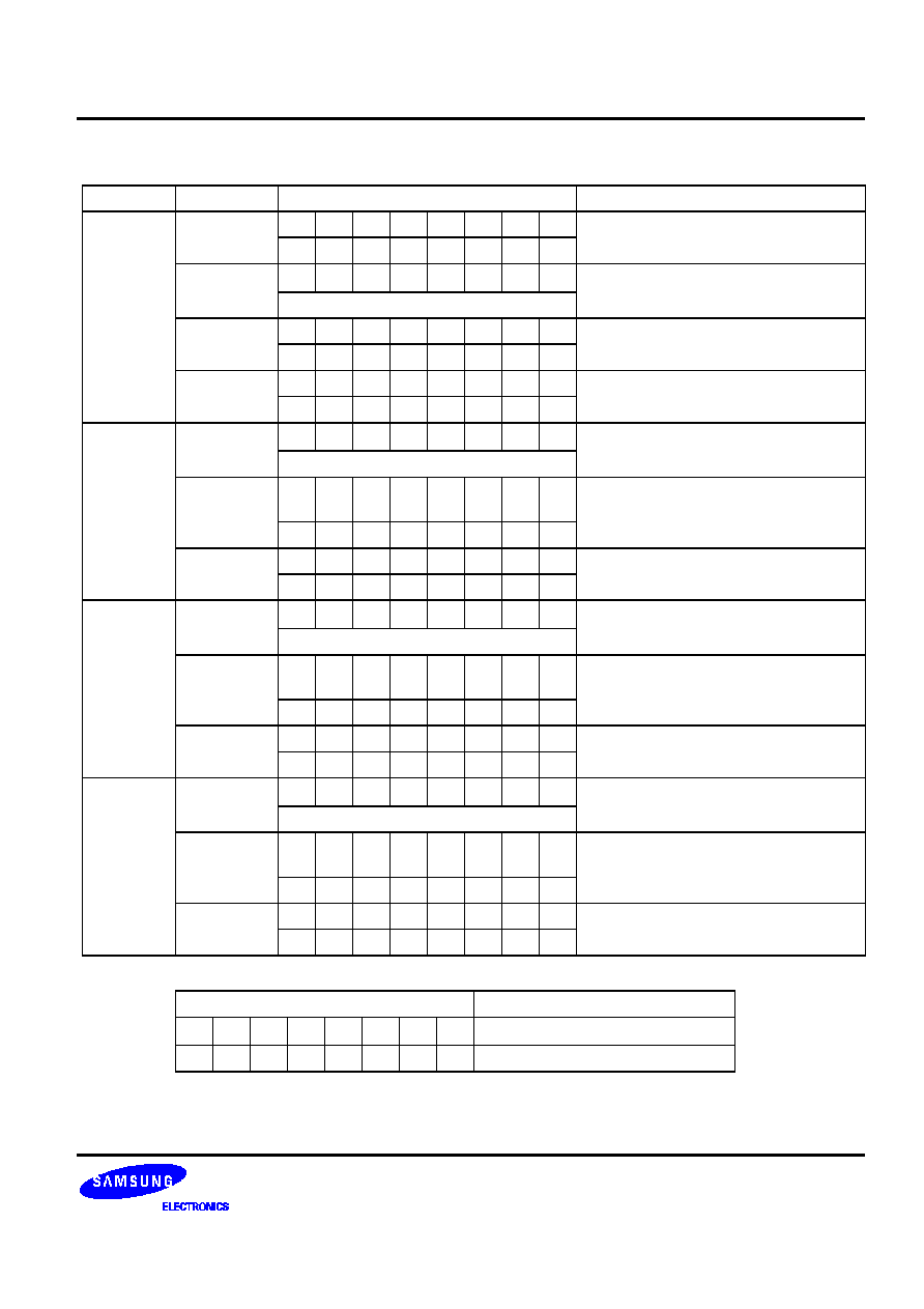
KS57C0502/C0504/P0504 MICROCONTROLLER
INSTRUCTION SET
521
Table 520. Bit Manipulation Instructions -- Binary Code Summary (Continued)
Name
Operand
Binary Code
Operation Notation
BITR
DA.b
1
1
b1
b0
0
0
0
0
DA.b
0
a7
a6
a5
a4
a3
a2
a1
a0
mema.b
*
1
1
1
1
1
1
1
0
mema.b
0
memb.@L
1
1
1
1
1
1
1
0
[memb.72 + L32].[L.10]
0
0
1
0
0
a5
a4
a3
a2
@H+DA.b
1
1
1
1
1
1
1
0
[H + DA.30].b
0
0
0
b1
b0
a3
a2
a1
a0
BAND
C,mema.b
*
1
1
1
1
0
1
0
1
C
C AND mema.b
C,memb.@L
1
1
1
1
0
1
0
1
C
C AND [memb.72 + L.32].
[L.10]
0
1
0
0
a5
a4
a3
a2
C,@H+DA.b
1
1
1
1
0
1
0
1
C
C AND [H + DA.30].b
0
0
b1
b0
a3
a2
a1
a0
BOR
C,mema.b
*
1
1
1
1
0
1
1
0
C
C OR mema.b
C,memb.@L
1
1
1
1
0
1
1
0
C
C OR [memb.72 + L.32].
[L.10]
0
1
0
0
a5
a4
a3
a2
C,@H+DA.b
1
1
1
1
0
1
1
0
C
C OR [H + DA.30].b
0
0
b1
b0
a3
a2
a1
a0
BXOR
C,mema.b
*
1
1
1
1
0
1
1
1
C
C XOR mema.b
C,memb.@L
1
1
1
1
0
1
1
1
C
C XOR [memb.72 + L.32].
[L.10]
0
1
0
0
a5
a4
a3
a2
C,@H+DA.b
1
1
1
1
0
1
1
1
C
C XOR [H + DA.30].b
0
0
b1
b0
a3
a2
a1
a0
Second Byte
Bit Addresses
*
mema.b
1
0
b1
b0
a3
a2
a1
a0
FB0HFBFH
1
1
b1
b0
a3
a2
a1
a0
FF0HFFFH
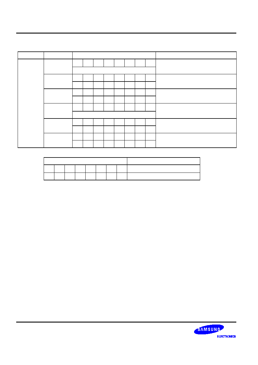
INSTRUCTION SET
KS57C0502/C0504/P0504 MICROCONTROLLER
522
Table 520. Bit Manipulation Instructions -- Binary Code Summary (Concluded)
Name
Operand
Binary Code
Operation Notation
LDB
mema.b,C
*
1
1
1
1
1
1
0
0
mema.b
C
memb.@L,C
1
1
1
1
1
1
0
0
memb.72 + [L.32]. [L.10]
C
0
1
0
0
a5
a4
a3
a2
@H+DA.b,C
1
1
1
1
1
1
0
0
H + [DA.30].b
(C)
0
b2
b1
b0
a3
a2
a1
a0
C,mema.b
*
1
1
1
1
0
1
0
0
C
mema.b
C,memb.@L
1
1
1
1
0
1
0
0
C
memb.72 + [L.32] . [L.10]
0
1
0
0
a5
a4
a3
a2
C,@H+DA.b
1
1
1
1
0
1
0
0
C
[H + DA.30].b
0
b2
b1
b0
a3
a2
a1
a0
Second Byte
Bit Addresses
*
mema.b
1
0
b1
b0
a3
a2
a1
a0
FB0HFBFH
1
1
b1
b0
a3
a2
a1
a0
FF0HFFFH

KS57C0502/C0504/P0504 MICROCONTROLLER
INSTRUCTION SET
523
INSTRUCTION DESCRIPTIONS
The following section contains detailed information and programming examples for each instruction of the
SAM47 instruction set. Information is arranged in a consistent format to improve readability and for use as a
quick-reference resource for application programmers.
If you are reading this user's manual for the first time, please just scan this very detailed information in order to
acquaint yourself with the basic features of the instruction set. The information elements of the instruction
description format are as follows:
--
Instruction name (mnemonic)
--
Full instruction name
--
Source/destination format of the instruction operand
--
Operation overview (from the "High-Level Summary" table)
--
Textual description of the instruction's effect
--
Binary code overview (from the "Binary Code Summary" table)
--
Programming example(s) to show how the instruction is used
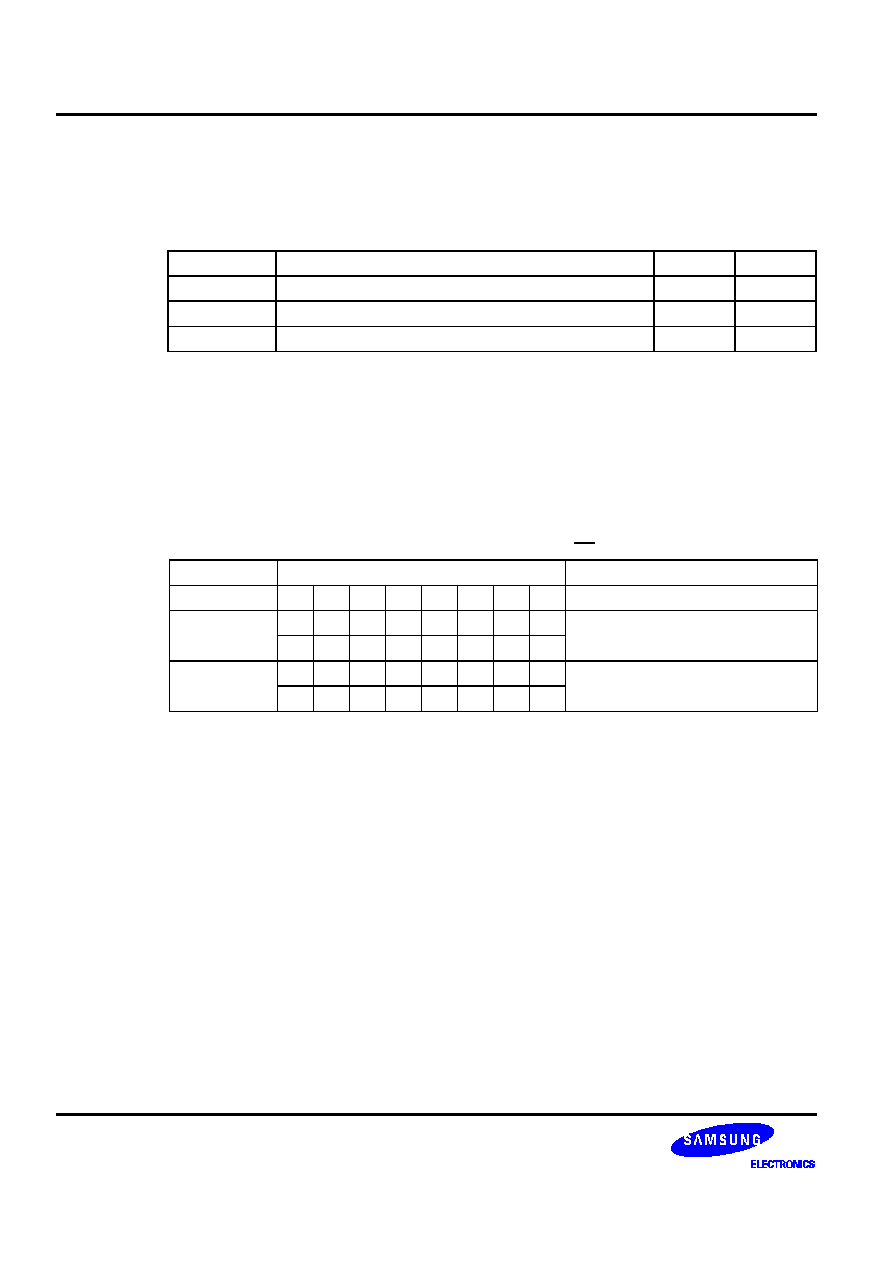
INSTRUCTION SET
KS57C0502/C0504/P0504 MICROCONTROLLER
524
ADC
Add with Carry
ADC
dst,src
Operation:
Operand
Operation Summary
Bytes
Cycles
A,@HL
Add indirect data memory to A with carry
1
1
EA,RR
Add register pair (RR) to EA with carry
2
2
RRb,EA
Add EA to register pair (RRb) with carry
2
2
Description:
The source operand, along with the setting of the carry flag, is added to the destination operand
and the sum is stored in the destination. The contents of the source are unaffected. If there is an
overflow from the most significant bit of the result, the carry flag is set; otherwise, the carry flag
is cleared.
If 'ADC A,@HL' is followed by an 'ADS A,#im' instruction in a program, ADC skips the ADS
instruction if an overflow occurs. If there is no overflow, the ADS instruction is executed
normally. (This condition is valid only for 'ADC A,@HL' instructions. If an overflow occurs
following an 'ADS A,#im' instruction, the next instruction will not be skipped.)
Operand
Binary Code
Operation Notation
A,@HL
0
0
1
1
1
1
1
0
C, A
A + (HL) + C
EA,RR
1
1
0
1
1
1
0
0
C, EA
EA + RR + C
1
0
1
0
1
r2
r1
0
RRb,EA
1
1
0
1
1
1
0
0
C, RRb
RRb + EA + C
1
0
1
0
0
r2
r1
0
Examples:
1.
The extended accumulator contains the value 0C3H, register pair HL the value 0AAH, and
the carry flag is set to "1":
SCF
; C
"1"
ADC
EA,HL
; EA
0C3H + 0AAH + 1H = 6EH, C
"1"
JPS
XXX
; Jump to XXX; no skip after ADC
2.
If the extended accumulator contains the value 0C3H, register pair HL the value 0AAH, and
the carry flag is cleared to "0":
RCF
; C
"0"
ADC
EA,HL
; EA
0C3H + 0AAH + 0H = 6EH, C
"1"
JPS
XXX
; Jump to XXX; no skip after ADC

KS57C0502/C0504/P0504 MICROCONTROLLER
INSTRUCTION SET
525
ADC
Add with Carry
ADC
(Continued)
Examples:
3.
If ADC A,@HL is followed by an ADS A,#im, the ADC skips on carry to the instruction
immediately after the ADS. An ADS instruction immediately after the ADC does not skip
even
if an overflow occurs. This function is useful for decimal adjustment operations.
a.
8 + 9 decimal addition (the contents of the address specified by the HL register is 9H):
RCF
; C
"0"
LD
A,#8H
; A
8H
ADS
A,#6H
; A
8H + 6H = 0EH
ADC
A,@HL
; A
7H, C
"1"
ADS
A,#0AH
; Skip this instruction because C = "1" after ADC result
JPS
XXX
b.
3 + 4 decimal addition (the contents of the address specified by the HL register is 4H):
RCF
; C
"0"
LD
A,#3H
; A
3H
ADS
A,#6H
; A
3H + 6H = 9H
ADC
A,@HL
; A
9H + 4H + C(0) = 0DH
ADS
A,#0AH
; No skip. A
0DH + 0AH = 7H
; (The skip function for 'ADS A,#im' is inhibited after an
; 'ADC A,@HL' instruction even if an overflow occurs.)
JPS
XXX
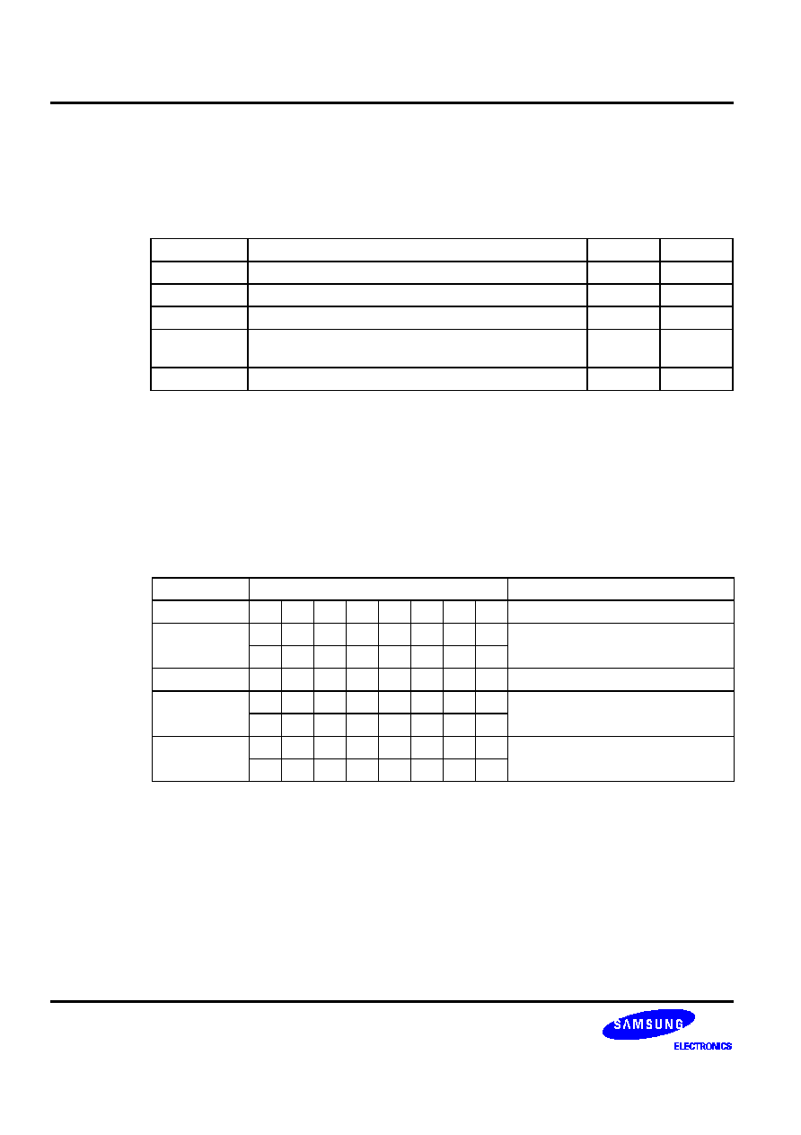
INSTRUCTION SET
KS57C0502/C0504/P0504 MICROCONTROLLER
526
ADS
Add and Skip on Overflow
ADS
dst,src
Operation:
Operand
Operation Summary
Bytes
Cycles
A, #im
Add 4-bit immediate data to A and skip on overflow
1
1 + S
EA,#imm
Add 8-bit immediate data to EA and skip on overflow
2
2 + S
A,@HL
Add indirect data memory to A and skip on overflow
1
1 + S
EA,RR
Add register pair (RR) contents to EA and skip on
overflow
2
2 + S
RRb,EA
Add EA to register pair (RRb) and skip on overflow
2
2 + S
Description:
The source operand is added to the destination operand and the sum is stored in the destination.
The contents of the source are unaffected. If there is an overflow from the most significant bit of
the result, the skip signal is generated and a skip is executed, but the carry flag value is
unaffected.
If 'ADS A,#im' follows an 'ADC A,@HL' instruction in a program, ADC skips the ADS instruction
if an overflow occurs. If there is no overflow, the ADS instruction is executed normally. This skip
condition is valid only for 'ADC A,@HL' instructions, however. If an overflow occurs following an
ADS instruction, the next instruction is not skipped.
Operand
Binary Code
Operation Notation
A, #im
1
0
1
0
d3
d2
d1
d0
A
A + im; skip on overflow
EA,#imm
1
1
0
0
1
0
0
1
EA
EA + imm; skip on overflow
d7
d6
d5
d4
d3
d2
d1
d0
A,@HL
0
0
1
1
1
1
1
1
A
A + (HL); skip on overflow
EA,RR
1
1
0
1
1
1
0
0
EA
EA + RR; skip on overflow
1
0
0
1
1
r2
r1
0
RRb,EA
1
1
0
1
1
1
0
0
RRb
RRb + EA; skip on overflow
1
0
0
1
0
r2
r1
0
Examples:
1.
The extended accumulator contains the value 0C3H, register pair HL the value 0AAH, and
the carry flag = "0":
ADS
EA,HL
; EA
0C3H + 0AAH = 6DH, C
"0"
; ADS skips on overflow, but carry flag value is not affected.
JPS
XXX
; This instruction is skipped because ADS overflowed.
JPS
YYY
; Jump to YYY.

KS57C0502/C0504/P0504 MICROCONTROLLER
INSTRUCTION SET
527
ADS
Add and Skip on Overflow
ADS
(Continued)
Examples:
2.
If the extended accumulator contains the value 0C3H, register pair HL the value 12H, and
the carry flag = "0":
ADS
EA,HL
; EA
0C3H + 12H = 0D5H, C
"0"
JPS
XXX
; Jump to XXX; no skip after ADS.
3.
If 'ADC A,@HL' is followed by an 'ADS A,#im', the ADC skips on overflow to the instruction
immediately after the ADS. An 'ADS A,#im' instruction immediately after the 'ADC A,@HL'
does not skip even if overflow occurs. This function is useful for decimal adjustment
operations.
a.
8 + 9 decimal addition (the contents of the address specified by the HL register is 9H):
RCF
; C
"0"
LD
A,#8H
; A
8H
ADS
A,#6H
; A
8H + 6H = 0EH
ADC
A,@HL
; A
7H, C
"1"
ADS
A,#0AH
; Skip this instruction because C = "1" after ADC result.
JPS
XXX
b.
3 + 4 decimal addition (the contents of the address specified by the HL register is 4H):
RCF
; C
"0"
LD
A,#3H
; A
3H
ADS
A,#6H
; A
3H + 6H = 9H
ADC
A,@HL
; A
9H + 4H + C(0) = 0DH
ADS
A,#0AH
; No skip. A
0DH + 0AH = 7H
; (The skip function for 'ADS A,#im' is inhibited after an
; 'ADC A,@HL' instruction even if an overflow occurs.)
JPS
XXX
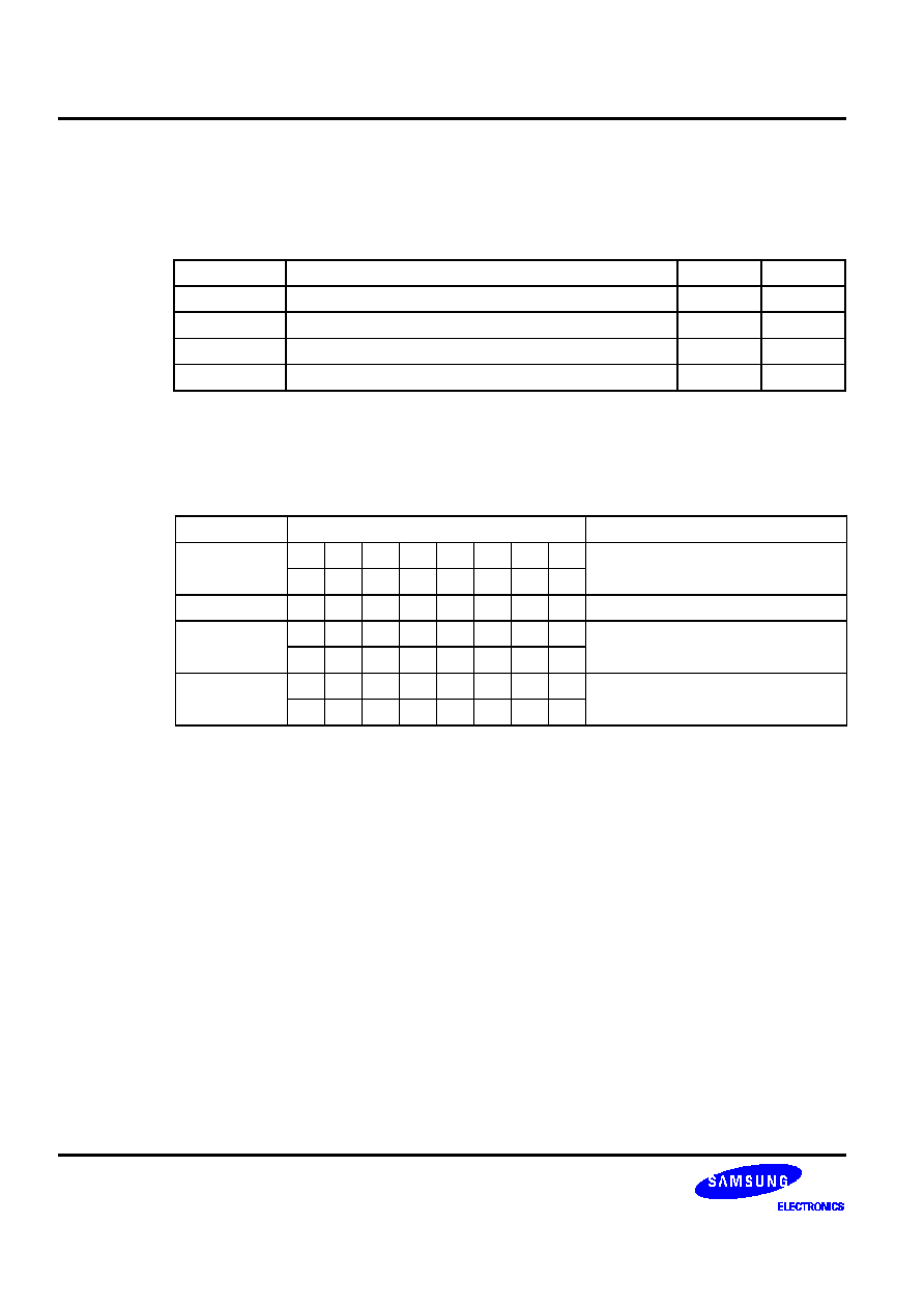
INSTRUCTION SET
KS57C0502/C0504/P0504 MICROCONTROLLER
528
AND
Logical AND
AND
dst,src
Operation:
Operand
Operation Summary
Bytes
Cycles
A,#im
Logical-AND A immediate data to A
2
2
A,@HL
Logical-AND A indirect data memory to A
1
1
EA,RR
Logical-AND register pair (RR) to EA
2
2
RRb,EA
Logical-AND EA to register pair (RRb)
2
2
Description:
The source operand is logically ANDed with the destination operand. The result is stored in the
destination. The logical AND operation results in a "1" bit being stored whenever the
corresponding bits in the two operands are both "1"; otherwise a "0" bit is stored. The contents of
the source are unaffected.
Operand
Binary Code
Operation Notation
A,#im
1
1
0
1
1
1
0
1
A
A AND im
0
0
0
1
d3
d2
d1
d0
A,@HL
0
0
1
1
1
0
0
1
A
A AND (HL)
EA,RR
1
1
0
1
1
1
0
0
EA
EA AND RR
0
0
0
1
1
r2
r1
0
RRb,EA
1
1
0
1
1
1
0
0
RRb
RRb AND EA
0
0
0
1
0
r2
r1
0
Example:
If the extended accumulator contains the value 0C3H (11000011B) and register pair HL the
value 55H (01010101B), the instruction
AND
EA,HL
leaves the value 41H (01000001B) in the extended accumulator EA .
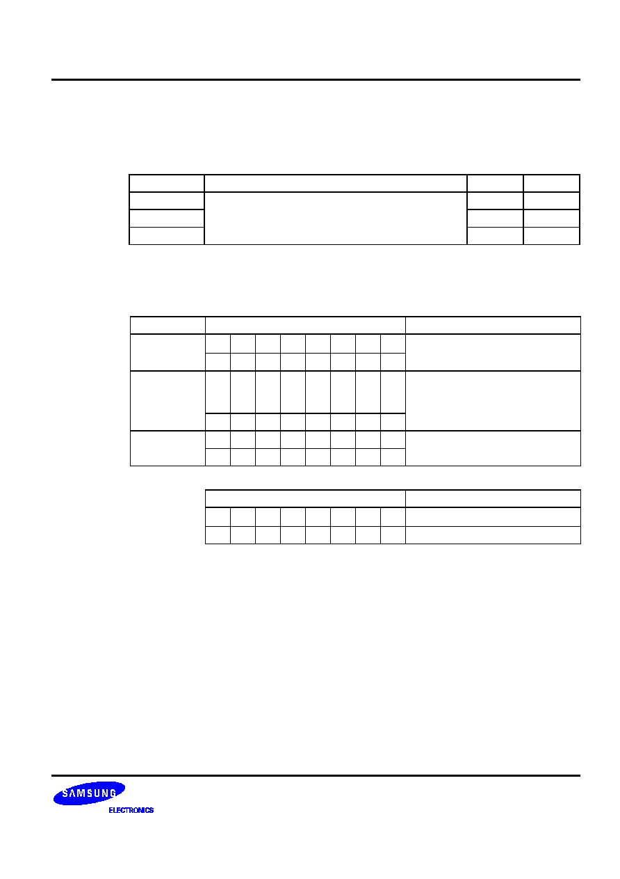
KS57C0502/C0504/P0504 MICROCONTROLLER
INSTRUCTION SET
529
BAND
Bit Logical AND
BAND
C,src.b
Operation:
Operand
Operation Summary
Bytes
Cycles
C,mema.b
Logical-AND carry flag with memory bit
2
2
C,memb.@L
2
2
C,@H+DA.b
2
2
Description:
The specified bit of the source is logically ANDed with the carry flag bit value. If the Boolean
value of the source bit is a logic zero, the carry flag is cleared to "0"; otherwise, the current carry
flag setting is left unaltered. The bit value of the source operand is not affected.
Operand
Binary Code
Operation Notation
C,mema.b
*
1
1
1
1
0
1
0
1
C
C AND mema.b
C,memb.@L
1
1
1
1
0
1
0
1
C
C AND [memb.72 + L.3
2].
[L.10]
0
1
0
0
a5
a4
a3
a2
C,@H+DA.b
1
1
1
1
0
1
0
1
C
C AND [H + DA.30].b
0
0
b1
b0
a3
a2
a1
a0
Second Byte
Bit Addresses
*
mema.b
1
0
b1
b0
a3
a2
a1
a0
FB0HFBFH
1
1
b1
b0
a3
a2
a1
a0
FF0HFFFH
Examples:
1.
The following instructions set the carry flag if P1.0 (port 1.0) is equal to "1" (and assuming
the carry flag is already set to "1"):
SMB
15
; C
"1"
BAND
C,P1.0
; If P1.0 = "1", C
"1"
; If P1.0 = "0", C
"0"

INSTRUCTION SET
KS57C0502/C0504/P0504 MICROCONTROLLER
530
BAND
Bit Logical AND
BAND
(Continued)
Examples:
2.
Assume the P1 address is FF1H and the value for register L is 9H (1001B). The address
(memb.72) is 111100B; (L.32) is 10B. The resulting address is 11110010B or FF2H,
specifying P2. The bit value for the BAND instruction, (L.10) is 01B which specifies bit 1.
Therefore, P1.@L = P2.1:
LD
L,#9H
BAND
C,P1.@L
; P1.@L is specified as P2.1
; C AND P2.1
3.
Register H contains the value 2H and FLAG = 20H.3. The address of H is 0010B and
FLAG(30) is 0000B. The resulting address is 00100000B or 20H. The bit value for the
BAND instruction is 3. Therefore, @H+FLAG = 20H.3:
FLAG
EQU
20H.3
LD
H,#2H
BAND
C,@H+FLAG
; C AND FLAG (20H.3)
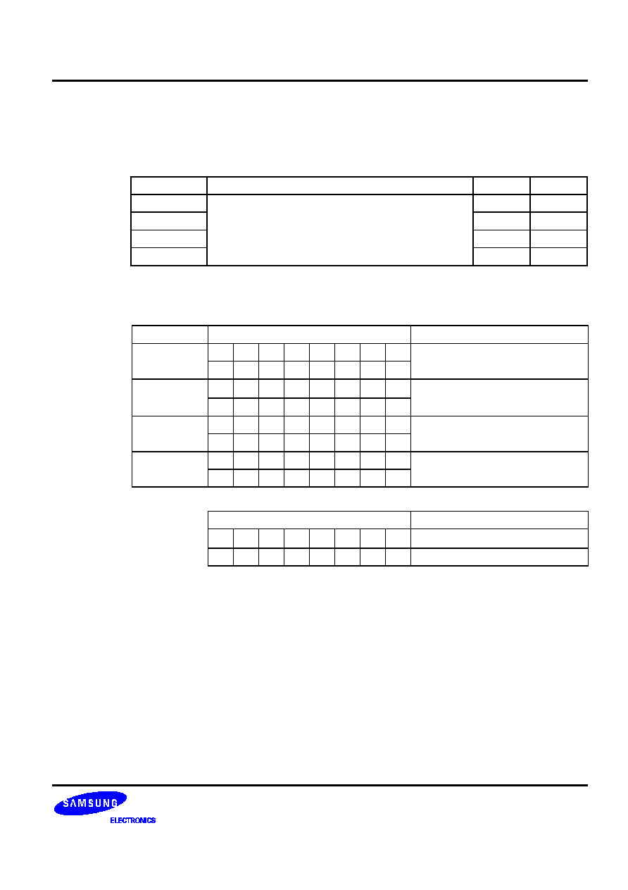
KS57C0502/C0504/P0504 MICROCONTROLLER
INSTRUCTION SET
531
BITR
Bit Reset
BITR
dst.b
Operation:
Operand
Operation Summary
Bytes
Cycles
DA.b
Clear specified memory bit to logic zero
2
2
mema.b
2
2
memb.@L
2
2
@H+DA.b
2
2
Description:
A BITR instruction clears to logic zero (resets) the specified bit within the destination operand.
No other bits in the destination are affected.
Operand
Binary Code
Operation Notation
DA.b
1
1
b1
b0
0
0
0
0
DA.b
0
a7
a6
a5
a4
a3
a2
a1
a0
mema.b
*
1
1
1
1
1
1
1
0
mema.b
0
memb.@L
1
1
1
1
1
1
1
0
[memb.72 + L32].[L.10]
0
0
1
0
0
a5
a4
a3
a2
@H+DA.b
1
1
1
1
1
1
1
0
[H + DA.30].b
0
0
0
b1
b0
a3
a2
a1
a0
Second Byte
Bit Addresses
*
mema.b
1
0
b1
b0
a3
a2
a1
a0
FB0HFBFH
1
1
b1
b0
a3
a2
a1
a0
FF0HFFFH
Examples:
1.
Bit location 30H.2 in the RAM has a current value of logic one. The following instruction
clears the third bit in RAM location 30H (bit 2) to logic zero:
BITR
30H.2
; 30H.2
"0"
2.
You can use BITR in the same way to manipulate a port address bit:
BITR
P2.0
; P2.0
"0"

INSTRUCTION SET
KS57C0502/C0504/P0504 MICROCONTROLLER
532
BITR
Bit Reset
BITR
(Continued)
Examples:
3.
Assuming that P2.2, P2.3, and P3.0P3.3 are cleared to "0":
LD
L,#0AH
BP2
BITR
P0.@L
; First, P0.@0AH = P2.2
; (111100B) + 10B.10B = 0F2H.2
INCS
L
JR
BP2
4.
If bank 0, location 0A0H.0 is cleared (and regardless of whether the EMB value is logic
zero), BITR has the following effect:
FLAG
EQU
0A0H.0
·
·
·
BITR
EMB
·
·
·
LD
H,#0AH
BITR
@H+FLAG
; Bank 0 (AH + 0H).0 = 0A0H.0
"0"
NOTE
Because the BITR instruction is used for output functions, the pin names used in the examples
above may vary for different devices in the SAM47 product family.
KS57C0502/C0504/P0504 MICROCONTROLLER
INSTRUCTION SET
533
BITS
Bit Set
BITS
dst.b
Operation:
Operand
Operation Summary
Bytes
Cycles
DA.b
Set specified memory bit
2
2
mema.b
2
2
memb.@L
2
2
@H+DA.b
2
2
Description:
This instruction sets the specified bit within the destination without affecting any other bits in the
destination. BITS can manipulate any bit that is addressable using direct or indirect addressing
modes.
Operand
Binary Code
Operation Notation
DA.b
1
1
b1
b0
0
0
0
1
DA.b
1
a7
a6
a5
a4
a3
a2
a1
a0
mema.b
*
1
1
1
1
1
1
1
1
mema.b
1
memb.@L
1
1
1
1
1
1
1
1
[memb.72 + L.32].b [L.10]
1
0
1
0
0
a5
a4
a3
a2
@H+DA.b
1
1
1
1
1
1
1
1
[H + DA.30].b
1
0
0
b1
b0
a3
a2
a1
a0
Second Byte
Bit Addresses
*
mema.b
1
0
b1
b0
a3
a2
a1
a0
FB0HFBFH
1
1
b1
b0
a3
a2
a1
a0
FF0HFFFH
Examples:
1.
Assuming that bit location 30H.2 in the RAM has a current value of "0", the following
instruction sets the second bit of location 30H to "1".
BITS
30H.2
; 30H.2
"1"
2.
You can use BITS in the same way to manipulate a port address bit:
BITS
P2.0
; P2.0
"1"

INSTRUCTION SET
KS57C0502/C0504/P0504 MICROCONTROLLER
534
BITS
Bit Set
BITS
(Continued)
Examples:
3.
Given that P2.2, P2.3, and P3.0P3.3 are set to "1":
LD
L,#0AH
BP2
BITS
P0.@L
; First, P0.@0AH = P2.2
; (111100B) + 10B.10B = 0F2H.2
INCS
L
JR
BP2
4.
If bank 0, location 0A0H.0, is set to "1" and the EMB = "0", BITS has the following effect:
FLAG
EQU
0A0H.0
·
·
·
BITR
EMB
·
·
·
LD
H,#0AH
BITS
@H+FLAG
; Bank 0 (AH + 0H).0 = 0A0H.0
"1"
NOTE
Because the BITS instruction is used for output functions, pin names used in the examples
above may vary for different devices in the SAM47 product family.
KS57C0502/C0504/P0504 MICROCONTROLLER
INSTRUCTION SET
535
BOR
Bit Logical OR
BOR
C,src.b
Operation:
Operand
Operation Summary
Bytes
Cycles
C,mema.b
Logical-OR carry with specified memory bit
2
2
C,memb.@L
2
2
C,@H+DA.b
2
2
Description:
The specified bit of the source is logically ORed with the carry flag bit value. The value of the
source is unaffected.
Operand
Binary Code
Operation Notation
C,mema.b
*
1
1
1
1
0
1
1
0
C
C OR mema.b
C,memb.@L
1
1
1
1
0
1
1
0
C
C OR [memb.72 + L.32].
[L.10]
0
1
0
0
a5
a4
a3
a2
C,@H+DA.b
1
1
1
1
0
1
1
0
C
C OR [H + DA.30].b
0
0
b1
b0
a3
a2
a1
a0
Second Byte
Bit Addresses
*
mema.b
1
0
b1
b0
a3
a2
a1
a0
FB0HFBFH
1
1
b1
b0
a3
a2
a1
a0
FF0HFFFH
Examples:
1.
The carry flag is logically ORed with the P1.0 value:
RCF
; C
"0"
BOR
C,P1.0
; If P1.0 = "1", then C
"1"; if P1.0 = "0", then C
"0"
2.
The P1 address is FF1H and register L contains the value 9H (1001B). The address
(memb.72) is 111100B and (L.32) = 10B. The resulting address is 11110010B or FF2H,
specifying P2. The bit value for the BOR instruction, (L.10) is 01B which specifies bit 1.
Therefore, P1.@L = P2.1:
LD
L,#9H
BOR
C,P1.@L
; P1.@L is specified as P2.1; C OR P2.1

INSTRUCTION SET
KS57C0502/C0504/P0504 MICROCONTROLLER
536
BOR
Bit Logical OR
BOR
(Continued)
Examples:
3.
Register H contains the value 2H and FLAG = 20H.3. The address of H is 0010B and
FLAG(30) is 0000B. The resulting address is 00100000B or 20H. The bit value for the BOR
instruction is 3. Therefore, @H+FLAG = 20H.3:
FLAG
EQU
20H.3
LD
H,#2H
BOR
C,@H+FLAG
;
C OR FLAG (20H.3)

KS57C0502/C0504/P0504 MICROCONTROLLER
INSTRUCTION SET
537
BTSF
Bit Test Skip on False
BTSF
dst.b
Operation:
Operand
Operation Summary
Bytes
Cycles
DA.b
Test specified memory bit and skip if bit equals "0"
2
2 + S
mema.b
2
2 + S
memb.@L
2
2 + S
@H+DA.b
2
2 + S
Description:
The specified bit within the destination operand is tested. If it is a "0", the BTSF instruction skips
the instruction which immediately follows it; otherwise the instruction following the BTSF is
executed. The destination bit value is not affected.
Operand
Binary Code
Operation Notation
DA.b
1
1
b1
b0
0
0
1
0
Skip if DA.b = 0
a7
a6
a5
a4
a3
a2
a1
a0
mema.b
*
1
1
1
1
1
0
0
0
Skip if mema.b = 0
memb.@L
1
1
1
1
1
0
0
0
Skip if [memb.72 + L.3-2].
[L.10] = 0
0
1
0
0
a5
a4
a3
a2
@H + DA.b
1
1
1
1
1
0
0
0
Skip if [H + DA.30].b = 0
0
0
b1
b0
a3
a2
a1
a0
Second Byte
Bit Addresses
*
mema.b
1
0
b1
b0
a3
a2
a1
a0
FB0HFBFH
1
1
b1
b0
a3
a2
a1
a0
FF0HFFFH
Examples:
1.
If RAM bit location 30H.2 is set to logic zero, the following instruction sequence will cause
the program to continue execution from the instruction identifed as LABEL2:
BTSF
30H.2
; If 30H.2 = "0", then skip
RET
; If 30H.2 = "1", return
JP
LABEL2
2.
You can use BTSF in the same way to manipulate a port pin address bit:
BTSF
P2.0
; If P2.0 = "0", then skip
RET
; If P2.0 = "1", then return
JP
LABEL3

INSTRUCTION SET
KS57C0502/C0504/P0504 MICROCONTROLLER
538
BTSF
Bit Test and Skip on False
BTSF
(Continued)
Examples:
3.
P2.2, P2.3 and P3.0P3.3 are tested:
LD
L,#0AH
BP2
BTSF
P0.@L
; First, P0.@0AH = P2.2
; (111100B) + 10B.10B = 0F2H.2
RET
INCS
L
JR
BP2
4.
Bank 0, location 0A0H.0, is tested and (regardless of the current EMB value) BTSF has the
following effect:
FLAG
EQU
0A0H.0
·
·
·
BITR
EMB
·
·
·
LD
H,#0AH
BTSF
@H+FLAG
; If bank 0 (AH + 0H).0 = 0A0H.0 =
"0", then skip
RET
·
·
·
KS57C0502/C0504/P0504 MICROCONTROLLER
INSTRUCTION SET
539
BTST
Bit Test and Skip on True
BTST
dst.b
Operation:
Operand
Operation Summary
Bytes
Cycles
C
Test carry bit and skip if set (= "1")
1
1 + S
DA.b
Test specified bit and skip if memory bit is set
2
2 + S
mema.b
2
2 + S
memb.@L
2
2 + S
@H+DA.b
2
2 + S
Description:
The specified bit within the destination operand is tested. If it is "1", the instruction that
immediately follows the BTST instruction is skipped; otherwise the instruction following the BTST
instruction is executed. The destination bit value is not affected.
Operand
Binary Code
Operation Notation
C
1
1
0
1
0
1
1
1
Skip if C = 1
DA.b
1
1
b1
b0
0
0
1
1
Skip if DA.b = 1
a7
a6
a5
a4
a3
a2
a1
a0
mema.b
*
1
1
1
1
1
0
0
1
Skip if mema.b = 1
memb.@L
1
1
1
1
1
0
0
1
Skip if [memb.72 + L.32].
[L.10] = 1
0
1
0
0
a5
a4
a3
a2
@H+DA.b
1
1
1
1
1
0
0
1
Skip if [H + DA.30].b = 1
0
0
b1
b0
a3
a2
a1
a0
Second Byte
Bit Addresses
*
mema.b
1
0
b1
b0
a3
a2
a1
a0
FB0HFBFH
1
1
b1
b0
a3
a2
a1
a0
FF0HFFFH
Examples:
1.
If RAM bit location 30H.2 is set to logic zero, the following instruction sequence will execute
the RET instruction:
BTST
30H.2
; If 30H.2 = "1", then skip
RET
; If 30H.2 = "0", return
JP
LABEL2

INSTRUCTION SET
KS57C0502/C0504/P0504 MICROCONTROLLER
540
BTST
Bit Test and Skip on True
BTST
(Continued)
Examples:
2.
You can use BTST in the same way to manipulate a port pin address bit:
BTST
P2.0
; If P2.0 = "1", then skip
RET
; If P2.0 = "0", then return
JP
LABEL3
3.
Assume that P2.2, P2.3 and P3.0P3.3 are cleared to "0":
LD
L,#0AH
BP2
BTST
P0.@L
; First, P0.@0AH = P2.2
; (111100B) + 10B.10B = 0F2H.2
RET
INCS
L
JR
BP2
4.
Bank 0, location 0A0H.0, is tested and (regardless of the current EMB value) BTST has the
following effect:
FLAG
EQU
0A0H.0
·
·
·
BITR
EMB
·
·
·
LD
H,#0AH
BTST
@H+FLAG
; If bank 0 (AH + 0H).0 = 0A0H.0 =
"1", then skip
RET
·
·
·
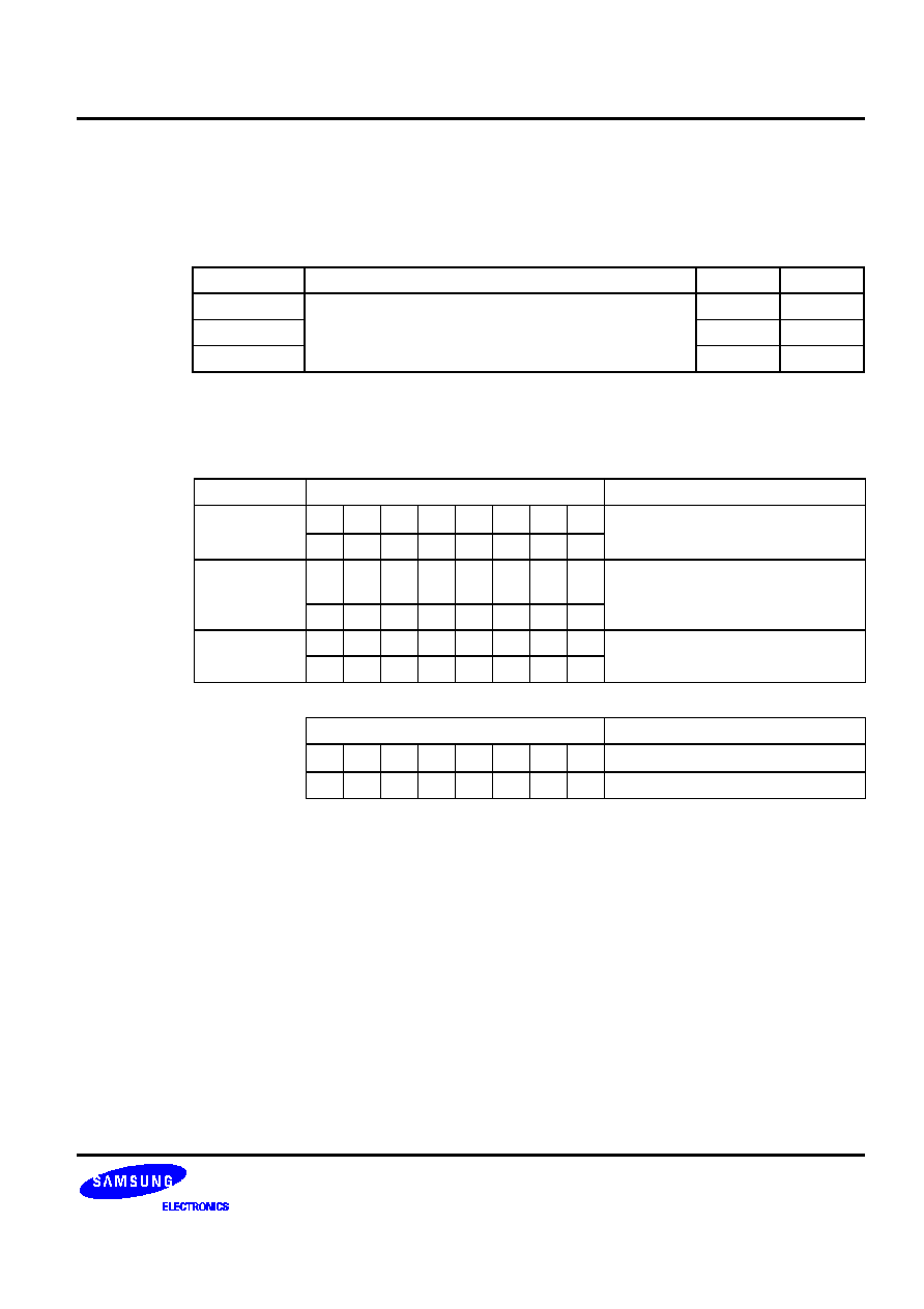
KS57C0502/C0504/P0504 MICROCONTROLLER
INSTRUCTION SET
541
BTSTZ
Bit Test and Skip on True; Clear Bit
BTSTZ
dst.b
Operation:
Operand
Operation Summary
Bytes
Cycles
mema.b
Test specified bit; skip and clear if memory bit is set
2
2 + S
memb.@L
2
2 + S
@H+DA.b
2
2 + S
Description:
The specified bit within the destination operand is tested. If it is a "1", the instruction immediately
following the BTSTZ instruction is skipped; otherwise the instruction following the BTSTZ is
executed. The destination bit value is cleared.
Operand
Binary Code
Operation Notation
mema.b
*
1
1
1
1
1
1
0
1
Skip if mema.b = 1 and clear
memb.@L
1
1
1
1
1
1
0
1
Skip if [memb.72 + L.32].
[L.10] = 1 and clear
0
1
0
0
a5
a4
a3
a2
@H+DA.b
1
1
1
1
1
1
0
1
Skip if [H + DA.30].b =1 and clear
0
0
b1
b0
a3
a2
a1
a0
Second Byte
Bit Addresses
*
mema.b
1
0
b1
b0
a3
a2
a1
a0
FB0HFBFH
1
1
b1
b0
a3
a2
a1
a0
FF0HFFFH
Examples:
1.
Port pin P2.0 is toggled by checking the P2.0 value (level):
BTSTZ
P2.0
; If P2.0 = "1", then P2.0
"0" and skip
BITS
P2.0
; If P2.0 = "0", then P2.0
"1"
JP
LABEL3
2.
Assume that port pins P2.2, P2.3 and P3.0P3.3 are toggled:
LD
L,#0AH
BP2
BTSTZ
P0.@L
; First, P0.@0AH = P2.2
; (111100B) + 10B.10B = 0F2H.2
RET
INCS
L
JR
BP2

INSTRUCTION SET
KS57C0502/C0504/P0504 MICROCONTROLLER
542
BTSTZ
Bit Test and Skip on True; Clear Bit
BTSTZ
(Continued)
Examples:
3.
Bank 0, location 0A0H.0, is tested and EMB = "0":
FLAG
EQU
0A0H.0
·
·
·
BITR
EMB
·
·
·
LD
H,#0AH
BTSTZ
@H+FLAG
;
If bank 0 (AH + 0H).0 = 0A0H.0 =
"1", clear and skip
BITS
@H+FLAG
;
If 0A0H.0 =
"0", then 0A0H.0
"1"

KS57C0502/C0504/P0504 MICROCONTROLLER
INSTRUCTION SET
543
BXOR
Bit Exclusive OR
BXOR
C,src.b
Operation:
Operand
Operation Summary
Bytes
Cycles
C,mema.b
Exclusive-OR carry with memory bit
2
2
C,memb.@L
2
2
C,@H+DA.b
2
2
Description:
The specified bit of the source is logically XORed with the carry bit value. The resultant bit is
written to the carry flag. The source value is unaffected.
Operand
Binary Code
Operation Notation
C,mema.b
*
1
1
1
1
0
1
1
1
C
C XOR mema.b
C,memb.@L
1
1
1
1
0
1
1
1
C
C XOR [memb.72 + L.3-2].
[L.10]
0
1
0
0
a5
a4
a3
a2
C,@H+DA.b
1
1
1
1
0
1
1
1
C
C XOR [H + DA.30].b
0
0
b1
b0
a3
a2
a1
a0
Second Byte
Bit Addresses
*
mema.b
1
0
b1
b0
a3
a2
a1
a0
FB0HFBFH
1
1
b1
b0
a3
a2
a1
a0
FF0HFFFH
Examples:
1.
The carry flag is logically XORed with the P1.0 value:
RCF
; C
"0"
BXOR
C,P1.0
; If P1.0 = "1", then C
"1"; if P1.0 = "0", then C
"0"
2.
The P1 address is FF1H and register L contains the value 9H (1001B). The address
(memb.72) is 111100B and (L.32) = 10B. The resulting address is 11110010B or FF2H,
specifying P2. The bit value for the BXOR instruction, (L.10) is 01B which specifies bit 1.
Therefore, P1.@L = P2.1:
LD
L,#9H
BXOR
C,P1.@L
; P1.@L is specified as P2.1; C XOR P2.1

INSTRUCTION SET
KS57C0502/C0504/P0504 MICROCONTROLLER
544
BXOR
Bit Exclusive OR
BXOR
(Continued)
Examples:
3.
Register H contains the value 2H and FLAG = 20H.3. The address of H is 0010B and
FLAG(30) is 0000B. The resulting address is 00100000B or 20H. The bit value for the BOR
instruction is 3. Therefore, @H+FLAG = 20H.3:
FLAG
EQU
20H.3
LD
H,#2H
BXOR C,@H+FLAG
;
C XOR FLAG (20H.3)
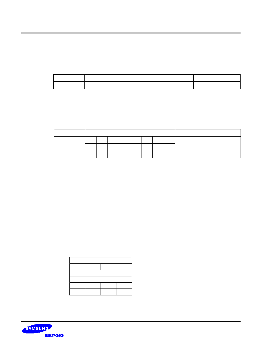
KS57C0502/C0504/P0504 MICROCONTROLLER
INSTRUCTION SET
545
CALL
Call Procedure
CALL
dst
Operation:
Operand
Operation Summary
Bytes
Cycles
ADR14
Call direct in page (14 bits)
3
4
Description:
CALL calls a subroutine located at the destination address. The instruction adds three to the
program counter to generate the return address and then pushes the result onto the stack,
decrementing the stack pointer by six. The EMB and ERB are also pushed to the stack. Program
execution continues with the instruction at this address. The subroutine may therefore begin
anywhere in the full 16-Kbyte program memory address space.
Operand
Binary Code
Operation Notation
ADR14
1
1
0
1
1
0
1
1
[(SP1) (SP2)]
EMB, ERB
0
1
a13 a12 a11
a10
a9
a8
[(SP3) (SP4)]
PC70
a7
a6
a5
a4
a3
a2
a1
a0
[(SP5) (SP6)]
PC138
Example:
The stack pointer value is 00H and the label 'PLAY' is assigned to program memory location
0E3FH. Executing the instruction
CALL
PLAY
at location 0123H generates the following values:
SP
=
0FAH
0FFH
=
0H
0FEH
=
EMB, ERB
0FDH
=
2H
0FCH
=
6H
0FBH
=
0H
0FAH
=
1H
PC
=
0E3FH
Data is written to stack locations 0FFH0FAH as follows:
0FAH
PC11 PC8
0FBH
0
0
PC13 PC12
0FCH
PC3 PC0
0FDH
PC7 PC4
0FEH
0
0
EMB
ERB
0FFH
0
0
0
0
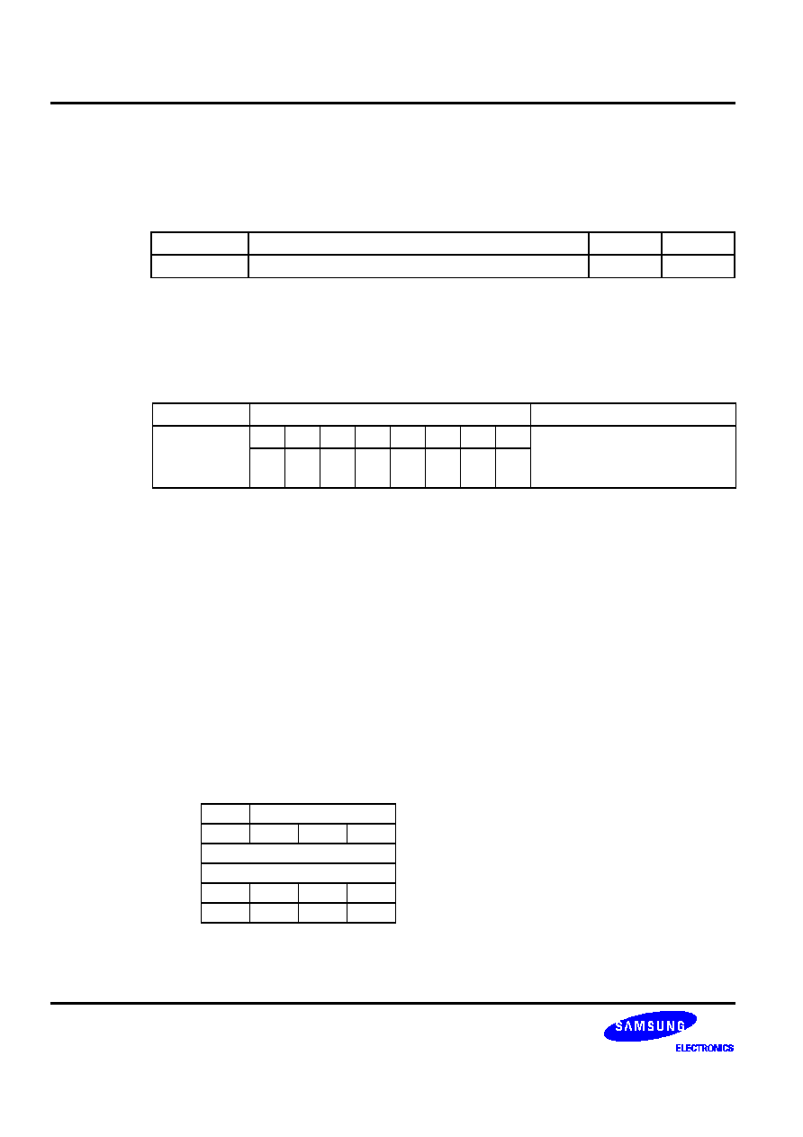
INSTRUCTION SET
KS57C0502/C0504/P0504 MICROCONTROLLER
546
CALLS
Call Procedure (Short)
CALLS
dst
Operation:
Operand
Operation Summary
Bytes
Cycles
ADR11
Call direct in page (11 bits)
2
3
Description:
The CALLS instruction unconditionally calls a subroutine located at the indicated address. The
instruction increments the PC twice to obtain the address of the following instruction. Then, it
pushes the result onto the stack, decrementing the stack pointer six times. The higher bits of the
PC, with the exception of the lower 11 bits, are cleared. The subroutine call must therefore be
located within the 2-Kbyte block (0000H07FFH) of program memory.
Operand
Binary Code
Operation Notation
ADR11
1
1
1
0
1
a10
a9
a8
[(SP1) (SP2)]
EMB, ERB
a7
a6
a5
a4
a3
a2
a1
a0
[(SP3) (SP4)]
PC70
[(SP5) (SP6)]
PC108
Example:
The stack pointer value is 00H and the label 'PLAY' is assigned to program memory location
0345H. Executing the instruction
CALLS
PLAY
at location 0123H will generate the following values:
SP
=
0FAH
0FFH
=
0H
0FEH
=
EMB, ERB
0FDH
=
2H
0FCH
=
5H
0FBH
=
0H
0FAH
=
1H
PC
=
0345H
Data is written to stack locations 0FFH0FAH as follows:
0FAH
0
PC10 PC8
0FBH
0
0
0
0
0FCH
PC3 PC0
0FDH
PC7 PC4
0FEH
0
0
EMB
ERB
0FFH
0
0
0
0

KS57C0502/C0504/P0504 MICROCONTROLLER
INSTRUCTION SET
547
CCF
Complement Carry Flag
CCF
Operation:
Operand
Operation Summary
Bytes
Cycles
--
Complement carry flag
1
1
Description:
The carry flag is complemented; if C = "1" it is changed to C = "0" and vice-versa.
Operand
Binary Code
Operation Notation
--
1
1
0
1
0
1
1
0
C
C
Example:
If the carry flag is logic zero, the instruction
CCF
changes the value to logic one.
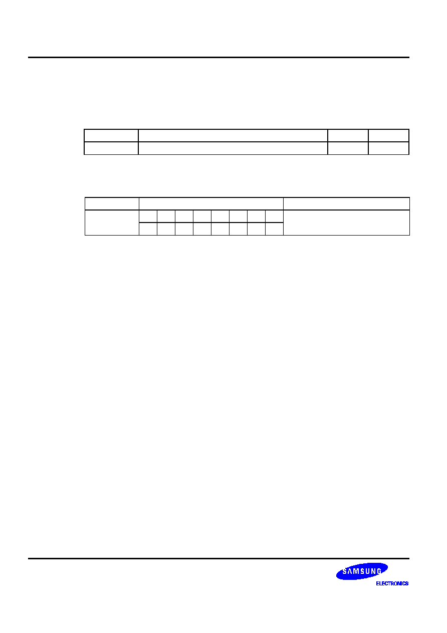
INSTRUCTION SET
KS57C0502/C0504/P0504 MICROCONTROLLER
548
COM
Complement Accumulator
COM
A
Operation:
Operand
Operation Summary
Bytes
Cycles
A
Complement accumulator (A)
2
2
Description:
The accumulator value is complemented; if the bit value of A is "1", it is changed to "0" and vice
versa.
Operand
Binary Code
Operation Notation
A
1
1
0
1
1
1
0
1
A
A
0
0
1
1
1
1
1
1
Example:
If the accumulator contains the value 4H (0100B), the instruction
COM
A
leaves the value 0BH (1011B) in the accumulator.
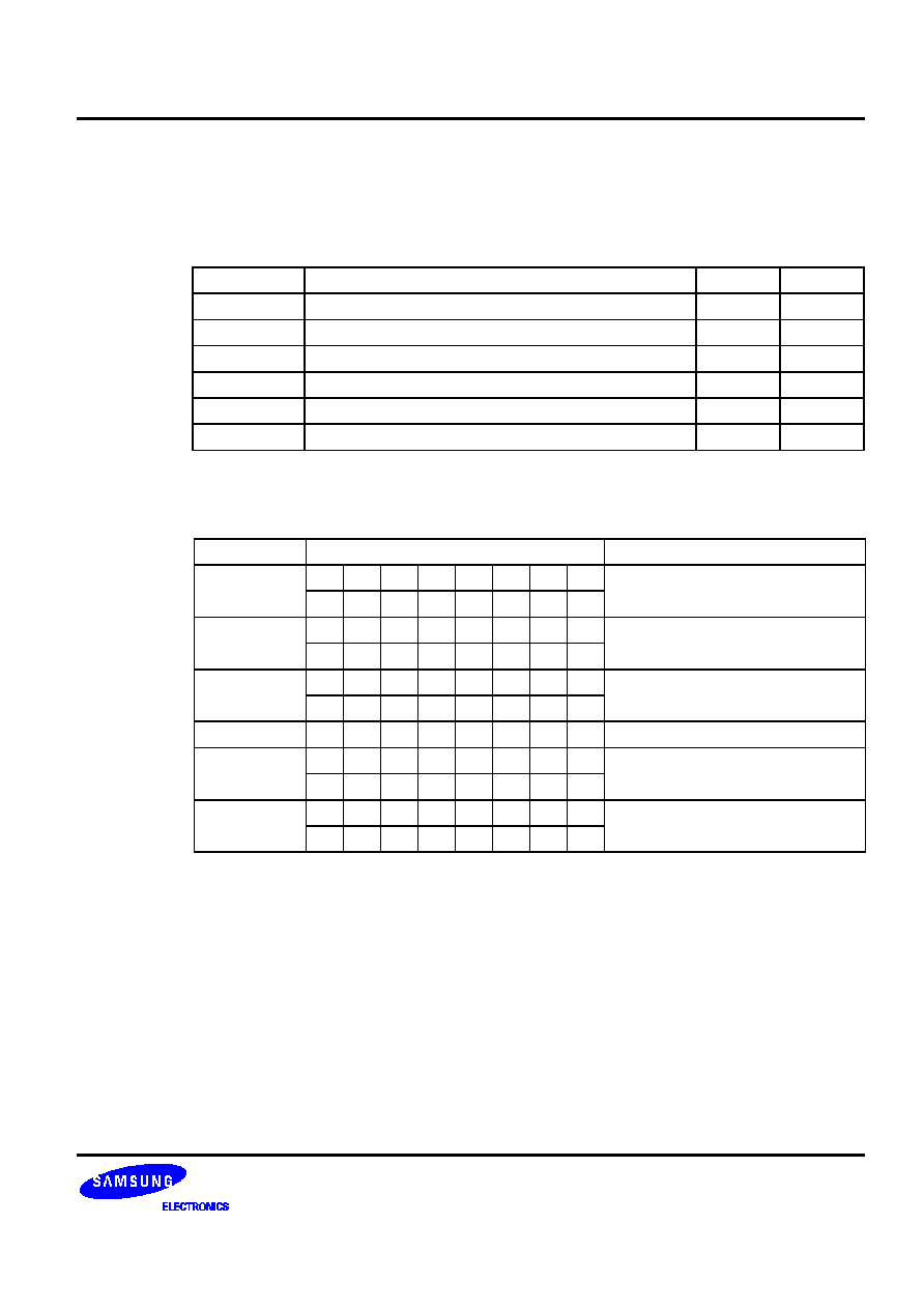
KS57C0502/C0504/P0504 MICROCONTROLLER
INSTRUCTION SET
549
CPSE
Compare and Skip if Equal
CPSE
dst,src
Operation:
Operand
Operation Summary
Bytes
Cycles
R,#im
Compare and skip if register equals #im
2
2 + S
@HL,#im
Compare and skip if indirect data memory equals #im
2
2 + S
A,R
Compare and skip if A equals R
2
2 + S
A,@HL
Compare and skip if A equals indirect data memory
1
1 + S
EA,@HL
Compare and skip if EA equals indirect data memory
2
2 + S
EA,RR
Compare and skip if EA equals RR
2
2 + S
Description:
CPSE compares the source operand (subtracts it from) the destination operand, and skips the
next instruction if the values are equal. Neither operand is affected by the comparison.
Operand
Binary Code
Operation Notation
R,#im
1
1
0
1
1
0
0
1
Skip if R = im
d3
d2
d1
d0
0
r2
r1
r0
@HL,#im
1
1
0
1
1
1
0
1
Skip if (HL) = im
0
1
1
1
d3
d2
d1
d0
A,R
1
1
0
1
1
1
0
1
Skip if A = R
0
1
1
0
1
r2
r1
r0
A,@HL
0
0
1
1
1
0
0
0
Skip if A = (HL)
EA,@HL
1
1
0
1
1
1
0
0
Skip if A = (HL), E = (HL+1)
0
0
0
0
1
0
0
1
EA,RR
1
1
0
1
1
1
0
0
Skip if EA = RR
1
1
1
0
1
r2
r1
0
Example:
The extended accumulator contains the value 34H and register pair HL contains 56H. The
second instruction (RET) in the instruction sequence
CPSE
EA,HL
RET
is not skipped. That is, the subroutine returns because the result of the comparison is 'not equal.'

INSTRUCTION SET
KS57C0502/C0504/P0504 MICROCONTROLLER
550
DECS
Decrement and Skip on Borrow
DECS
dst
Operation:
Operand
Operation Summary
Bytes
Cycles
R
Decrement register (R); skip on borrow
1
1 + S
RR
Decrement register pair (RR); skip on borrow
2
2 + S
Description:
The destination is decremented by one. An original value of 00H will underflow to 0FFH. If a
borrow occurs, a skip is executed. The carry flag value is unaffected.
Operand
Binary Code
Operation Notation
R
0
1
0
0
1
r2
r1
r0
R
R1; skip on borrow
RR
1
1
0
1
1
1
0
0
RR
RR1; skip on borrow
1
1
0
1
1
r2
r1
0
Examples:
1.
Register pair HL contains the value 7FH (01111111B). The following instruction leaves the
value 7EH in register pair HL:
DECS
HL
2.
Register A contains the value 0H. The following instruction sequence leaves the value 0FFH
in register A. Because a "borrow" occurs, the 'CALL PLAY1' instruction is skipped and the
'CALL PLAY2' instruction is executed:
DECS
A
; "Borrow" occurs
CALL
PLAY1
; Skipped
CALL
PLAY2
; Executed
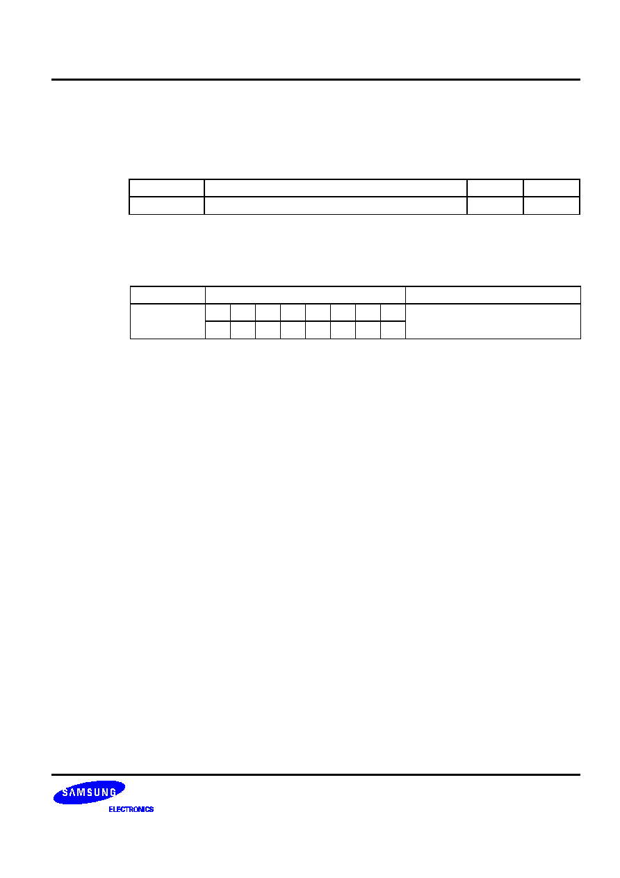
KS57C0502/C0504/P0504 MICROCONTROLLER
INSTRUCTION SET
551
DI
Disable Interrupts
DI
Operation:
Operand
Operation Summary
Bytes
Cycles
--
Disable all interrupts
2
2
Description:
Bit 3 of the interrupt priority register IPR, IME, is cleared to logic zero, disabling all interrupts.
Interrupts can still set their respective interrupt status latches, but the CPU will not directly
service them.
Operand
Binary Code
Operation Notation
--
1
1
1
1
1
1
1
0
IME
0
1
0
1
1
0
0
1
0
Example:
If the IME bit (bit 3 of the IPR) is logic one (e.g., all instructions are enabled), the instruction
DI
sets the IME bit to logic zero, disabling all interrupts.

INSTRUCTION SET
KS57C0502/C0504/P0504 MICROCONTROLLER
552
EI
Enable Interrupts
EI
Operation:
Operand
Operation Summary
Bytes
Cycles
--
Enable all interrupts
2
2
Description:
Bit 3 of the interrupt priority register IPR (IME) is set to logic one. This allows all interrupts to be
serviced when they occur, assuming they are enabled. If an interrupt's status latch was
previously enabled by an interrupt, this interrupt can also be serviced.
Operand
Binary Code
Operation Notation
--
1
1
1
1
1
1
1
1
IME
1
1
0
1
1
0
0
1
0
Example:
If the IME bit (bit 3 of the IPR) is logic zero (e.g., all instructions are disabled), the instruction
EI
sets the IME bit to logic one, enabling all interrupts.

KS57C0502/C0504/P0504 MICROCONTROLLER
INSTRUCTION SET
553
IDLE
Idle Operation
IDLE
Operation:
Operand
Operation Summary
Bytes
Cycles
--
Engage CPU idle mode
2
2
Description:
IDLE causes the CPU clock to stop while the system clock continues oscillating by setting bit 2 of
the power control register (PCON). After an IDLE instruction has been executed, peripheral
hardware remains operative.
In application programs, an IDLE instruction should be immediately followed by at least three
NOP instructions. This ensures an adequate time interval for the clock to stabilize before the
next instruction is executed.
Operand
Binary Code
Operation Notation
--
1
1
1
1
1
1
1
1
PCON.2
1
1
0
1
0
0
0
1
1
Example:
The instruction sequence
IDLE
NOP
NOP
NOP
sets bit 2 of the PCON register to logic one, stopping the CPU clock. The three NOP instructions
provide the necessary timing delay for clock stabilization before the next instruction in the
program sequence is executed.
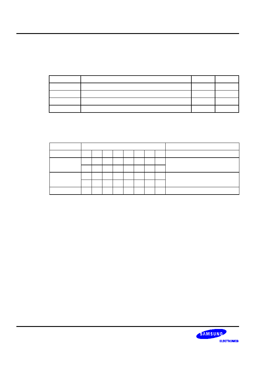
INSTRUCTION SET
KS57C0502/C0504/P0504 MICROCONTROLLER
554
INCS
Increment and Skip on Carry
INCS
dst
Operation:
Operand
Operation Summary
Bytes
Cycles
R
Increment register (R); skip on carry
1
1 + S
DA
Increment direct data memory; skip on carry
2
2 + S
@HL
Increment indirect data memory; skip on carry
2
2 + S
RRb
Increment register pair (RRb); skip on carry
1
1 + S
Description:
The instruction INCS increments the value of the destination operand by one. An original value
of 0FH will, for example, overflow to 00H. If a carry occurs, the next instruction is skipped. The
carry flag value is unaffected.
Operand
Binary Code
Operation Notation
R
0
1
0
1
1
r2
r1
r0
R
R + 1; skip on carry
DA
1
1
0
0
1
0
1
0
DA
DA + 1; skip on carry
a7
a6
a5
a4
a3
a2
a1
a0
@HL
1
1
0
1
1
1
0
1
(HL)
(HL) + 1; skip on carry
0
1
1
0
0
0
1
0
RRb
1
0
0
0
0
r2
r1
0
RRb
RRb + 1; skip on carry
Example:
Register pair HL contains the value 7EH (01111110B). RAM location 7EH contains 0FH. The
instruction sequence
INCS
@HL
; 7EH
"0"
INCS
HL
; Skip
INCS
@HL
; 7EH
"1"
leaves the register pair HL with the value 7EH and RAM location 7EH with the value 1H.
Because a carry occurred, the second instruction is skipped. The carry flag value remains
unchanged.
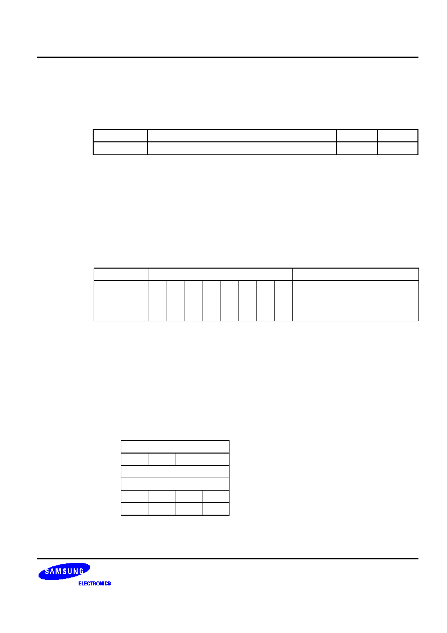
KS57C0502/C0504/P0504 MICROCONTROLLER
INSTRUCTION SET
555
IRET
Return from Interrupt
IRET
Operation:
Operand
Operation Summary
Bytes
Cycles
--
Return from interrupt
1
3
Description:
IRET is used at the end of an interrupt service routine. It pops the PC values successively from
the stack and restores them to the program counter. The stack pointer is incremented by six and
the PSW, enable memory bank (EMB) bit, and enable register bank (ERB) bit are also
automatically restored to their pre-interrupt values. Program execution continues from the
resulting address, which is generally the instruction immediately after the point at which the
interrupt request was detected. If a lower-level or same-level interrupt was pending when the
IRET was executed, IRET will be executed before the pending interrupt is processed.
Because the 'a14' bit of an interrupt return address is not stored in the stack, this bit location is
always interpreted as a logic zero. The start address in the ROM must for this reason be 3FFFH.
Operand
Binary Code
Operation Notation
--
1
1
0
1
0
1
0
1
PC138
(SP + 1) (SP)
PC70
(SP + 2) (SP + 3)
PSW
(SP + 4) (SP + 5)
SP
SP + 6
Example:
The stack pointer contains the value 0FAH. An interrupt is detected in the instruction at location
0122H. RAM locations 0FDH, 0FCH, and 0FAH contain the values 2H, 3H, and 1H, respectively.
The instruction
IRET
leaves the stack pointer with the value 00H and the program returns to continue execution at
location 123H.
During a return from interrupt, data is popped from the stack to the program counter. The data in
stack locations 0FFH0FAH is organized as follows:
0FAH
PC11 PC8
0FBH
0
0
PC13 PC12
0FCH
PC3 PC0
0FDH
PC7 PC4
0FEH
IS1
IS0
EMB
ERB
0FFH
C
SC2
SC1
SC0

INSTRUCTION SET
KS57C0502/C0504/P0504 MICROCONTROLLER
556
JP
Jump
JP
dst
Operation:
Operand
Operation Summary
Bytes
Cycles
ADR14
Jump to direct address (14 bits)
3
3
Description:
JP causes an unconditional branch to the indicated address by replacing the contents of the
program counter with the address specified in the destination operand. The destination can be
anywhere in the 16-Kbyte program memory address space.
Operand
Binary Code
Operation Notation
ADR14
1
1
0
1
1
0
1
1
PC130
ADR14
0
0
a13 a12 a11
a10
a9
a8
a7
a6
a5
a4
a3
a2
a1
a0
Example:
The label 'SYSCON' is assigned to the instruction at program location 07FFH. The instruction
JP
SYSCON
at location 0123H loads the program counter with the value 07FFH.
KS57C0502/C0504/P0504 MICROCONTROLLER
INSTRUCTION SET
557
JPS
Jump (Short)
JPS
dst
Operation:
Operand
Operation Summary
Bytes
Cycles
ADR12
Jump direct in page (12 bits)
2
2
Description:
JPS causes an unconditional branch to the indicated address within the 4-Kbyte program
memory address space. Bits 011 of the program counter are replaced with the directly specified
address. The destination address for this jump is specified to the assembler by a label or by an
actual address in program memory.
Operand
Binary Code
Operation Notation
ADR12
1
0
0
1
a11
a10
a9
a8
PC130
PC1312 + ADR11
0
a7
a6
a5
a4
a3
a2
a1
a0
Example:
The label 'SUB' is assigned to the instruction at program memory location 00FFH. The
instruction
JPS
SUB
at location 0EABH will load the program counter with the value 00FFH. Normally, the JPS
instruction jumps to the address in the block in which the instruction is located. If the first byte of
the instruction code is located at address xFFEH or xFFFH, the instruction will jump to the next
block. If the instruction 'JPS SUB' were located instead at program memory address 0FFEH or
0FFFH, the instruction 'JPS SUB' would load the PC with the value 10FFH, causing a program
malfunction.
INSTRUCTION SET
KS57C0502/C0504/P0504 MICROCONTROLLER
558
JR
Jump Relative (Very Short)
JR
dst
Operation:
Operand
Operation Summary
Bytes
Cycles
#im
Branch to relative immediate address
1
2
@WX
Branch relative to contents of WX register
2
3
@EA
Branch relative to contents of EA
2
3
Description:
JR causes the relative address to be added to the program counter and passes control to the
instruction whose address is now in the PC. The range of the relative address is current PC 15
to current PC + 16. The destination address for this jump is specified to the assembler by a label,
an actual address, or by immediate data using a plus sign (+) or a minus sign ().
For immediate addressing, the (+) range is from 2 to 16 and the () range is from 1 to 15. If
a 0, 1, or any other number that is outside these ranges are used, the assembler interprets it as
an error.
For JR @WX and JR @EA branch relative instructions, the valid range for the relative address is
0H0FFH. The destination address for these jumps can be specified to the assembler by a label
that lies anywhere within the current 256-byte block.
Normally, the 'JR @WX' and 'JR @EA' instructions jump to the address in the page in which
the instruction is located. However, if the first byte of the instruction code is located at address
xxFEH or xxFFH, the instruction will jump to the next page.
Operand
Binary Code
Operation Notation
#im
*
PC130
ADR (PC15 to
PC+16)
@WX
1
1
0
1
1
1
0
1
PC130
PC138 + (WX)
0
1
1
0
0
1
0
0
@EA
1
1
0
1
1
1
0
1
PC130
PC138 + (EA)
0
1
1
0
0
0
0
0
First Byte
Condition
*
JR #im
0
0
0
1
a3
a2
a1
a0
PC
PC+2 to PC+16
0
0
0
0
a3
a2
a1
a0
PC
PC1 to PC15

KS57C0502/C0504/P0504 MICROCONTROLLER
INSTRUCTION SET
559
JR
Jump Relative (Very Short)
JR
(Continued)
Examples:
1.
A short form for a relative jump to label 'KK' is the instruction
JR KK
where 'KK' must be within the allowed range of current PC15 to current PC+16. The JR
instruction has in this case the effect of an unconditional JP instruction.
2.
In the following instruction sequence, if the instruction 'LD WX, #02H' were to be executed in
place of 'LD WX,#00H', the program would jump to 1002H and 'JPS BBB' would be
executed. If 'LD EA,#04H' were to be executed, the jump would be to1004H and 'JPS CCC'
would be executed.
ORG
1000H
JPS
AAA
JPS
BBB
JPS
CCC
JPS
DDD
LD
WX,#00H
; WX
00H
LD
EA,WX
ADS
WX,EA
; WX
(WX) + (WX)
JR
@WX
; Current PC138 (10H) + WX (00H) = 1000H
; Jump to address 1000H and execute JPS AAA
3.
Here is another example:
ORG
1100H
LD
A,#0H
LD
A,#1H
LD
A,#2H
LD
A,#3H
LD
30H,A
; Address 30H
A
JPS
YYY
XXX
LD
EA,#00H
; EA
00H
JR
@EA
; Jump to address 1100H
; Address 30H
00H
If 'LD EA,#01H' were to be executed in place of 'LD EA,#00H', the program would jump to
1001H and address 30H would contain the value 1H. If 'LD EA,#02H' were to be executed,
the jump would be to 1002H and address 30H would contain the value 2H.
INSTRUCTION SET
KS57C0502/C0504/P0504 MICROCONTROLLER
560
LD
Load
LD
dst,src
Operation:
Operand
Operation Summary
Bytes
Cycles
A,#im
Load 4-bit immediate data to A
1
1
A,@RRa
Load indirect data memory contents to A
1
1
A,DA
Load direct data memory contents to A
2
2
A,Ra
Load register contents to A
2
2
Ra,#im
Load 4-bit immediate data to register
2
2
RR,#imm
Load 8-bit immediate data to register
2
2
DA,A
Load contents of A to direct data memory
2
2
Ra,A
Load contents of A to register
2
2
EA,@HL
Load indirect data memory contents to EA
2
2
EA,DA
Load direct data memory contents to EA
2
2
EA,RRb
Load register contents to EA
2
2
@HL,A
Load contents of A to indirect data memory
1
1
DA,EA
Load contents of EA to data memory
2
2
RRb,EA
Load contents of EA to register
2
2
@HL,EA
Load contents of EA to indirect data memory
2
2
Description:
The contents of the source are loaded into the destination. The source's contents are
unaffected.If an instruction such as 'LD A,#im' (LD EA,#imm) or 'LD HL,#imm' is written more
than two times in succession, only the first LD will be executed; the other similar instructions that
immediately follow the first LD will be treated like a NOP. This is called the 'redundancy effect'
(see examples below).
Operand
Binary Code
Operation Notation
A,#im
1
0
1
1
d3
d2
d1
d0
A
im
A,@RRa
1
0
0
0
1
i2
i1
i0
A
(RRa)
A,DA
1
0
0
0
1
1
0
0
A
DA
a7
a6
a5
a4
a3
a2
a1
a0
A,Ra
1
1
0
1
1
1
0
1
A
Ra
0
0
0
0
1
r2
r1
r0
Ra,#im
1
1
0
1
1
0
0
1
Ra
im
d3
d2
d1
d0
1
r2
r1
r0
KS57C0502/C0504/P0504 MICROCONTROLLER
INSTRUCTION SET
561
LD
Load
LD
(Continued)
Description:
Operand
Binary Code
Operation Notation
RR,#imm
1
0
0
0
0
r2
r1
1
RR
imm
d7
d6
d5
d4
d3
d2
d1
d0
DA,A
1
0
0
0
1
0
0
1
DA
A
a7
a6
a5
a4
a3
a2
a1
a0
Ra,A
1
1
0
1
1
1
0
1
Ra
A
0
0
0
0
0
r2
r1
r0
EA,@HL
1
1
0
1
1
1
0
0
A
(HL), E
(HL + 1)
0
0
0
0
1
0
0
0
EA,DA
1
1
0
0
1
1
1
0
A
DA, E
DA + 1
a7
a6
a5
a4
a3
a2
a1
a0
EA,RRb
1
1
0
1
1
1
0
0
EA
RRb
1
1
1
1
1
r2
r1
0
@HL,A
1
1
0
0
0
1
0
0
(HL)
A
DA,EA
1
1
0
0
1
1
0
1
DA
A, DA + 1
E
a7
a6
a5
a4
a3
a2
a1
a0
RRb,EA
1
1
0
1
1
1
0
0
RRb
EA
1
1
1
1
0
r2
r1
0
@HL,EA
1
1
0
1
1
1
0
0
(HL)
A, (HL + 1)
E
0
0
0
0
0
0
0
0
Examples:
1.
RAM location 30H contains the value 4H. The RAM location values are 40H, 41H and 0AH,
3H respectively. The following instruction sequence leaves the value 40H in point pair HL,
0AH in the accumulator and in RAM location 40H, and 3H in register E.
LD
HL,#30H
; HL
30H
LD
A,@HL
; A
4H
LD
HL,#40H
; HL
40H
LD
EA,@HL
; A
0AH, E
3H
LD
@HL,A
; RAM (40H)
0AH

INSTRUCTION SET
KS57C0502/C0504/P0504 MICROCONTROLLER
562
LD
Load
LD
(Continued)
Examples:
2.
If an instruction such as LD A,#im (LD EA,#imm) or LD HL,#imm is written more than two
times in succession, only the first LD is executed; the next instructions are treated as NOPs.
Here are two examples of this 'redundancy effect':
LD
A,#1H
; A
1H
LD
EA,#2H
; NOP
LD
A,#3H
; NOP
LD
23H,A
; (23H)
1H
LD
HL,#10H
; HL
10H
LD
HL,#20H
; NOP
LD
A,#3H
; A
3H
LD
EA,#35
; NOP
LD
@HL,A
; (10H)
3H
The following table contains descriptions of special characteristics of the LD instruction when
used in different addressing modes:
Instruction
Operation Description and Guidelines
LD A,#im
Because the 'redundancy effect' occurs with instructions like LD EA,#imm, if
this instruction is used consecutively, the second and additional instructions of
the same type will be treated like NOPs.
LD A,@RRa
Load the data memory contents pointed to by 8-bit RRa register pairs (HL, WX,
WL) to the A register.
LD A,DA
Load direct data memory contents to the A register.
LD A,Ra
Load 4-bit register Ra (E, L, H, X, W, Z, Y) to the A register.
LD Ra,#im
Load 4-bit immediate data into the Ra register (E, L, H, X, W, Y, Z).
LD RR,#imm
Load 8-bit immediate data into the Ra register (EA, HL, WX, YZ). There is a
redundancy effect if the operation addresses the HL or EA registers.
LD DA,A
Load contents of register A to direct data memory address.
LD Ra,A
Load contents of register A to 4-bit Ra register (E, L, H, X, W, Z, Y).

KS57C0502/C0504/P0504 MICROCONTROLLER
INSTRUCTION SET
563
LD
Load
LD
(Concluded)
Examples:
Instruction
Operation Description and Guidelines
LD EA,@HL
Load data memory contents pointed to by 8-bit register HL to the A register,
and the contents of HL+1 to the E register. The contents of register L must be
an even number. If the number is odd, the LSB of register L is recognized as a
logic zero (an even number), and it is not replaced with the true value. For
example, 'LD HL,#36H' loads immediate 36H to HL and the next instruction
'LD EA,@HL' loads the contents of 36H to register A and the contents of 37H
to register E.
LD EA,DA
Load direct data memory contents of DA to the A register, and the next direct
data memory contents of DA + 1 to the E register. The DA value must be an
even number. If it is an odd number, the LSB of DA is recognized as a logic
zero (an even number), and it is not replaced with the true value. For example,
'LD EA,37H' loads the contents of 36H to the A register and the contents of
37H to the E register.
LD EA,RRb
Load 8-bit RRb register (HL, WX, YZ) to the EA register. H, W, and Y register
values are loaded into the E register, and the L, X, and Z values into the A
register.
LD @HL,A
Load A register contents to data memory location pointed to by the 8-bit HL
register value.
LD DA,EA
Load the A register contents to direct data memory and the E register contents
to the next direct data memory location. The DA value must be an even
number. If it is an odd number, the LSB of the DA value is recognized as logic
zero (an even number), and is not replaced with the true value.
LD RRb,EA
Load contents of EA to the 8-bit RRb register (HL, WX, YZ). The E register is
loaded into the H, W, and Y register and the A register into the L, X, and Z
register.
LD @HL,EA
Load the A register to data memory location pointed to by the 8-bit HL register,
and the E register contents to the next location, HL + 1. The contents of the L
register must be an even number. If the number is odd, the LSB of the L
register is recognized as logic zero (an even number), and is not replaced with
the true value. For example, 'LD HL,#36H' loads immediate 36H to register
HL; the instruction 'LD @HL,EA' loads the contents of A into address 36H and
the contents of E into address 37H.
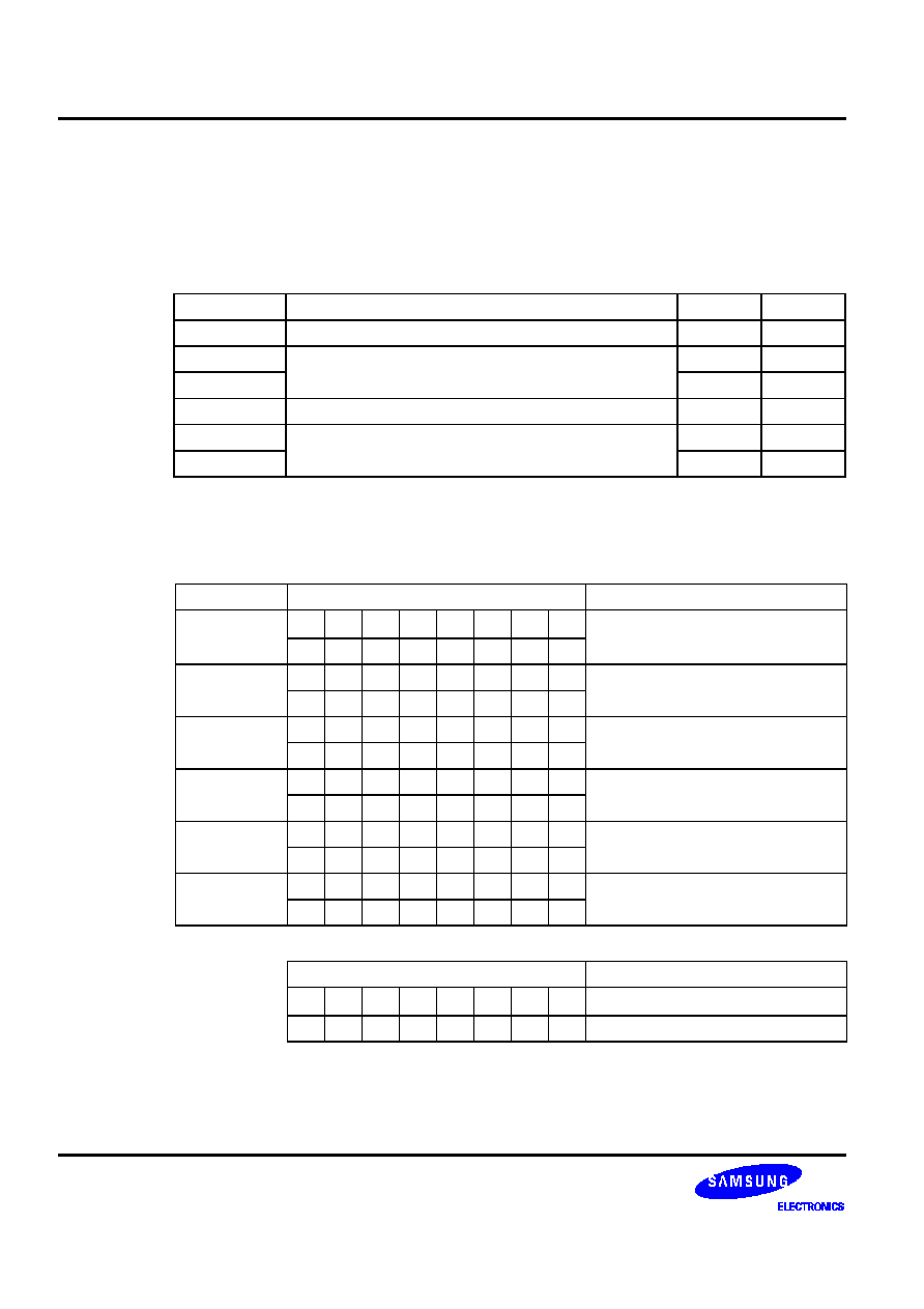
INSTRUCTION SET
KS57C0502/C0504/P0504 MICROCONTROLLER
564
LDB
Load Bit
LDB
dst,src.b
LDB
dst.b,src
Operation:
Operand
Operation Summary
Bytes
Cycles
mema.b,C
Load carry bit to a specified memory bit
2
2
memb.@L,C
Load carry bit to a specified indirect memory bit
2
2
@H+DA.b,C
2
2
C,mema.b
Load memory bit to a specified carry bit
2
2
C,memb.@L
Load indirect memory bit to a specified carry bit
2
2
C,@H+DA.b
2
2
Description:
The Boolean variable indicated by the first or second operand is copied into the location
specified by the second or first operand. One of the operands must be the carry flag; the other
can be any directly or indirectly addressable bit. The source is unaffected.
Operand
Binary Code
Operation Notation
mema.b,C
*
1
1
1
1
1
1
0
0
mema.b
C
memb.@L,C
1
1
1
1
1
1
0
0
memb.72 + [L.32]. [L.10]
C
0
1
0
0
a5
a4
a3
a2
@H+DA.b,C
1
1
1
1
1
1
0
0
H + [DA.30].b
(C)
0
b2
b1
b0
a3
a2
a1
a0
C,mema.b*
1
1
1
1
0
1
0
0
C
mema.b
C,memb.@L
1
1
1
1
0
1
0
0
C
memb.72 + [L.32] . [L.10]
0
1
0
0
a5
a4
a3
a2
C,@H+DA.b
1
1
1
1
0
1
0
0
C
[H + DA.30].b
0
b2
b1
b0
a3
a2
a1
a0
Second Byte
Bit Addresses
*
mema.b
1
0
b1
b0
a3
a2
a1
a0
FB0HFBFH
1
1
b1
b0
a3
a2
a1
a0
FF0HFFFH

KS57C0502/C0504/P0504 MICROCONTROLLER
INSTRUCTION SET
565
LDB
Load Bit
LDB
(Continued)
Examples:
1.
The carry flag is set and the data value at input pin P1.0 is logic zero. The following
instruction clears the carry flag to logic zero.
LDB
C,P1.0
2.
The P1 address is FF1H and the L register contains the value 9H (1001B). The address
(memb.72) is 111100B and (L.32) is 10B. The resulting address is 11110010B or FF2H
and P2 is addressed. The bit value (L.10) is specified as 01B (bit 1).
LD
L,#9H
LDB
C,P1.@L
; P1.@L specifies P2.1 and C
P2.1
3.
The H register contains the value 2H and FLAG = 20H.3. The address for H is 0010B and for
FLAG(30) the address is 0000B. The resulting address is 00100000B or 20H. The bit value
is 3. Therefore, @H+FLAG = 20H.3.
FLAG
EQU
20H.3
LD
H,#2H
LDB
C,@H+FLAG ;
C
FLAG (20H.3)
4.
The following instruction sequence sets the carry flag and the loads the "1" data value to the
output pin P2.0, setting it to output mode:
SCF
;
C
"1"
LDB
P2.0,C
;
P2.0
"1"
5.
The P1 address is FF1H and L = 9H (1001B). The address (memb.72) is 111100B and
(L.32) is 10B. The resulting address, 11110010B specifies P2. The bit value (L.10) is
specified as 01B (bit 1). Therefore, P1.@L = P2.1.
SCF
;
C
"1"
LD
L,#9H
LDB
P1.@L,C
;
P1.@L specifies P2.1
;
P2.1
"1"
6.
In this example, H = 2H and FLAG = 20H.3 and the address 20H is specified. Because the
bit value is 3, @H+FLAG = 20H.3:
FLAG
EQU 20H.3
RCF
;
C
"0"
LD
H,#2H
LDB@H+FLAG,C
;
FLAG(20H.3)
"0"
NOTE
Port pin names used in examples 4 and 5 may vary with different SAM47 devices.

INSTRUCTION SET
KS57C0502/C0504/P0504 MICROCONTROLLER
566
LDC
Load Code Byte
LDC
dst,src
Operation:
Operand
Operation Summary
Bytes
Cycles
EA,@WX
Load code byte from WX to EA
1
3
EA,@EA
Load code byte from EA to EA
1
3
Description:
This instruction is used to load a byte from program memory into an extended accumulator. The
address of the byte fetched is the five highest bit values in the program counter and the contents
of an 8-bit working register (either WX or EA). The contents of the source are unaffected.
Operand
Binary Code
Operation Notation
EA,@WX
1
1
0
0
1
1
0
0
EA
[PC138 + (WX)]
EA,@EA
1
1
0
0
1
0
0
0
EA
[PC138 + (EA)]
Examples:
1.
The following instructions will load one of four values defined by the define byte (DB)
directive
to the extended accumulator:
LD
EA,#00H
CALL
DISPLAY
JPS
MAIN
ORG
0500H
DB
66H
DB
77H
DB
88H
DB
99H
·
·
·
DISPLAY LDC
EA,@EA
; EA
address 0500H = 66H
RET
If the instruction 'LD EA,#01H' is executed in place of 'LD EA,#00H', The content of 0501H
(77H) is loaded to the EA register. If 'LD EA,#02H' is executed, the content of address
0502H (88H) is loaded to EA.

KS57C0502/C0504/P0504 MICROCONTROLLER
INSTRUCTION SET
567
LDC
Load Code Byte
LDC
(Continued)
Examples:
2.
The following instructions will load one of four values defined by the define byte (DB)
directive
to the extended accumulator:
ORG
0500
DB
66H
DB
77H
DB
88H
DB
99H
·
·
·
DISPLAY LD
WX,#00H
LDC
EA,@WX
; EA
address 0500H = 66H
RET
If the instruction 'LD WX,#01H' is executed in place of 'LD WX,#00H', then
EA
address 0501H = 77H.
If the instruction 'LD WX,#02H' is executed in place of 'LD WX,#00H', then
EA
address 0502H = 88H.
3.
Normally, the LDC EA, @EA and the LDC EA, @WX instructions reference the table data
on the page on which the instruction is located. If, however, the instruction is located at
address xxFFH, it will reference table data on the next page. In this example, the upper 4
bits of the address at location 0200H is loaded into register E and the lower 4 bits into
register A:
ORG
01FDH
01FDH
LD
WX,#00H
01FFH
LDC
EA,@WX
; E
upper 4 bits of 0200H address
; A
lower 4 bits of 0200H address
4.
Here is another example of page referencing with the LDC instruction:
ORG
0100
DB
67H
SMB
0
LD
HL,#30H
; Even number
LD
WX,#00H
LDC
EA,@WX
; E
upper 4 bits of 0100H address
; A
lower 4 bits of 0100H address
LD
@HL,EA
; RAM (30H)
7, RAM (31H)
6

INSTRUCTION SET
KS57C0502/C0504/P0504 MICROCONTROLLER
568
LDD
Load Data Memory and Decrement
LDD
dst
Operation:
Operand
Operation Summary
Bytes
Cycles
A,@HL
Load indirect data memory contents to A; decrement
register L contents and skip on borrow
1
2 + S
Description:
The contents of a data memory location are loaded into the accumulator, and the contents of the
register L are decremented by one. If a "borrow" occurs (e.g., if the resulting value in register L is
0FH), the next instruction is skipped. The contents of data memory and the carry flag value are
not affected.
Operand
Binary Code
Operation Notation
A,@HL
1
0
0
0
1
0
1
1
A
(HL), then L
L1;
skip if L = 0FH
Example:
In this example, assume that register pair HL contains 20H and internal RAM location 20H
contains the value 0FH:
LD
HL,#20H
LDD
A,@HL
; A
(HL) and L
L1
JPS
XXX
; Skip
JPS
YYY
; H
2H and L
0FH
The instruction 'JPS XXX' is skipped because a "borrow" occurred after the 'LDD A,@HL' and
instruction 'JPS YYY' is executed.

KS57C0502/C0504/P0504 MICROCONTROLLER
INSTRUCTION SET
569
LDI
Load Data Memory and Increment
LDI
dst,src
Operation:
Operand
Operation Summary
Bytes
Cycles
A,@HL
Load indirect data memory to A; increment register L
contents and skip on overflow
1
2 + S
Description:
The contents of a data memory location are loaded into the accumulator, and the contents of the
register L are incremented by one. If an overflow occurs (e.g., if the resulting value in register L
is 0H), the next instruction is skipped. The contents of data memory and the carry flag value are
not affected.
Operand
Binary Code
Operation Notation
A,@HL
1
0
0
0
1
0
1
0
A
(HL), then L
L+1;
skip if L = 0H
Example:
Assume that register pair HL contains the address 2FH and internal RAM location 2FH contains
the value 0FH:
LD
HL,#2FH
LDI
A,@HL
; A
(HL) and L
L+1
JPS
XXX
; Skip
JPS
YYY
; H
2H and L
0H
The instruction 'JPS XXX' is skipped because an overflow occurred after the 'LDI A,@HL' and
the instruction 'JPS YYY' is executed.
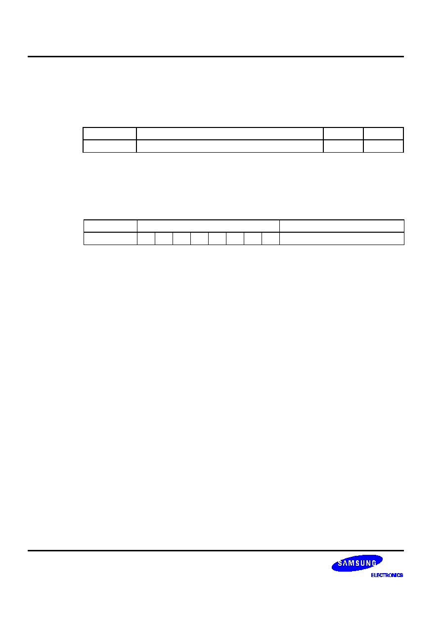
INSTRUCTION SET
KS57C0502/C0504/P0504 MICROCONTROLLER
570
NOP
No Operation
NOP
Operation:
Operand
Operation Summary
Bytes
Cycles
--
No operation
1
1
Description:
No operation is performed by a NOP instruction. It is typically used for timing delays.
One NOP causes a 1-cycle delay: with a 1-µs cycle time, five NOPs would therefore cause a 5-
µs delay. Program execution continues with the instruction immediately following the NOP. Only
the PC is affected. At least three NOP instructions should follow a STOP or IDLE instruction.
Operand
Binary Code
Operation Notation
--
1
0
1
0
0
0
0
0
No operation
Example:
Three NOP instructions follow the STOP instruction to provide a short interval for clock
stabilization before power-down mode is initiated:
STOP
NOP
NOP
NOP
KS57C0502/C0504/P0504 MICROCONTROLLER
INSTRUCTION SET
571
OR
Logical OR
OR
dst,src
Operation:
Operand
Operation Summary
Bytes
Cycles
A, #im
Logical-OR immediate data to A
2
2
A, @HL
Logical-OR indirect data memory contents to A
1
1
EA,RR
Logical-OR double register to EA
2
2
RRb,EA
Logical-OR EA to double register
2
2
Description:
The source operand is logically ORed with the destination operand. The result is stored in the
destination. The contents of the source are unaffected.
Operand
Binary Code
Operation Notation
A, #im
1
1
0
1
1
1
0
1
A
A OR im
0
0
1
0
d3
d2
d1
d0
A, @HL
0
0
1
1
1
0
1
0
A
A OR (HL)
EA,RR
1
1
0
1
1
1
0
0
EA
EA OR RR
0
0
1
0
1
r2
r1
0
RRb,EA
1
1
0
1
1
1
0
0
RRb
RRb OR EA
0
0
1
0
0
r2
r1
0
Example:
If the accumulator contains the value 0C3H (11000011B) and register pair HL the value 55H
(01010101B), the instruction
OR
EA,@HL
leaves the value 0D7H (11010111B) in the accumulator .

INSTRUCTION SET
KS57C0502/C0504/P0504 MICROCONTROLLER
572
POP
Pop from Stack
POP
dst
Operation:
Operand
Operation Summary
Bytes
Cycles
RR
Pop to register pair from stack
1
1
SB
Pop SMB and SRB values from stack
2
2
Description:
The contents of the RAM location addressed by the stack pointer is read, and the SP is
incremented by two. The value read is then transferred to the variable indicated by the
destination operand.
Operand
Binary Code
Operation Notation
RR
0
0
1
0
1
r2
r1
0
RR
L
(SP), RR
H
(SP+1)
SP
SP+2
SB
1
1
0
1
1
1
0
1
(SRB)
(SP), SMB
(SP+1),
SP
SP+2
0
1
1
0
0
1
1
0
Example:
The SP value is equal to 0EDH, and RAM locations 0EFH through 0EDH contain the values 2H,
3H, and 4H, respectively. The instruction
POP
HL
leaves the stack pointer set to 0EFH and the data pointer pair HL set to 34H.
KS57C0502/C0504/P0504 MICROCONTROLLER
INSTRUCTION SET
573
PUSH
Push onto Stack
PUSH
src
Operation:
Operand
Operation Summary
Bytes
Cycles
RR
Push register pair onto stack
1
1
SB
Push SMB and SRB values onto stack
2
2
Description:
The SP is then decremented by two and the contents of the source operand are copied into the
RAM location addressed by the stack pointer, thereby adding a new element to the top of the
stack.
Operand
Binary Code
Operation Notation
RR
0
0
1
0
1
r2
r1
1
(SP1)
RR
H
, (SP2)
RR
L
SP
SP2
SB
1
1
0
1
1
1
0
1
(SP1)
SMB, (SP2)
SRB;
(SP)
SP2
0
1
1
0
0
1
1
1
Example:
As an interrupt service routine begins, the stack pointer contains the value 0FAH and the data
pointer register pair HL contains the value 20H. The instruction
PUSH
HL
leaves the stack pointer set to 0F8H and stores the values 2H and 0H in RAM locations 0F9H
and 0F8H, respectively.
INSTRUCTION SET
KS57C0502/C0504/P0504 MICROCONTROLLER
574
RCF
Reset Carry Flag
RCF
Operation:
Operand
Operation Summary
Bytes
Cycles
--
Reset carry flag to logic zero
1
1
Description:
The carry flag is cleared to logic zero, regardless of its previous value.
Operand
Binary Code
Operation Notation
--
1
1
1
0
0
1
1
0
C
0
Example:
Assuming the carry flag is set to logic one, the instruction
RCF
resets (clears) the carry flag to logic zero.
KS57C0502/C0504/P0504 MICROCONTROLLER
INSTRUCTION SET
575
REF
Reference Instruction
REF
dst
Operation:
Operand
Operation Summary
Bytes
Cycles
memc
Reference code
1
3
*
*
The REF instruction for a 16K CALL instruction is 4 cycles.
Description:
The REF instruction is used to rewrite into 1-byte form, arbitrary 2-byte or 3-byte instructions (or
two 1-byte instructions) stored in the REF instruction reference area in program memory. REF
reduces the number of program memory accesses for a program.
Operand
Binary Code
Operation Notation
memc
t7
t6
t5
t4
t3
t2
t1
t0
PC130 = memc74, memc30 <1
TJP and TCALL are 2-byte pseudo-instructions that are used only to specify the reference area:
1.
When the reference area is specified by the TJP instruction,
memc.76 = 00
P110
memc.30 + (memc + 1)
2.
When the reference area is specified by the TCALL instruction,
memc.76 = 01
(SP4) (SP1) (SP2)
PC110
SP3
EMB, ERB, 0, 0
PC110
memc.30 + (memc + 1)
SP
SP4
When the reference area is specified by any other instruction, the 'memc' and 'memc + 1'
instructions are executed.
Instructions referenced by REF occupy two bytes of memory space (for two 1-byte instructions or
one 2-byte instruction) and must be written as an even number from 0020H to 007FH in ROM. In
addition, the destination address of the TJP and TCALL instructions must be located with the
3FFFH address. TJP and TCALL are reference instructions for JP/JPS and CALL/CALLS.
If the instruction following a REF is subject to the 'redundancy effect', the redundant instruction is
skipped. If, however, the REF follows a redundant instruction, it is executed.
On the other hand, the binary code of a REF instruction is 1 byte. The upper four bits become
the higher address bits of the referenced instruction, and the lower four bits of the referenced
instruction ( x 1/2) becomes the lower address, producing a total of 8 bits or 1 byte (see Example
3 below).

INSTRUCTION SET
KS57C0502/C0504/P0504 MICROCONTROLLER
576
REF
Reference Instruction
REF
(Continued)
Examples:
1.
Instructions can be executed efficiently using REF, as shown in the following example:
ORG
0020H
AAA
LD
HL,#00H
BBB
LD
EA,#FFH
CCC
TCALL
SUB1
DDD
TJP
SUB2
·
·
·
ORG 0080H
REF
AAA
; LD
HL,#00H
REF
BBB
; LD
EA,#FFH
REF
CCC
; CALL
SUB1
REF
DDD
; JP
SUB2
2.
The following example shows how the REF instruction is executed in relation to LD
instructions that have a 'redundancy effect':
ORG
0020H
AAA
LD
EA,#40H
·
·
·
ORG
0100H
LD
EA,#30H
REF
AAA
; Not skipped
·
·
·
REF
AAA
LD
EA,#50H
; Skipped
SRB
2

KS57C0502/C0504/P0504 MICROCONTROLLER
INSTRUCTION SET
577
REF
Reference Instruction
REF
(Concluded)
Examples:
3.
In this example the binary code of 'REF A1' at locations 20H21H is 20H, for 'REF A2' at
locations 22H23H, it is 21H, and for 'REF A3' at 24H25H, the binary code is 22H :
Opcode
Symbol
Instruction
ORG
0020H
;
83 00
A1
LD
HL,#00H
83 03
A2
LD
HL,#03H
83 05
A3
LD
HL,#05H
83 10
A4
LD
HL,#10H
83 26
A5
LD
HL,#26H
83 08
A6
LD
HL,#08H
83 0F
A7
LD
HL,#0FH
83 F0
A8
LD
HL,#0F0H
83 67
A9
LD
HL,#067H
41 0B
A10
TCALL
SUB1
01 0D
A11
TJP
SUB2
·
·
·
ORG
0100H
;
20
REF
A1
; LD
HL,#00H
21
REF
A2
; LD
HL,#03H
22
REF
A3
; LD
HL,#05H
23
REF
A4
; LD
HL,#10H
24
REF
A5
; LD
HL,#26H
25
REF
A6
; LD
HL,#08H
26
REF
A7
; LD
HL,#0FH
27
REF
A8
; LD
HL,#0F0H
30
REF
A9
; LD
HL,#067H
31
REF
A10
; CALL
SUB1
32
REF
A11
; JP
SUB2
INSTRUCTION SET
KS57C0502/C0504/P0504 MICROCONTROLLER
578
RET
Return from Subroutine
RET
Operation:
Operand
Operation Summary
Bytes
Cycles
--
Return from subroutine
1
3
Description:
RET pops the PC values successively from the stack, incrementing the stack pointer by six.
Program execution continues from the resulting address, generally the instruction immediately
following a CALL or CALLS.
Operand
Binary Code
Operation Notation
--
1
1
0
0
0
1
0
1
PC138
(SP+1) (SP)
PC70
(SP+2) (SP+3)
PSW
EMB,ERB
SP
SP+6
Example:
The stack pointer contains the value 0FAH. RAM locations 0FAH, 0FBH, 0FCH, and and 0FDH
contain 1H, 0H, 5H, and 2H, respectively. The instruction
RET
leaves the stack pointer with the new value of 00H and program execution continues from
location 0125H.
During a return from subroutine, PC values are popped from stack locations as follows:
SP
PC11 PC8
SP + 1
0
0
PC13 PC12
SP + 2
PC3 PC0
SP + 3
PC7 PC4
SP + 4
0
0
EMB
ERB
SP + 5
0
0
0
0
SP + 6
KS57C0502/C0504/P0504 MICROCONTROLLER
INSTRUCTION SET
579
RRC
Rotate Accumulator Right through Carry
RRC
A
Operation:
Operand
Operation Summary
Bytes
Cycles
A
Rotate right through carry bit
1
1
Description:
The four bits in the accumulator and the carry flag are together rotated one bit to the right. Bit 0
moves into the carry flag and the original carry value moves into the bit 3 accumulator position.
C
3
0
Operand
Binary Code
Operation Notation
A
1
0
0
0
1
0
0
0
C
A.0, A3
C
A.n1
A.n (n = 1, 2, 3)
Example:
The accumulator contains the value 5H (0101B) and the carry flag is cleared to logic zero. The
instruction
RRC
A
leaves the accumulator with the value 2H (0010B) and the carry flag is set to logic one.
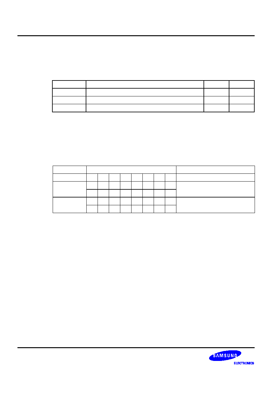
INSTRUCTION SET
KS57C0502/C0504/P0504 MICROCONTROLLER
580
SBC
Subtract with Carry
SBC
dst,src
Operation:
Operand
Operation Summary
Bytes
Cycles
A,@HL
Subtract indirect data memory from A with carry
1
1
EA,RR
Subtract register pair (RR) from EA with carry
2
2
RRb,EA
Subtract EA from register pair (RRb) with carry
2
2
Description:
SBC subtracts the source and carry flag value from the destination operand, leaving the result in
the destination. SBC sets the carry flag if a borrow is needed for the most significant bit;
otherwise it clears the carry flag. The contents of the source are unaffected.
If the carry flag was set before the SBC instruction was executed, a borrow was needed for the
previous step in multiple precision subtraction. In this case, the carry bit is subtracted from the
destination along with the source operand.
Operand
Binary Code
Operation Notation
A,@HL
0
0
1
1
1
1
0
0
C,A
A (HL) C
EA,RR
1
1
0
1
1
1
0
0
C, EA
EA RR C
1
1
0
0
1
r2
r1
0
RRb,EA
1
1
0
1
1
1
0
0
C,RRb
RRb EA C
1
1
0
0
0
r2
r1
0
Examples:
1.
The extended accumulator contains the value 0C3H, register pair HL the value 0AAH, and
the carry flag is set to "1":
SCF
; C
"1"
SBC
EA,HL
; EA
0C3H 0AAH 1H, C
"0"
JPS
XXX
; Jump to XXX; no skip after SBC
2.
If the extended accumulator contains the value 0C3H, register pair HL the value 0AAH, and
the carry flag is cleared to "0":
RCF
; C
"0"
SBC
EA,HL
; EA
0C3H 0AAH 0H = 19H, C
"0"
JPS
XXX
; Jump to XXX; no skip after SBC

KS57C0502/C0504/P0504 MICROCONTROLLER
INSTRUCTION SET
581
SBC
Subtract with Carry
SBC
(Continued)
Examples:
3.
If SBC A,@HL is followed by an ADS A,#im, the SBC skips on 'no borrow' to the instruction
immediately after the ADS. An 'ADS A,#im' instruction immediately after the 'SBC A,@HL'
instruction does not skip even if an overflow occurs. This function is useful for decimal
adjustment operations.
a.
8 6 decimal addition (the contents of the address specified by the HL register is 6H):
RCF
; C
"0"
LD
A,#8H
; A
8H
SBC
A,@HL
; A
8H 6H C(0) = 2H, C
"0"
ADS
A,#0AH
; Skip this instruction because no borrow after SBC result
JPS
XXX
b.
3 4 decimal addition (the contents of the address specified by the HL register is 4H):
RCF
; C
"0"
LD
A,#3H
; A
3H
SBC
A,@HL
; A
3H 4H C(0) = 0FH, C
"1"
ADS
A,#0AH
; No skip. A
0FH + 0AH = 9H
; (The skip function of 'ADS A,#im' is inhibited after a
; 'SBC A,@HL' instruction even if an overflow occurs.)
JPS
XXX
INSTRUCTION SET
KS57C0502/C0504/P0504 MICROCONTROLLER
582
SBS
Subtract
SBS
dst,src
Operation:
Operand
Operation Summary
Bytes
Cycles
A,@HL
Subtract indirect data memory from A; skip on borrow
1
1 + S
EA,RR
Subtract register pair (RR) from EA; skip on borrow
2
2 + S
RRb,EA
Subtract EA from register pair (RRb); skip on borrow
2
2 + S
Description:
The source operand is subtracted from the destination operand and the result is stored in the
destination. The contents of the source are unaffected. A skip is executed if a borrow occurs.
The value of the carry flag is not affected.
Operand
Binary Code
Operation Notation
A,@HL
0
0
1
1
1
1
0
1
A
A (HL); skip on borrow
EA,RR
1
1
0
1
1
1
0
0
EA
EA RR; skip on borrow
1
0
1
1
1
r2
r1
0
RRb,EA
1
1
0
1
1
1
0
0
RRb
RRb EA; skip on borrow
1
0
1
1
0
r2
r1
0
Examples:
1.
The accumulator contains the value 0C3H, register pair HL contains the value 0C7H, and the
carry flag is cleared to logic zero:
RCF
; C
"0"
SBS
EA,HL
; EA
0C3H 0C7H, C
"0"
; SBS instruction skips on borrow,
; but carry flag value is not affected
JPS
XXX
; Skip because a borrow occurred
JPS
YYY
; Jump to YYY is executed
2.
The accumulator contains the value 0AFH, register pair HL contains the value 0AAH, and
the carry flag is set to logic one:
SCF
; C
"1"
SBS
EA,HL
; EA
0AFH 0AAH, C
"1"
JPS
XXX
; Jump to XXX
; JPS was not skipped because no "borrow" occurred after SBS

KS57C0502/C0504/P0504 MICROCONTROLLER
INSTRUCTION SET
583
SCF
Set Carry Flag
SCF
Operation:
Operand
Operation Summary
Bytes
Cycles
--
Set carry flag to logic one
1
1
Description:
The SCF instruction sets the carry flag to logic one, regardless of its previous value.
Operand
Binary Code
Operation Notation
--
1
1
1
0
0
1
1
1
C
1
Example:
If the carry flag is cleared to logic zero, the instruction
SCF
sets the carry flag to logic one.
INSTRUCTION SET
KS57C0502/C0504/P0504 MICROCONTROLLER
584
SMB
Select Memory Bank
SMB
n
Operation:
Operand
Operation Summary
Bytes
Cycles
n
Select memory bank
2
2
Description:
The SMB instruction sets the upper four bits of a 12-bit data memory address to select a specific
memory bank. The constants 0, 1, and 15 are usually used as the SMB operand to select the
corresponding memory bank. All references to data memory addresses fall within the following
address ranges:
Please note that because data memory spaces differ for various devices in the SAM47 product
family, the 'n' value of the SMB instruction will also vary.
Addresses
Register Areas
Bank
SMB
000H01FH
Working registers
0
0
020H0FFH
Stack and general-purpose registers
100H1DFH
General-purpose registers
1
1
1E0H1FFH
Display registers
F80HFFFH
I/O-mapped hardware registers
15
15
The enable memory bank (EMB) flag must always be set to "1" in order for the SMB instruction
to execute successfully for memory banks 0, 1, and 15.
Format
Binary Code
Operation Notation
n
1
1
0
1
1
1
0
1
SMB
n (n = 0, 1, 15)
0
1
0
0
d3
d2
d1
d0
Example:
If the EMB flag is set, the instruction
SMB
0
selects the data memory address range for bank 0 (000H0FFH) as the working memory bank.
KS57C0502/C0504/P0504 MICROCONTROLLER
INSTRUCTION SET
585
SRB
Select Register Bank
SRB
n
Operation:
Operand
Operation Summary
Bytes
Cycles
n
Select register bank
2
2
Description:
The SRB instruction selects one of four register banks in the working register memory area. The
constant value used with SRB is 0, 1, 2, or 3. The following table shows the effect of SRB
settings:
ERB Setting
SRB Settings
Selected Register Bank
3
2
1
0
0
0
0
x
x
Always set to bank 0
0
0
Bank 0
1
0
0
0
1
Bank 1
1
0
Bank 2
1
1
Bank 3
NOTE: 'x' means don't care.
The enable register bank flag (ERB) must always be set for the SRB instruction to execute
successfully for register banks 0, 1, 2, and 3. In addition, if the ERB value is logic zero, register
bank 0 is always selected, regardless of the SRB value.
Operand
Binary Code
Operation Notation
n
1
1
0
1
1
1
0
1
SRB
n (n = 0, 1, 2, 3)
0
1
0
1
0
0
d1
d0
Example:
If the ERB flag is set, the instruction
SRB
3
selects register bank 3 (018H01FH) as the working memory register bank.
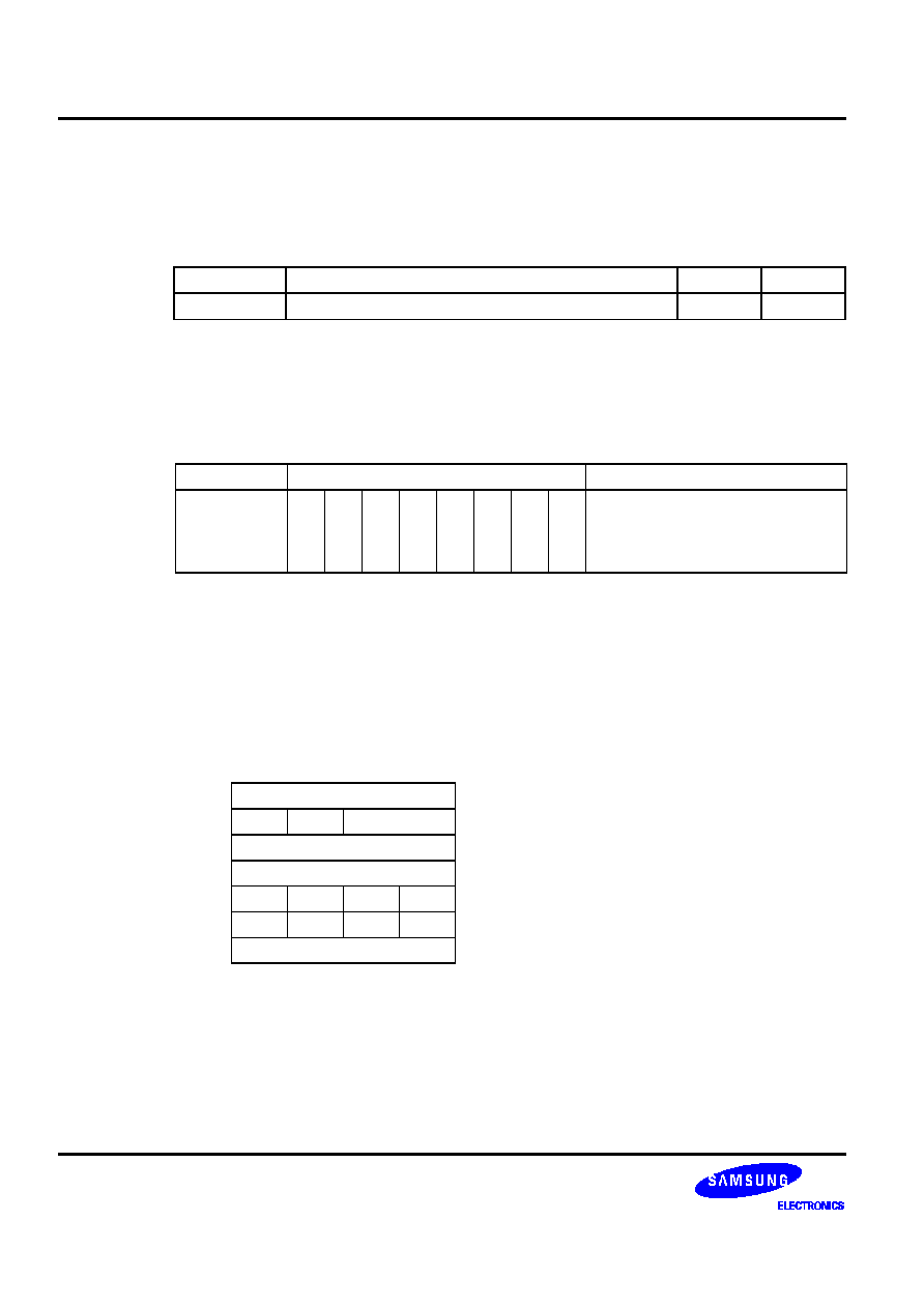
INSTRUCTION SET
KS57C0502/C0504/P0504 MICROCONTROLLER
586
SRET
Return from Subroutine and Skip
SRET
Operation:
Operand
Operation Summary
Bytes
Cycles
--
Return from subroutine and skip
1
3 + S
Description:
SRET is normally used to return to the previously executing procedure at the end of a subroutine
that was initiated by a CALL or CALLS instruction. SRET skips the resulting address, which is
generally the instruction immediately after the point at which the subroutine was called. Then,
program execution continues from the resulting address and the contents of the location
addressed by the stack pointer are popped into the program counter.
Operand
Binary Code
Operation Notation
--
1
1
1
0
0
1
0
1
PC138
(SP + 1) (SP)
PC70
(SP + 3) (SP + 2)
EMB,ERB
(SP + 5) (SP + 4)
SP
SP + 6
Example:
If the stack pointer contains the value 0FAH and RAM locations 0FAH, 0FBH, 0FCH, and 0FDH
contain the values 1H, 0H, 5H, and 2H, respectively, the instruction
SRET
leaves the stack pointer with the value 00H and the program returns to continue execution at
location 0125H.
During a return from subroutine, data is popped from the stack to the PC as follows:
SP
PC11 PC8
SP + 1
0
0
PC13 PC12
SP + 2
PC3 PC0
SP + 3
PC7 PC4
SP + 4
0
0
EMB
ERB
SP + 5
0
0
0
0
SP + 6
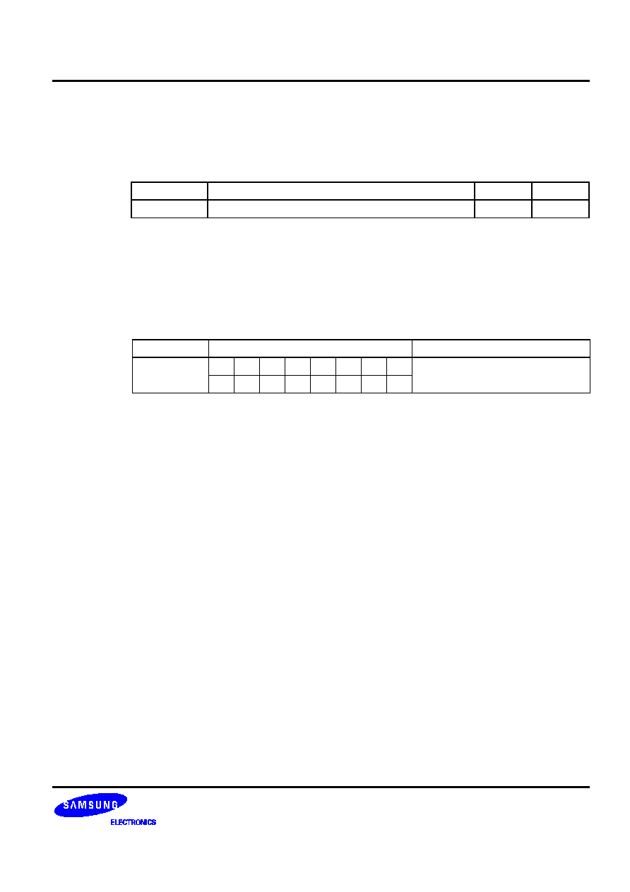
KS57C0502/C0504/P0504 MICROCONTROLLER
INSTRUCTION SET
587
STOP
Stop Operation
STOP
Operation:
Operand
Operation Summary
Bytes
Cycles
--
Engage CPU stop mode
2
2
Description:
The STOP instruction stops the system clock by setting bit 3 of the power control register
(PCON) to logic one. When STOP executes, all system operations are halted with the exception
of some peripheral hardware with special power-down mode operating conditions.
In application programs, a STOP instruction should be immediately followed by at least three
NOP instructions. This ensures an adequate time interval for the clock to stabilize before the
next instruction is executed.
Operand
Binary Code
Operation Notation
--
1
1
1
1
1
1
1
1
PCON.3
1
1
0
1
1
0
0
1
1
Example:
Given that bit 3 of the PCON register is cleared to logic zero, and all systems are operational,
the instruction sequence
STOP
NOP
NOP
NOP
sets bit 3 of the PCON register to logic one, stopping all controller operations (with the exception
of some peripheral hardware). The three NOP instructions provide the necessary timing delay for
clock stabilization before the next instruction in the program sequence is executed.
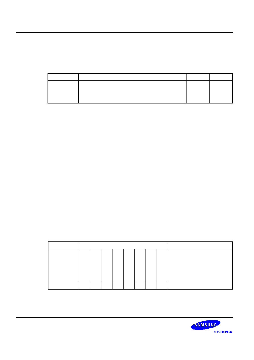
INSTRUCTION SET
KS57C0502/C0504/P0504 MICROCONTROLLER
588
VENT
Load EMB, ERB, and Vector Address
VENTn
dst
Operation:
Operand
Operation Summary
Bytes
Cycles
EMB (0,1)
ERB (0,1)
ADR
Load enable memory bank flag (EMB) and the enable
register bank flag (ERB) and program counter to
vector address, then branch to the corresponding
location.
2
2
Description:
The VENT instruction loads the contents of the enable memory bank flag (EMB) and enable
register bank flag (ERB) into the respective vector addresses. It then points the interrupt service
routine to the corresponding branching locations. The program counter is loaded automatically
with the respective vector addresses which indicate the starting address of the respective vector
interrupt service routines.
The EMB and ERB flags should be modified using VENT before the vector interrupts are
acknowledged. Then, when an interrupt is generated, the EMB and ERB values of the previous
routine are automatically pushed onto the stack and then popped back when the routine is
completed.
After the return from interrupt (IRET) you do not need to set the EMB and ERB values again.
Instead, use BITR and BITS to clear these values in your program routine.
The starting addresses for vector interrupts and reset operations are pointed to by the VENTn
instruction. These addresses must be stored in ROM locations 0000H3FFFH. Generally, the
VENTn instructions are coded starting at location 0000H.
The format for VENT instructions is as follows:
VENTn d1,d2,ADDR
EMB
d1 ("0" or "1")
ERB
d2 ("0" or "1")
PC
ADDR (address to branch
n = device-specific module address code (n = 0n)
Operand
Binary Code
Operation Notation
EMB (0,1)
ERB (0,1)
ADR
E
M
B
E
R
B
a13 a12 a11
a10
a9
a8
ROM (2 x n) 76
EMB, ERB
ROM (2 x n) 54
0, PC13,
PC12
ROM (2 x n) 30
PC128
ROM (2 x n + 1) 70
PC70
(n = 0, 1, 2, 3, 4, 5, 6, 7)
a7
a6
a5
a4
a3
a2
a1
a0

KS57C0502/C0504/P0504 MICROCONTROLLER
INSTRUCTION SET
589
VENT
Load EMB, ERB, and Vector Address
VENTn
(Continued)
Example:
The instruction sequence
ORG
0000H
VENT0
1,0,RESET
VENT1
0,1,INTB
VENT2
0,1,INT0
VENT3
0,1,INTS
VENT4
0,1,INTT0
VENT5
0,1,INTT1
causes the program sequence to branch to the RESET routine labeled 'RESET,' setting EMB to
"1" and ERB to "0" when
RESET
is activated. When a basic timer interrupt is generated, VENT1
causes the program to branch to the basic timer's interrupt service routine, INTB, and to set the
EMB value to "0" and the ERB value to "1". VENT2 then branches to INT0, VENT3 to INTS, and
so on, setting the appropriate EMB and ERB values.
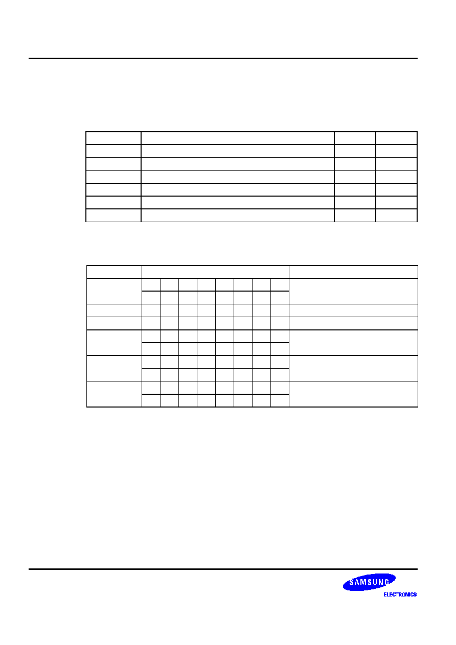
INSTRUCTION SET
KS57C0502/C0504/P0504 MICROCONTROLLER
590
XCH
Exchange A or EA with Nibble or Byte
XCH
dst,src
Operation:
Operand
Operation Summary
Bytes
Cycles
A,DA
Exchange A and data memory contents
2
2
A,Ra
Exchange A and register (Ra) contents
1
1
A,@RRa
Exchange A and indirect data memory
1
1
EA,DA
Exchange EA and direct data memory contents
2
2
EA,RRb
Exchange EA and register pair (RRb) contents
2
2
EA,@HL
Exchange EA and indirect data memory contents
2
2
Description:
The instruction XCH loads the accumulator with the contents of the indicated destination variable
and writes the original contents of the accumulator to the source.
Operand
Binary Code
Operation Notation
A,DA
0
1
1
1
1
0
0
1
A
DA
a7
a6
a5
a4
a3
a2
a1
a0
A,Ra
0
1
1
0
1
r2
r1
r0
A
Ra
A,@RRa
0
1
1
1
1
i2
i1
i0
A
(RRa)
EA,DA
1
1
0
0
1
1
1
1
A
DA,E
DA + 1
a7
a6
a5
a4
a3
a2
a1
a0
EA,RRb
1
1
0
1
1
1
0
0
EA
RRb
1
1
1
0
0
r2
r1
0
EA,@HL
1
1
0
1
1
1
0
0
A
(HL), E
(HL + 1)
0
0
0
0
0
0
0
1
Example:
Double register HL contains the address 20H. The accumulator contains the value 3FH
(00111111B) and internal RAM location 20H the value 75H (01110101B). The instruction
XCH
EA,@HL
leaves RAM location 20H with the value 3FH (00111111B) and the extended accumulator with
the value 75H (01110101B).

KS57C0502/C0504/P0504 MICROCONTROLLER
INSTRUCTION SET
591
XCHD
Exchange and Decrement
XCHD
dst,src
Operation:
Operand
Operation Summary
Bytes
Cycles
A,@HL
Exchange A and data memory contents; decrement
contents of register L and skip on borrow
1
2 + S
Description:
The instruction XCHD exchanges the contents of the accumulator with the RAM location
addressed by register pair HL and then decrements the contents of register L. If the content of
register L is 0FH, the next instruction is skipped. The value of the carry flag is not affected.
Operand
Binary Code
Operation Notation
A,@HL
0
1
1
1
1
0
1
1
A
(HL), then L
L1;
skip if L = 0FH
Example:
Register pair HL contains the address 20H and internal RAM location 20H contains the value
0FH:
LD
HL,#20H
LD
A,#0H
XCHD A,@HL
; A
0FH and L
L 1, (HL)
"0"
JPS
XXX
; Skipped because a borrow occurred
JPS
YYY
; H
2H, L
0FH
YYY
XCHD A,@HL
; (2FH)
0FH, A
(2FH), L
L 1 = 0EH
·
·
·
The 'JPS YYY' instruction is executed because a skip occurs after the XCHD instruction.
INSTRUCTION SET
KS57C0502/C0504/P0504 MICROCONTROLLER
592
XCHI
Exchange and Increment
XCHI
dst,src
Operation:
Operand
Operation Summary
Bytes
Cycles
A,@HL
Exchange A and data memory contents; increment
contents of register L and skip on overflow
1
2 + S
Description:
The instruction XCHI exchanges the contents of the accumulator with the RAM location
addressed by register pair HL and then increments the contents of register L. If the content of
register L is 0H, a skip is executed. The value of the carry flag is not affected.
Operand
Binary Code
Operation Notation
A,@HL
0
1
1
1
1
0
1
0
A
(HL), then L
L+1;
skip if L = 0H
Example:
Register pair HL contains the address 2FH and internal RAM location 2FH contains 0FH:
LD
HL,#2FH
LD
A,#0H
XCHI
A,@HL
; A
0FH and L
L + 1 = 0, (HL)
"0"
JPS
XXX
; Skipped because an overflow occurred
JPS
YYY
; H
2H, L
0H
YYY
XCHI
A,@HL
; (20H)
0FH, A
(20H), L
L + 1 = 1H
·
·
·
The 'JPS YYY' instruction is executed because a skip occurs after the XCHI instruction.

KS57C0502/C0504/P0504 MICROCONTROLLER
INSTRUCTION SET
593
XOR
Logical Exclusive OR
XOR
dst,src
Operation:
Operand
Operation Summary
Bytes
Cycles
A,#im
Exclusive-OR immediate data to A
2
2
A,@HL
Exclusive-OR indirect data memory to A
1
1
EA,RR
Exclusive-OR register pair (RR) to EA
2
2
RRb,EA
Exclusive-OR register pair (RRb) to EA
2
2
Description:
XOR performs a bitwise logical XOR operation between the source and destination variables and
stores the result in the destination. The source contents are unaffected.
Operand
Binary Code
Operation Notation
A,#im
1
1
0
1
1
1
0
1
A
A XOR im
0
0
1
1
d3
d2
d1
d0
A,@HL
0
0
1
1
1
0
1
1
A
A XOR (HL)
EA,RR
1
1
0
1
1
1
0
0
EA
EA XOR (RR)
0
0
1
1
1
r2
r1
0
RRb,EA
1
1
0
1
1
1
0
0
RRb
RRb XOR EA
0
0
1
1
0
r2
r1
0
Example:
If the extended accumulator contains 0C3H (11000011B) and register pair HL contains 55H
(01010101B), the instruction
XOR
EA,HL
leaves the value 96H (10010110B) in the extended accumulator.

INSTRUCTION SET
KS57C0502/C0504/P0504 MICROCONTROLLER
594
NOTES

Oscillator Circuits
Interrupts
Power-Down
RESET
I/O Ports
Timers and Timer/Counter
Comparator
Serial I/O Interface
Electrical Data
Mechanical Data
KS57P0504 OTP
Development Tools


KS57C0502/C0504/P0504 MICROCONTROLLER
OSCILLATOR CIRCUIT
61
6
OSCILLATOR CIRCUITS
OVERVIEW
The KS57C0502/C0504 has a system clock circuit. The CPU and peripheral hardware operate on the system
clock frequency supplied through these on-chip circuits. Specifically, a clock is required by the following
peripheral modules:
-- Basic timer
-- Timer/counter 0
-- Watch timer
-- Serial I/O interface
-- Clock output circuit
The system clock frequency can be divided by 4, 8, or 64. By manipulating PCON bits 1 and 0, you can select
one of the following frequencies as the cpu clock.
fx
4
,
fx
8
,
fx
64
When the PCON register is cleared to zero after
RESET
, the normal CPU operating mode is enabled, a system
clock of fx/64 is selected.
Bits 3 and 2 of the PCON register can be manipulated by a STOP or IDLE instruction to engage stop or idle
power-down mode.
OSCILLATOR CIRCUIT
KS57C0502/C0504/P0504 MICROCONTROLLER
62
OSCILLATOR
STOP
CPU
CLOCK
WAIT RELEASE SIGNAL
INTERNAL
RESET
SIGNAL
POWER-DOWN RELEASE SIGNAL
PCON.3,2 CLEAR
X
in
X
out
fx
CPU STOP SIGNAL
( IDLE MODE)
IDLE
STOP
WATCH TIMER
BASIC TIMER
TIMER/COUNTER 0
CLOCK OUTPUT CIRCIT
COMPARATOR
1/4
OSCILLATOR
CONTROL
CIRCUIT
SYSTEM
OSCILLATOR
CIRCUIT
FREQUENCY
DIVIDING
CIRCUIT
1/2
1/16
SELECTOR
PCON.0
PCON.1
PCON.2
PCON.3
Figure 61. Clock Circuit Diagram
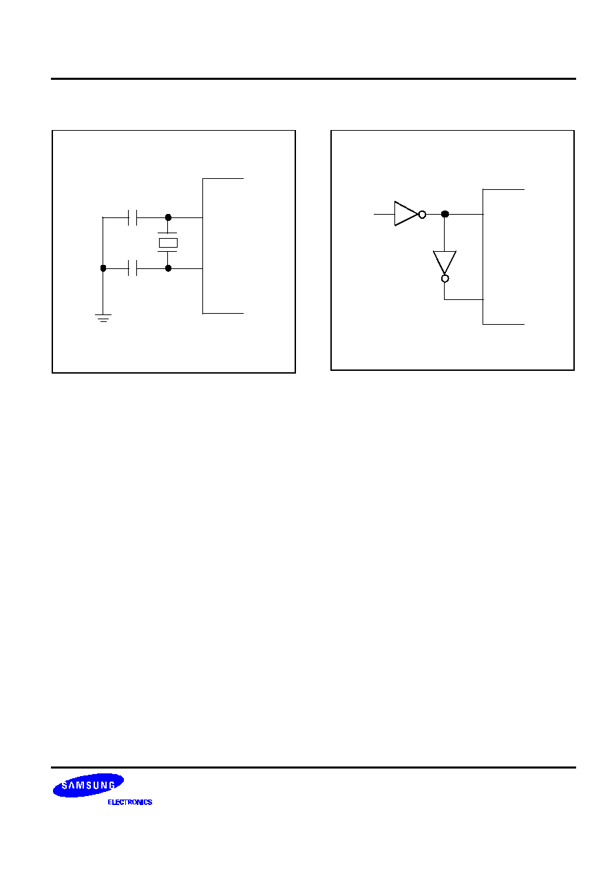
KS57C0502/C0504/P0504 MICROCONTROLLER
OSCILLATOR CIRCUIT
63
SYSTEM OSCILLATOR CIRCUITS
X
in
X
out
Figure 62. Crystal/Ceramic Oscillator
X
in
X
out
Figure 63. External Clock
OSCILLATOR CIRCUIT
KS57C0502/C0504/P0504 MICROCONTROLLER
64
POWER CONTROL REGISTER (PCON)
The power control register, PCON, is a 4-bit register that is used to select the CPU clock frequency and to
control CPU operating and power-down modes. PCON is mapped to RAM address FB3H and can be addressed
directly by 4-bit write instructions or by the instructions IDLE and STOP.
FB3H
PCON.3
PCON.2
PCON.1
PCON.0
PCON bits 3 and 2 are controlled by the STOP and IDLE instructions to engage the idle and stop power-down
modes. Idle and stop modes can be initiated by these instruction despite the current value of the enable memory
bank flag (EMB). PCON bits 1 and 0 are used to select a specific system clock frequency.
RESET
sets PCON register values to logic zero. PCON.1 and PCON.0 divide the frequency (fx) by 64, 8, and
4. PCON.3 and PCON.2 enable normal CPU operating mode.
Table 61. Power Control Register (PCON) Organization
+
+
PROGRAMMING TIP -- Setting the CPU Clock
To set the CPU clock to 0.95 µs at 4.19 MHz:
BITS
EMB
SMB
15
LD
A,#3H
LD
PCON,A
PCON Bit Settings
Resulting CPU Operating Mode
PCON.3
PCON.2
0
0
Normal CPU operating mode
0
1
Idle power-down mode
1
0
Stop power-down mode
PCON Bit Settings
Resulting CPU Clock Frequency
PCON.1
PCON.0
0
0
fx/64
1
0
fx/8
1
1
fx/4
KS57C0502/C0504/P0504 MICROCONTROLLER
OSCILLATOR CIRCUIT
65
INSTRUCTION CYCLE TIMES
The unit of time that equals one machine cycle varies depending on how the oscillator clock signal is divided
(by 4, 8, or 64). Table 62 shows corresponding cycle times in microseconds.
Table 62. Instruction Cycle Times for CPU Clock Rates
Selected
CPU Clock
Resulting Frequency
Oscillation
Source
Cycle Time (µsec)
fx/64
65.5 kHz
15.3
fx/8
524.0 kHz
fx = 4.19 MHz
1.91
fx/4
1.05 MHz
0.95
CLOCK OUTPUT MODE REGISTER (CLMOD)
The clock output mode register, CLMOD, is a 4-bit register that is used to enable or disable clock output to the
CLO pin and to select the CPU clock source and frequency. CLMOD is mapped to RAM address FD0H and is ad-
dressable by 4-bit write instructions only.
FD0H
CLMOD.3
"0"
CLMOD.1
CLMOD.0
RESET
clears CLMOD to logic zero, which automatically selects the CPU clock as the clock source (without
initiating clock oscillation), and disables clock output.
CLMOD.3 is the enable/disable clock output control bit; CLMOD.1 and CLMOD.0 are used to select one of
four possible clock sources and frequencies: normal CPU clock, fx/8, fx/16, or fx/64.
Table 63. Clock Output Mode Register (CLMOD) Organization
CLMOD Bit Settings
Resulting Clock Output
CLMOD.1
CLMOD.0
Clock Source
Frequency
0
0
CPU clock (fx/4, fx/8, fx/64)
1.05 MHz, 524 kHz, 65.5 kHz
0
1
fx/8
524 kHz
1
0
fx/16
262 kHz
1
1
fx/64
65.5 kHz
CLMOD.3
Result of CLMOD.3 Setting
0
Clock output is disabled
1
Clock output is enabled
NOTE: Frequencies assume that fx = 4.19 MHz.
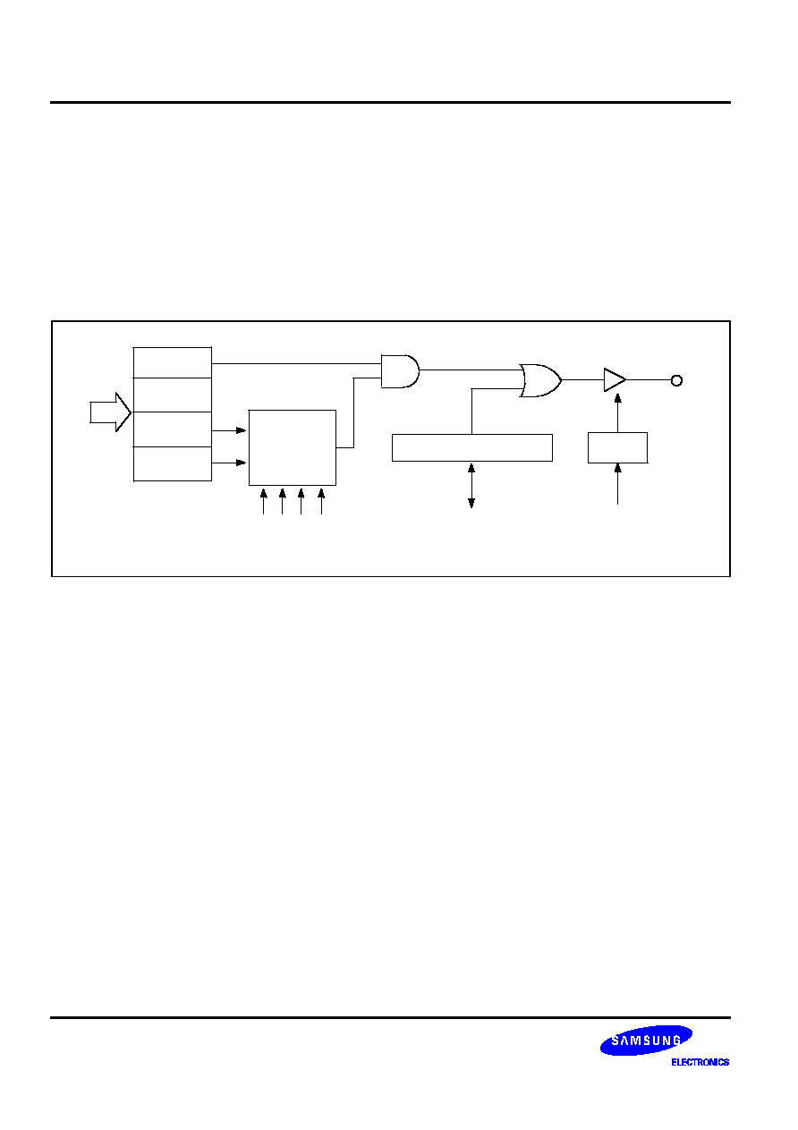
OSCILLATOR CIRCUIT
KS57C0502/C0504/P0504 MICROCONTROLLER
66
CLOCK OUTPUT CIRCUIT
The clock output circuit, used to output clock pulses to the CLO pin, has the following components:
-- 4-bit clock output mode register (CLMOD)
-- Clock selector
-- Output latch
-- Port mode flag
-- CLO output pin (P3.2)
CLO
CLOCKS
4
(fx/8, fx/16, fx/64, CPU clock)
CLMOD.3
CLMOD.2
CLMOD.1
CLMOD.0
PM3.2
P3.2 OUTPUT LATCH
CLOCK
SELECTOR
Figure 64. CLO Output Pin Circuit Diagram
CLOCK OUTPUT PROCEDURE
To output clock pulses to the CLO pin, follow this general procedure:
1.
Disable clock output by clearing CLMOD.3 to logic zero.
2.
Set the clock output frequency (CLMOD.1, CLMOD.0).
3.
Load a "0" to the output latch of the CLO pin (P3.2).
4.
Set the P3.2 mode flag (PM3.2) to output mode.
5.
Enable clock output by setting CLMOD.3 to logic one.
+
+
PROGRAMMING TIP -- CPU Clock Output to the CLO Pin
To output the CPU clock to the CLO pin:
BITS
EMB
;
Or BITR EMB
SMB
15
LD
EA,#40H
LD
PMG1,EA
;
P3.2
Output mode
BITR
P3.2
;
Clear P3.2 output latch
LD
A,#9H
LD
CLMOD,A
KS57C0502/C0504/P0504 MICROCONTROLLER
INTERRUPTS
71
7
INTERRUPTS
OVERVIEW
KS57C0502/C0504 microcontrollers process three types of interrupts:
--
Internal interrupts generated by on-chip processes
--
External interrupts generated by external peripheral devices
--
Quasi-interrupts used for edge detection and clock sources
Table 71. Interrupts and Corresponding I/O Pin(s)
Interrupt Type
Interrupt Name
I/O Port Pin(s)
External Interrupts
INT0, INT1
P1.0, P1.1
Internal Interrupts
INTB, INTT0, INTS
Not applicable
Quasi-interrupts
INTK
P6.0P6.2 (KS0KS2)
INTW
Not applicable
The interrupt control circuit has four functional components:
-- Interrupt enable flags (IEx)
-- Interrupt request flags (IRQx)
-- Interrupt priority registers (IME and IPR)
-- Power-down release signal circuit
Vectored Interrupts
Interrupt requests may be processed as vectored interrupts in hardware, or they can be generated by program
software. A vectored interrupt is generated when the following flags and register settings, corresponding to the
specific interrupt, are enabled (set to logic one):
-- Interrupt enable flag (IEx)
-- Interrupt master enable flag (IME)
-- Interrupt request flag (IRQx)
-- Interrupt status flags (IS0, IS1)
-- Interrupt priority register (IPR)
If all conditions are satisfied, the start address of the interrupt is loaded into the program counter and the pro-
gram starts executing the service routine from this address.

INTERRUPTS
KS57C0502/C0504/P0504 MICROCONTROLLER
72
Vectored Interrupts (Continued)
EMB and ERB flags for RAM memory and register banks are stored in the vector address area of the ROM
during interrupt service routines. The flags are stored at the beginning of the program with the VENT instruction.
Enable flag values are saved during the main routine, as well as during service routines. Any changes you make
to enable flag values during a service routine are not stored in the vector address.
When an interrupt occurs, the enable flag values before the interrupt is initiated are saved along with the pro-
gram status word (PSW), and the enable flag values for the interrupt is fetched from the respective vector
address.
Then, if required, you can modify the enable flags during the interrupt service routine. When the interrupt ser-
vice routine is returned to the main routine by the IRET instruction, however, the original values saved in the
stack are restored and the main program continues program execution with these values.
Software-Generated Interrupts
To generate an interrupt request from software, the program manipulates the appropriate IRQx flag. When the
interrupt request value in the IRQx flag is set, it is retained until all other conditions for the interrupt have been
met, and the service routine can be initiated.
Multiple Interrupts
By manipulating the two interrupt status flags (IS0 and IS1), you can control service routine initialization and
thereby process multiple interrupts simultaneously.
Power-Down Mode Release
An interrupt (with the exception of INT0) can be used to release power-down mode (stop or idle). Interrupts for
power-down mode release are initiated by setting the corresponding interrupt enable flag. Even if the IME flag is
cleared to zero, power-down mode will be released by an interrupt request signal when the interrupt enable flag
has been set. In such cases, the interrupt routine will not be executed since IME = "0".
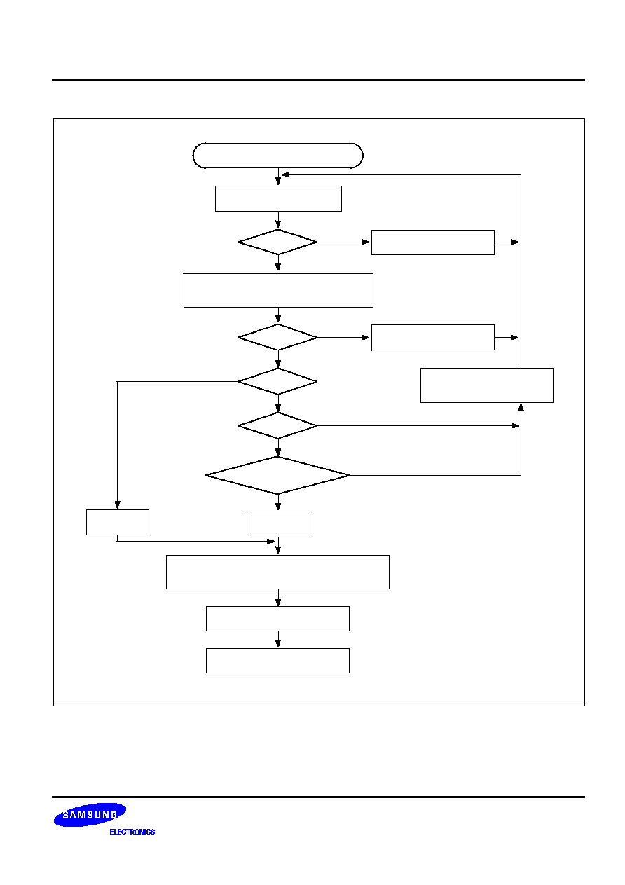
KS57C0502/C0504/P0504 MICROCONTROLLER
INTERRUPTS
73
Request flag (IRQx) <-- 1
Interrupt is generated (INT xx)
Generate corresponding vector interrupt
and release power-down mode
High-priority interrupt?
IS1,0 = 0,0?
IS1,0 = 0,1 ?
Store contents of PC and PSW in the stack area;
set PC contents to corresponding vector address
IS1,0 = 0,1
Reset corresponding IRQx flag
Jump to interrupt start address
Retain value until interrupt
service routine is completed
Retain value until IME = 1
IME = 1?
IS1,0 = 1,0
NO
NO
NO
NO
YES
YES
YES
YES
YES
NO
Retain value until IEx = 1
IEx = 1?
Figure 71. Interrupt Execution Flowchart
INTERRUPTS
KS57C0502/C0504/P0504 MICROCONTROLLER
74
IRQB
IRQ0
IRQ1
IRQS
IRQT0
IRQW
IRQK
IET0
IES
IE1
IE0
IEB
IMOD1
IMOD0
INTB
INT0
INT1
INTS
INTT0
INTW
#
@
@
POWER-DOWN
MODE
RELEASE SIGNAL
IME
IPR
IS1 IS0
INTERRUPT CONTROL UNIT
VECTOR INTERRUPT
GENERATOR
# = Noise filtering circuit
@ = Edge detection circuit
IMODK
INTK (KS0KS2)
IEW
IEK
Figure 72. Interrupt Control Circuit Diagram
KS57C0502/C0504/P0504 MICROCONTROLLER
INTERRUPTS
75
MULTIPLE INTERRUPTS
The interrupt controller can service multiple interrupts in two ways: as two-level interrupts, where either all
interrupt requests or only those of highest priority are serviced, or as multi-level interrupts, when the interrupt
service routine for a lower-priority request is accepted during the execution of a higher priority routine.
Two-Level Interrupt Handling
Two-level interrupt handling is the standard method for processing multiple interrupts. When the IS1 and IS0
bits of the PSW (FB0H.3 and FB0H.2, respectively) are both logic zero, program execution mode is normal and
all interrupt requests are serviced. See Figure 73.
Whenever an interrupt request is accepted, IS1 and IS0 are incremented by one ("0"
"1" or "1"
"0"), and
the values are stored in the stack along with the other PSW bits. After the interrupt routine has been serviced,
the modified IS1 and IS0 values are automatically restored from the stack by an IRET instruction.
IS0 and IS1 can be manipulated directly by 1-bit write instructions, regardless of the current value of the
enable memory bank flag (EMB). Before you can modify an interrupt service flag, however, you must first disable
interrupt processing with a DI instruction.
When you set IS1 to "0" and IS0 to "1", you inhibit all interrupt service routines except for the highest priority
interrupt currently defined by the interrupt priority register (IPR).
INT DISABLE
SET IPR
INT ENABLE
LOW OR
HIGH LEVEL
INTERRUPT
GENERATED
NORMAL PROGRAM
PROCESSING
(STATUS 0)
HIGH-LEVEL
INTERRUPT
GENERATED
HIGH OR LOW LEVEL
INTERRUPT PROCESSING
(STATUS 1)
HIGH LEVEL INTERRUPT
PROCESSING
(STATUS 2)
Figure 73. Two-Level Interrupt Handling
Multi-Level Interrupt Handling
With multi-level interrupt handling, a lower-priority interrupt request can be executed while a high-priority inter-
rupt is being serviced. This is done by manipulating the interrupt status flags, IS0 and IS1. See Figure 74.
When an interrupt is requested during normal program execution, the interrupt status flags IS0 and IS1 are set
to "0" and "1", respectively. This setting allows only highest-priority interrupts to be serviced. When a high-priority
request is accepted, both interrupt status flags are then cleared to "0" by software so that a request of any priority
level can be serviced. In this way, the high-priority and low-priority requests will be serviced in parallel.
INTERRUPTS
KS57C0502/C0504/P0504 MICROCONTROLLER
76
Table 72. IS1 and IS0 Function
Process Status
Before INT
Effect of ISx Bit Setting
After INT ACK
IS1
IS0
IS1
IS0
0
0
0
All interrupt requests are serviced.
0
1
1
0
1
Only high-priority interrupts as determined by the
current settings in the IPR register are serviced.
1
0
2
1
0
No additional interrupt requests will be serviced.
--
--
--
1
1
Value undefined
--
--
INT DISABLE
SET IPR
INT ENABLE
LOW OR
HIGH LEVEL
INTERRUPT
GENERATED
NORMAL PROGRAM
PROCESSING
(STATUS 0)
LOW OR
HIGH LEVEL
INTERRUPT
GENERATED
SINGLE
INTERRUPT
2-LEVEL
INTERRUPT
STATUS 1
STATUS 1
STATUS 0
STATUS 0
INT ENABLE
MODIFY STATUS
INT DISABLE
HIGH-LEVEL
INTERRUPT
GENERATED
STATUS 2
3-LEVEL
INTERRUPT
Figure 74. Multiple-Level Interrupt Handling
KS57C0502/C0504/P0504 MICROCONTROLLER
INTERRUPTS
77
INTERRUPT PRIORITY REGISTER (IPR)
The 4-bit interrupt priority register (IPR) is used to control multi-level interrupt handling. The IPR is mapped to
RAM address FB2H, and its reset value is logic zero. Before the IPR can be modified by 4-bit write instructions,
all interrupts must first be disabled by a DI instruction.
FB2H
IME
IPR.2
IPR.1
IPR.0
By manipulating the IPR settings, you can choose to process all interrupt requests with the same priority level,
or you can select one type of interrupt for high-priority processing. A low-priority interrupt can itself be interrupted
by a high-priority interrupt, but not by another low-priority interrupt. A high-priority interrupt cannot be interrupted
by any other interrupt source.
Interrupt
Default Priority
INTB
1
INT0
2
INT1
3
INTS
4
INTT0
5
The MSB of the IPR, the interrupt master enable flag (IME), enables and disables all interrupt processing.
Even if an interrupt request flag and its corresponding enable flag are set, a service routine cannot be executed
until the IME flag is set to logic one.
The IME flag is mapped to FB2H.3 and can be directly manipulated by EI and DI instructions, regardless of
the current enable memory bank (EMB) value.
Table 74. Interrupt Priority Register Settings
IPR.2
IPR.1
IPR.0
Result of IPR Bit Setting
0
0
0
Process all interrupt requests at low priority.
0
0
1
Process INTB interrupt only.
0
1
0
Process INT0 interrupts only.
0
1
1
Process INT1 interrupts only.
1
0
0
Process INTS interrupts only.
1
0
1
Process INTT0 interrupts only.
NOTE: When all interrupts are low priority (the lower three bits of the IPR register are logic zero), the interrupt generated
first will become high priority. Therefore, the first generated interrupt cannot be superceded by any other interrupt. If
two or more interrupt requests are received simultaneously, the priority level is determined according to the
standard interrupt priorities in Table 7.4 (e.g., the default priority assigned by hardware when the lower three IPR
bits = "0"). In this case, the higher-priority interrupt request is serviced and the other interrupt is inhibited. Then,
when the high-priority interrupt is returned from its service routine by an IRET instruction, the inhibited interrupt
service routine is started.
INTERRUPTS
KS57C0502/C0504/P0504 MICROCONTROLLER
78
+
+
PROGRAMMING TIP -- Setting the INT Interrupt Priority
Set the INT1 interrupt to high priority:
BITS
EMB
SMB
15
DI
;
IPR.3 (IME)
0
LD
A,#3H
LD
IPR,A
EI
;
IPR.3 (IME)
1
EXTERNAL INTERRUPT MODE REGISTERS (IMOD0, IMOD1)
The following components are used to process external interrupts at the INT0 and INT1 pin:
-- Noise filtering circuit for INT0
-- Edge detection circuit
-- Two mode registers, IMOD0 and IMOD1
The mode registers are used to control the triggering edge of the input signal. IMOD settings let you choose
either the rising or falling edge of the incoming signal at the INT0 and INT1 pins as the interrupt request trigger.
FB4H
IMOD0.3
"0"
IMOD0.1
IMOD0.0
FB5H
"0"
"0"
"0"
IMOD1.0
IMOD0 and IMOD1 bits are mapped to RAM addresses FB4H (IMOD0) and FB5H (IMOD1), and are
addressable by 4-bit write instructions.
RESET
clears all IMOD values to logic zero, selecting rising edges as the
trigger for incoming interrupt requests.
Table 75. IMOD0 and IMOD1 Register Organization
IMOD0
IMOD0.3
0
IMOD0.1
IMOD0.0
Effect of IMOD0 Settings
0
Select CPU clock for sampling
1
Select fx/64 sampling clock
0
0
Rising edge detection
0
1
Falling edge detection
1
0
Both rising and falling edge detection
1
1
IRQ0 flag cannot be set to "1"
IMOD1
0
0
0
IMOD1.0
Effect of IMOD1 Settings
0
Rising edge detection
1
Falling edge detection
KS57C0502/C0504/P0504 MICROCONTROLLER
INTERRUPTS
79
EXTERNAL INTERRUPT 0 and 1 MODE REGISTERS (Continued)
When a sampling clock rate of fx/64 is used for INT0, an interrupt request flag must be cleared before 16 ma-
chine cycles have elapsed. Since the INT0 pin has a clock-driven noise filtering circuit built into it, please take
the following precautions when you use it:
-- To trigger an interrupt, the input signal width at INT0 must be at least two times wider than the pulse width
of the clock selected by IMOD0. This is true even when the INT0 pin is used for general-purpose input.
-- Since the INT0 input sampling clock does not operate during stop or idle mode, you cannot use INT0 to re-
lease power-down mode.
INT0
CPU clock
fx/64
INT1
NOISE FILTER
EDGE DETECTION
IRQ0
IMOD0
IMOD1
CLOCK
SELECTOR
P1.1
P1.0
EDGE DETECTION
IRQ1
Figure 75. Circuit Diagram for INT0 and INT1 Pins
When modifying the IMOD0 and IMOD1 registers, it is possible to accidentally set an interrupt request flag. To
avoid unwanted interrupts, take these precautions when writing your programs:
1.
Disable all interrupts with a DI instruction.
2.
Modify the IMOD0 or IMOD1 register.
3.
Clear all relevant interrupt request flags.
4.
Enable the interrupt by setting the appropriate IEx flag.
5.
Enable all interrupts with an EI instructions.
INTERRUPTS
KS57C0502/C0504/P0504 MICROCONTROLLER
710
KEY INTERRUPT MODE REGISTER (IMODK)
The mode register for external interrupts at the KS0KS2 pins, IMODK, is a 4-bit register at RAM address
FB6H. IMODK is addressable only by 4-bit write instructions.
RESET
clears all IMODK bits to logic zero.
FB6H
"0"
IMODK.2 IMODK.1 IMODK.0
When bits in the IMODK register are set to logic one, INTK uses the falling edge of an incoming signal at
corresponding pins as the interrupt request trigger. When a falling edge is detected at any one of the pins KS0
KS2, the IRQK flag is set to logic one and a release signal for power-down mode is generated.
Table 76. IMODK Register Bit Settings
IMODK
0
IMODK.2
IMODK.1
IMODK.0
Effect of IMODK Settings
0
0
0
Disable key interrupt
0
0
1
Select falling edge at KS0
0
1
0
Select falling edge at KS1
0
1
1
Select falling edge at KS0KS1
1
0
0
Select falling edge at KS2
1
0
1
Select falling edge at KS0, KS2
1
1
0
Select falling edge at KS1KS2
1
1
1
Select falling edge at KS0KS2
KS2
KS1
KS0
FALLING
EDGE
DETECTION
CIRCUIT
1. To generate a key interrupt on a falling edge at KS0KS2, all KS0KS2 pins must be configured
to input mode.
2. If anyone of the KS0-KS2 pins used for interrupt stays low, a key interrupt is not generated.
Since all KS0-KS2 pins are ANDed, the falling edge detection circuit cannot detects a falling edge.
NOTES:
IRQK
IMODK
Figure 76. Circuit Diagram for KS0KS2 Pins

KS57C0502/C0504/P0504 MICROCONTROLLER
INTERRUPTS
711
+
+
PROGRAMMING TIP -- Using INTK as a Key Input Interrupt
When the INTK interrupt used as a key interrupt, the key interrupt pin must be set to input.
1.
When KS0KS2 are selected:
BITS
EMB
SMB
15
LD
A,#3H
LD
IMODK,A
;
(IMODK)
#3H, KS0KS2 falling edge select
LD
EA,#00H
LD
PMG3,EA
;
P6
Input mode
LD
EA,#40H
LD
PUMOD,EA
;
Enable P6 pull-up resistors

INTERRUPTS
KS57C0502/C0504/P0504 MICROCONTROLLER
712
INTERRUPT FLAGS
There are three types of interrupt flags: interrupt request and interrupt enable flags that correspond to each in-
terrupt, the interrupt master enable flag, which enables or disables all interrupt processing.
Interrupt Master Enable Flag (IME)
The interrupt master enable flag, IME, enables or disables all interrupt processing. Therefore, even when an
IRQx flag is set and its corresponding IEx flag is enabled, the interrupt service routine is not executed until the
IME flag is set to logic one.
The IME flag is located in the IPR register (IPR.3), and is mapped to bit address FB2H.3. It can be directly be
manipulated by EI and DI instructions, regardless of the current value of the enable memory bank flag (EMB).
Interrupt Enable Flags (IEx)
IEx flags, when set to logic one, enable specific interrupt requests to be serviced. When the interrupt request
flag is set to logic one, an interrupt will not be serviced until its corresponding IEx flag is also enabled.
Interrupt enable flags are mapped to the RAM address area FB8HFBFH, and can be read, written, or tested
directly by 1-bit instructions (BITS and BITR). IEx flags can be addressed directly at their specific RAM
addresses, despite the current value of the enable memory bank (EMB) flag.
Interrupt Request Flags (IRQx)
Interrupt request flags, located in the RAM area FB8H-FBFH, are read/write addressable by 1-bit or 4-bit in-
structions. IRQx flags can be addressed directly at their specific RAM addresses, regardless of the current value
of the enable memory bank (EMB) flag.
When a specific IRQx lag is set to logic one, the corresponding interrupt request is generated. The flag is then
automatically cleared to logic zero by hardware when the interrupt has been serviced. Exceptions are the watch
timer interrupt request flag, IRQW, and key interrupt request flag IRQK, which must be cleared by software after
the interrupt service routine has executed. IRQx flags are also used to execute interrupt requests from software.
In summary, follow these guidelines for using IRQx flags:
1.
IRQx is set to request an interrupt when an interrupt meets the set condition for interrupt generation.
2.
IRQx is set to "1" by hardware and then cleared by hardware when the interrupt has been serviced (with
the exception of IRQW and IRQ2).
3.
When IRQx is set to "1" by software, an interrupt is generated.
KS57C0502/C0504/P0504 MICROCONTROLLER
INTERRUPTS
713
INTERRUPT MASTER ENABLE FLAG (IME)
The interrupt master enable flag, IME, inhibits or enables all interrupt processing. Therefore, even when an
IRQx flag and its corresponding IEx flag is enabled, an interrupt request will not be serviced until the IME flag is
set to logic one. The IME flag is the most significant bit of the 4-bit IPR register at RAM location FB2H.
IME
IPR.2
IPR.1
IPR.0
Effect of Bit Settings
0
Inhibit all interrupts
1
Enable all interrupts
You can manipulate the IME flag using EI and DI instructions, despite the current value of the enable memory
bank (EMB) flag.
INTERRUPT ENABLE FLAGS (IEx)
Interrupt enable flags are used to control the execution of service routines for specific interrupt requests. The
enable flag has priority over a request flag -- even if the IRQx flag is enabled, the interrupt request will not be
serviced until the corresponding IEx flag is set to logic one.
Using 1-bit or 4-bit instructions and direct addressing, you can read, write, or test IEx (and IRQx) flags despite
the current enable memory bank (EMB) value. The IEx and IRQx flags are mapped to RAM area FB8HFBFH.
Table 77. Interrupt Enable and Interrupt Request Flag Addresses
Address
Bit 3
Bit 2
Bit 1
Bit 0
FB8H
0
0
IEB
IRQB
FBAH
0
0
IEW
IRQW
FBBH
0
0
0
0
FBCH
0
0
IET0
IRQT0
FBDH
0
0
IES
IRQS
FBEH
IE1
IRQ1
IE0
IRQ0
FBFH
0
0
IEK
IRQK
NOTES:
1.
IEx refers generically to all interrupt enable flags.
2.
IRQx refers generically to all interrupt request flags.
3.
IEx = 0 is interrupt disable mode.
4.
IEx = 1 is interrupt enable mode.
INTERRUPTS
KS57C0502/C0504/P0504 MICROCONTROLLER
714
INTERRUPT REQUEST FLAGS (IRQx)
When an interrupt request flag (IRQx) is set, a software-generated interrupt is enabled for the corresponding
interrupt. IRQx flags can be written by 1- or 4-bit RAM control instructions. IRQx flags are then cleared
automatically when the interrupt has been serviced. Exceptions to the general rule are the watch timer interrupt
request flag, IRQW and key interrupt request flag, IRQK; they must be cleared by software after the interrupt
service routine has executed.
Table 78. Interrupt Request Flag Conditions and Priorities
Interrupt
Source
Internal /
External
Pre-condition for IRQx Flag Setting
Interrupt
Priority
IRQx Flag
Name
INTB
I
Reference time interval signal from basic timer
1
IRQB
INT0
E
Rising or falling edge detected at INT0 pin
2
IRQ0
INT1
E
Rising or falling edge detected at INT1 pin
3
IRQ1
INTS
I
Completion signal for serial transmit-and-re-
ceive or receive-only operation
4
IRQS
INTT0
I
Signals for TCNT0 and TREF0 registers coin-
cide
5
IRQT0
INTK
*
E
Falling edge is detected at any one of the KS0
KS2 pins
--
IRQK
INTW
*
I
Time interval of 0.5 secs or 3.19 msecs
--
IRQW
*
INTK and INTW are quasi-interrupts and INTK is used only for testing incoming signals.

KS57C0502/C0504/P0504 MICROCONTROLLER
POWER-DOWN
81
8
POWER-DOWN
OVERVIEW
The KS57C0502/C0504 microcontroller has two power-down modes to reduce power consumption: idle and
stop. Idle mode is initiated by the IDLE instruction and stop mode by the instruction STOP. (Several NOP
instructions must always follow an IDLE or STOP instruction in a program.) In idle mode, the CPU clock stops
while peripherals and the oscillation source continue to operate normally.
When
RESET
occurs during normal operation or during a power-down mode, a reset operation is initiated and
the CPU enters idle mode. When the standard oscillation stabilization time interval (31.3 ms at 4.19 MHz) has
elapsed, normal CPU operation resumes.
In stop mode, system clock oscillation is halted (assuming it is currently operating), and peripheral hardware
components are powered-down. The effect of stop mode on specific peripheral hardware components -- CPU,
basic timer, serial I/O, timer/ counters 0, and watch timer -- and on external interrupt requests, is detailed in
Table 81.
NOTE
Do not use stop mode if you are using an external clock source because X
in
input must be
restricted internally to V
SS
to reduce current leakage.
Idle or stop modes are terminated either by a
RESET
, or by an interrupt with the exception of INT0, which are
enabled by the corresponding interrupt enable flag, IEx. When power-down mode is terminated by
RESET
input,
a normal reset operation is executed. Assuming that both the interrupt enable flag and the interrupt request flag
are set to "1", power-down mode is released immediately upon entering power-down mode.
When an interrupt is used to release power-down mode, the operation differs depending on the value of the
interrupt master enable flag (IME):
-- If the IME flag = "0", program execution is started immediately after the instruction which issues the
request to enter power-down mode. The interrupt request flag remains set to logic one.
-- If the IME flag = "1", two instructions are executed after the power-down mode release. Then, the vectored
interrupt is initiated. However, when the release signal is caused by INTK or INTW, the operation is
identical to the IME = 0 condition. That is, a vector interrupt is not generated.
POWER-DOWN
KS57C0502/C0504/P0504 MICROCONTROLLER
82
Table 81. Hardware Operation During Power-Down Modes
Operation
Stop Mode (STOP)
Idle Mode (IDLE)
Clock oscillator
System clock oscillation stops
CPU clock oscillation stops (system
clock oscillation continues)
Basic timer
Basic timer stops
Basic timer operates (with IRQB set at
each reference interval)
Serial interface
Operates only if external
SCK
input is
selected as the serial I/O clock
Operates if a clock other than the CPU
clock is selected as the serial I/O clock
Timer/counter 0
Operates only if TCL0 is selected as the
counter clock
Timer/counter 0 operates
Comparator
Comparator operation is stopped
Comparator operates
Watch timer
Watch timer operation is stopped
Watch timer operates
External interrupts
INT1 and INTK are acknowledged; INT0
is not serviced
INT1 and INTK are acknowledged;
INT0 is not serviced
CPU
All CPU operations are disabled
All CPU operations are disabled
Power-down mode
release signal
Interrupt request signals (except INT0)
are enabled by an interrupt enable flag or
by
RESET
input
Interrupt request signals (except INT0)
are enabled by an interrupt enable flag or
by
RESET
input
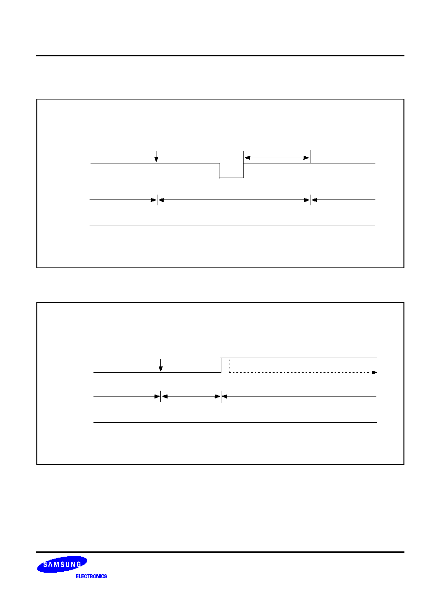
KS57C0502/C0504/P0504 MICROCONTROLLER
POWER-DOWN
83
IDLE MODE TIMING DIAGRAMS
CLOCK
SIGNAL
IDLE
INSTRUCTION
OSCILLATION
STABILIZATION
(31.3 ms / 4.19 MHz)
NORMAL MODE
IDLE MODE
NORMAL MODE
NORMAL OSCILLATION
RESET
Figure 81. Timing When Idle Mode is Released by
RESET
NORMAL MODE
IDLE MODE
NORMAL MODE
NORMAL OSCILLATION
MODE
RELEASE
SIGNAL
IDLE
INSTRUCTION
CLOCK
SIGNAL
INTERRUPT ACKNOWLEDGE (IME = 1)
Figure 82. Timing When Idle Mode is Released by an Interrupt
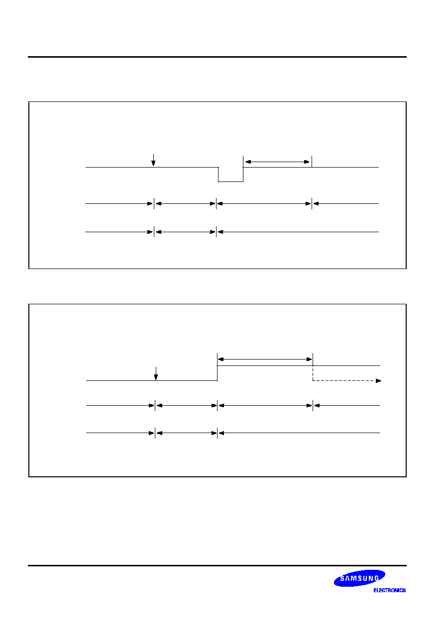
POWER-DOWN
KS57C0502/C0504/P0504 MICROCONTROLLER
84
STOP MODE TIMING DIAGRAMS
CLOCK
SIGNAL
STOP
INSTRUCTION
OSCILLATION
STABILIZATION
(31.3 ms / 4.19 MHz)
NORMAL MODE
IDLE MODE
NORMAL MODE
OSCILLATION RESUMES
STOP MODE
OSCILLATION
STOPS
RESET
Figure 83. Timing When Stop Mode is Released by
RESET
OSCILLATION
STABILIZATION
(BMOD SETTING)
NORMAL MODE
IDLE MODE
NORMAL MODE
OSCILLATION RESUMES
STOP MODE
OSCILLATION
STOPS
MODE
RELEASE
SIGNAL
STOP
INSTRUCTION
CLOCK
SIGNAL
INT ACK (IME = 1)
Figure 84. Timing When Stop Mode is Release by an Interrupt

KS57C0502/C0504/P0504 MICROCONTROLLER
POWER-DOWN
85
I/O PORT PIN CONFIGURATION FOR POWER-DOWN
The following method describes how to configure I/O port pins to reduce power consumption during power-
down modes (stop, idle):
Condition 1:
If the microcontroller is not configured to an external device:
1.
Connect unused port pins according to the information in Table 82.
2.
Disable all pull-up resistors for output pins by making the appropriate modifications to the pull-up resistor
mode register, PUMOD. Reason: If output goes low when the pull-up resistor is enabled, there may be un-
expected surges of current through the pull-up.
3.
Disable pull-up resistors for input pins configured to V
DD
or V
SS
levels in order to check the current input
option. Reason: If the input level of a port pin is set to V
SS
when a pull-up resistor is enabled, it will draw
an unnecessarily large current.
Condition 2:
If the microcontroller is configured to an external device and the external device's V
DD
source
is turned off in power-down mode.
1.
Connect unused port pins according to the information in Table 82.
2.
Disable the pull-up resistors of output pins by making the appropriate modifications to the pull-up resistor
mode register, PUMOD. Reason: If output goes low when the pull-up resistor is enabled, there may be un-
expected surges of current through the pull-up.
3.
Disable pull-up resistors for input pins configured to V
DD
or V
SS
levels in order to check the current input
option. Reason: If the input level of a port pin is set to V
SS
when a pull-up resistor is enabled, it will draw
an unnecessarily large current.
4.
Disable the pull-up resistors of input pins connected to the external device by making the necessary modi-
fications to the PUMOD register.
5.
Configure the output pins that are connected to the external device to low level. Reason: When the exter-
nal device's V
DD
source is turned off, and if the microcontroller's output pins are set to high level, V
DD
0.7 V is supplied to the V
DD
of the external device through its input pin. This causes the device to operate
at the level V
DD
0.7 V. In this case, total current consumption would not be reduced.
6.
Determine the correct output pin state necessary to block current pass in according with the external tran-
sistors (PNP, NPN).
POWER-DOWN
KS57C0502/C0504/P0504 MICROCONTROLLER
86
RECOMMENDED CONNECTIONS FOR UNUSED PINS
To reduce overall power consumption, please configure unused pins according to the guidelines described in
Table 82.
Table 82. Unused Pin Connections for Reduced Power Consumption
Pin/Share Pin Names
Recommended Connection
P0.0 /
SCK
P0.1 / SO
P0.2 / SI
Input mode: Connect to V
DD
Output mode: Do not connect
P1.0 / INT0 P1.1 / INT1
Connect to V
DD
P2.0 / CIN0
P2.1 / CIN1
P2.2 / CIN2
P2.3 / CIN3
Connect to V
DD
P3.0 / TCLO0
P3.1 / TCLO1
P3.2 / CLO
P3.3 / BUZ
P4.0P4.3
P5.0P5.3
P6.0 / KS0 P6.3 / BUZ
Input mode: Connect to V
DD
Output mode: Do not connect
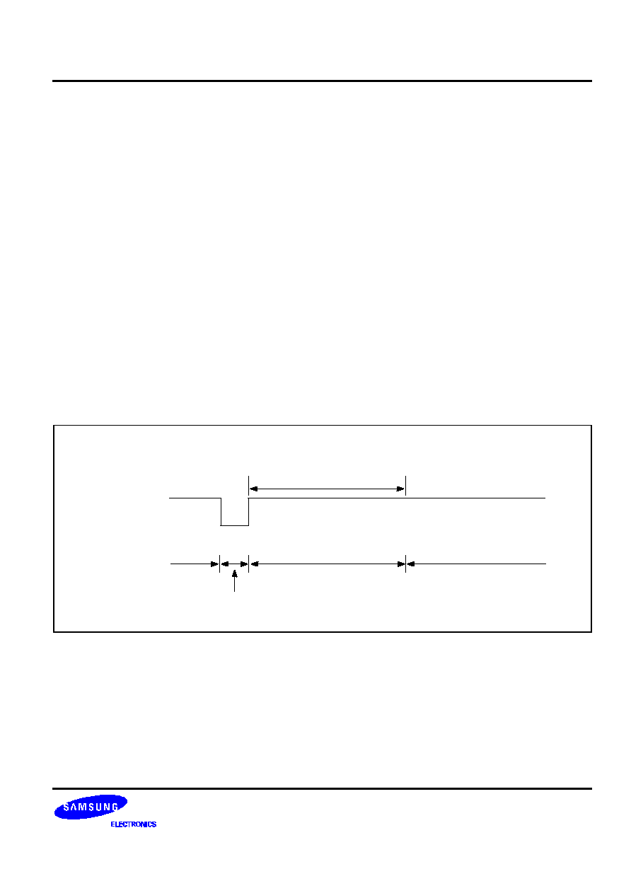
KS57C0502/C0504/P0504 MICROCONTROLLER
RESET
91
9
RESET
OVERVIEW
When a
RESET
signal is input during normal operation or power-down mode, a reset operation is initiated and
the CPU enters idle mode. Then, when the standard oscillation stabilization interval of 31.3 ms at 4.19 MHz has
elapsed, normal system operation resumes.
Regardless of when the
RESET
occurs -- during normal operating mode or during power-down mode -- the
effect on most hardware register values is almost identical. The exceptions are as follows:
-- Carry flag
-- Data memory values
-- General-purpose registers E, A, L, H, X, W, Z, and Y
-- Serial I/O buffer register (SBUF)
If a
RESET
occurs during idle or stop mode, the current values in these registers are retained. Otherwise, their
values are undefined.
OSCILLATION
STABILIZATION
(31.3 ms / 4.19 MHz)
IDLE MODE
OPERATING MODE
RESET
INPUT
NORMAL MODE
OR
POWER-DOWN
MODE
RESET OPERATION
Figure 91. Timing for Oscillation Stabilization After
RESET
HARDWARE REGISTER VALUES AFTER
RESET
Table 91 gives you detailed information about hardware register values after a
RESET
occurs during power-
down mode or during normal operation.
RESET
KS57C0502/C0504/P0504 MICROCONTROLLER
92
Table 9-1. Hardware Register Values After
RESET
Hardware Component
or Subcomponent
If
RESET
Occurs During
Power-Down Mode
If
RESET
Occurs During
Normal Operation
Program counter (PC)
Lower three bits of address 0000H
are transferred to PC11-8, and the
contents of 0001H to PC7-0.
Lower three bits of address 0000H
are transferred to PC11-8, and the
contents of 0001H to PC7-0.
Program Status Word (PSW):
Carry flag (C)
Retained
Undefined
Skip flag (SC0-SC2)
0
0
Interrupt status flags (IS0, IS1)
0
0
Bank enable flags (EMB, ERB)
Bit 6 of address 0000H in program
memory is transferred to the ERB
flag, and bit 7 of the address to
the EMB flag.
Bit 6 of address 0000H in program
memory is transferred to the ERB
flag, and bit 7 of the address to
the EMB flag.
Stack pointer (SP)
Undefined
Undefined
Data Memory (RAM):
General registers E, A, L, H, X, W, Z, Y
Values retained
Undefined
General-purpose registers
Values retained
(Note)
Undefined
Bank selection registers (SMB, SRB)
0, 0
0, 0
BSC register (BSC0-BSC3)
0
0
Clocks:
Power control register (PCON)
0
0
Clock output mode register (CLMOD)
0
0
Interrupts:
Interrupt request flags (IRQx)
0
0
Interrupt enable flags (IEx)
0
0
Interrupt priority flag (IPR)
0
0
Interrupt master enable flag (IME)
0
0
INT0 mode register (IMOD0)
0
0
INT1 mode register (IMOD1)
0
0
INTK mode register (IMODK)
0
0
NOTE:
The values of the 0F8H-0FDH are not retained when a
RESET
signal is input
KS57C0502/C0504/P0504 MICROCONTROLLER
RESET
93
Table 91. Hardware Register Values After
RESET
(Continued)
Hardware Component
or Subcomponent
If
RESET
Occurs During
Power-Down Mode
If
RESET
Occurs During
Normal Operation
I/O Ports:
Output buffers
Off
Off
Output latches
0
0
Port mode flags (PM)
0
0
Pull-up resistor mode reg (PUMOD)
0
0
Port 2 mode register (PWMOD)
0
0
Port open-drain enable register (PNE)
0
0
Watch-dog Timer:
WDT mode register (WDMOD)
A5H
A5H
WDT clear flag (WDTCF)
0
0
Basic Timer:
Count register (BCNT)
Undefined
Undefined
Mode register (BMOD)
0
0
Timer/Counter 0:
Count registers (TCNT0)
0
0
Reference registers (TREF0)
FFH, FFFFH
FFH, FFFFH
Mode registers (TMOD0)
0
0
Output enable flags (TOE0)
0
0
Watch Timer:
Watch timer mode register (WMOD)
0
0
Comparator
Comparator mode register (CMOD)
0
0
Comparison result register
Undefined
Undefined
Serial I/O Interface:
SIO mode register (SMOD)
0
0
SIO interface buffer (SBUF)
Values retained
Undefined

RESET
KS57C0502/C0504/P0504 MICROCONTROLLER
94
NOTES

KS57C0502/C0504/P0504 MICROCONTROLLER
I/O PORTS
101
10
I/O PORTS
OVERVIEW
The KS57C0502/C0504 has two input ports and five I/O ports. Pin addresses for all I/O ports are mapped to
locations FF0HFF6H in bank 15 of the RAM. The contents of I/O port pin latches can be read, written, or tested
at the corresponding address using bit manipulation instructions.
There are total of 6 input pins and 18 configurable I/O pin, including 8 high current I/O pins for a maximum
number of 24 I/O pins.
Port Mode Flags
Port mode flags (PM) are used to configure I/O ports 0 and 3 (port mode group 1), port 4 (port mode group 2),
and ports 5 and 6 (port mode group 3) to input or output mode by setting or clearing the corresponding I/O buffer.
PM flags are stored in three 8-bit registers in RAM area FE8HFEDH, and are addressable by 8-bit write
instructions only.
Port 2 Mode Register
Port 2 (P2.0P2.3) can be used as either for analog input or for digital input. P2MOD register settings
determines port 2 mode (analog or digital input) for specific port 2 pins.
Pull-Up Resistors
Pull-up resistors are assignable to input pins of ports 0, 1, 3, 4, 5 and 6. When a configurable I/O port pin
serves as an output pin, its assigned pull-up resistor is automatically disabled, even though the pin's pull-up
resistor is enabled by a corresponding bit setting in the pull-up resistor mode register (PUMOD).
PUMOD Control Register
The pull-up mode register (PUMOD) is an 8-bit register used to assign internal pull-up resistors by software to
specific I/O ports.
When a configurable I/O port pin is used as an output pin, its assigned pull-up resistor is automatically
disabled, even though the pin's pull-up is enabled by a corresponding PUMOD bit setting.
PUMOD is mapped to RAM address FDCHFDDH and is addressable by 8-bit write instructions only.
RESET
clears PUMOD register values to logic zero, automatically disconnecting all software-assignable port pull-up
resistors.
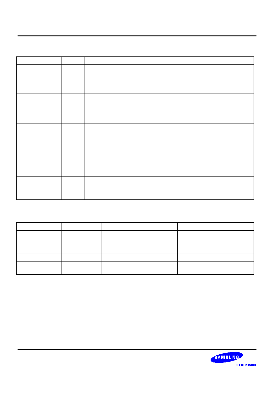
I/O PORTS
KS57C0502/C0504/P0504 MICROCONTROLLER
102
Table 101. I/O Port Overview
Port
I/O
Pins
Pin Names
Address
Function Description
0
I/O
3
P0.0P0.2
FF0H
3-bit I/O port.
1-bit and 3-bit read/write and test is possible.
Individual pins are software configurable as in-
put or output. 3-bit pull-up resistors are
assignable by software.
1
I
2
P1.0P1.1
FF1H
2-bit input port.
1-bit and 2-bit read and test is possible.
2-bit pull-up resistors are software assignable.
2
I
4
P2.0P2.3
FF2H
4-bit analog or digital input port.
1-bit or 4-bit read and test possible.
3
I/O
3
P3.0P3.2
FF3H
Same as port 0.
4, 5
I/O
8
P4.0P4.3
P5.0P5.3
FF4H
FF5H
4-bit I/O ports. 1-, 4-, and 8-bit read/write/test
is possible. Pins are individually configurable
as input or output. Ports 4 and 5 can be paired
to support 8-bit data transfer. 4-bit pull-up
registers are software assignable to input pins
and are automatically disabled for output pins.
The N-channel open drain or push-pull output
can be selected by software (1-bit unit)
6
I/O
4
P6.0P6.3
FF6H
4-bit I/O ports. Pins are individually software
configurable as input or output. 1-bit and 4-bit
read/write/test is possible. 4-bit pull-up
resistors are software assignable.
Table 102. I/O Port Pin Status During Instruction Execution
Instruction Type
Example
Input Mode Status
Output Mode Status
1-bit test
1-bit input
4-bit input
8-bit input
BTST
LDB
LD
LD
P0.1
C,P1.3
A,P6
EA,P4
Input or test data at each pin
Input or test data at output latch
1-bit output
BITR
P3.0
Output latch contents undefined
Output pin status is modified
4-bit output
8-bit output
LD
LD
P2,A
P6,EA
Transfer accumulator data to the
output latch
Transfer accumulator data to the
output pin
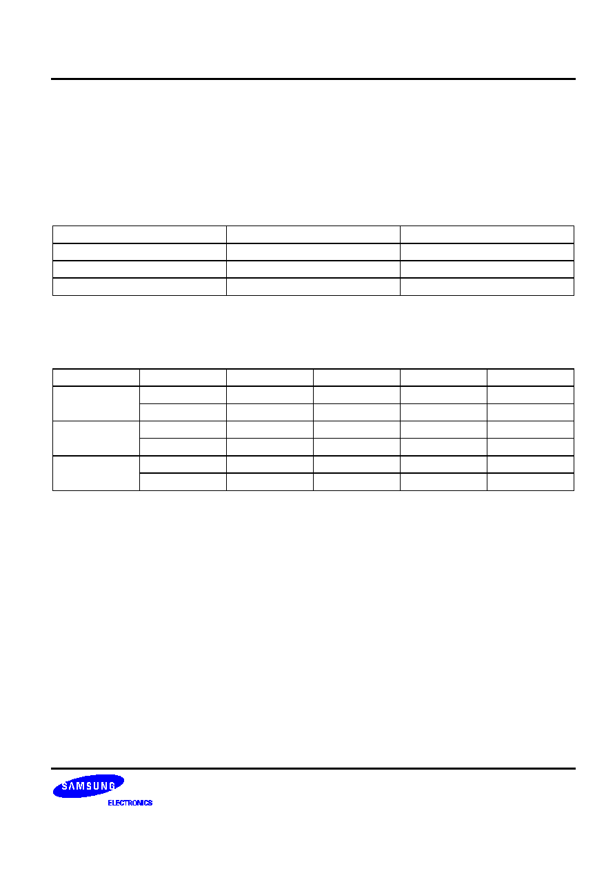
KS57C0502/C0504/P0504 MICROCONTROLLER
I/O PORTS
103
PORT MODE FLAGS (PM FLAGS)
Port mode flags (PM) are used to configure I/O ports 0 and 36 to input or output mode by setting or clearing
the corresponding I/O buffer. PM flags are stored in three 8-bit registers in RAM area FE8HFEDH, and are ad-
dressable by 8-bit write instructions only.
For convenient program reference, PM flags are organized into three groups -- PMG1, PMG2, and PMG3, as
shown in Table 103.
Table 103. Port Mode Groups and Corresponding I/O Ports
Port Mode Group ID
Corresponding I/O Ports
Port Mode Group Address
PMG1
Ports 0 and 3
FE8HFE9H
PMG2
Port 4
FEAHFEBH
PMG3
Ports 5 and 6
FECHFEDH
When a PM flag is "0", the port is set to input mode; when it is "1", the port is enabled for output.
RESET
clears
all port mode flags to logic zero, automatically configuring the corresponding I/O ports to input mode.
Table 104. Port Mode Flag Map
PM Group ID
Address
Bit 3
Bit 2
Bit 1
Bit 0
PMG1
FE8H
"0"
PM0.2
PM0.1
PM0.0
FE9H
"0"
PM3.2
PM3.1
PM3.0
PMG2
FEAH
PM4.3
PM4.2
PM4.1
PM4.0
FEBH
"0"
"0"
"0"
"0"
PMG3
FECH
PM5.3
PM5.2
PM5.1
PM5.0
FEDH
PM6.3
PM6.2
PM6.1
PM6.0
NOTE:
If bit = "0", the corresponding I/O pin is set to input mode. If bit = "1", the pin is set to output mode. All flags are
cleared to "0" following
RESET
.
+
+
PROGRAMMING TIP -- Configuring I/O Ports as Input or Output
Configure P0.0 and P3.0 as an output port and the other ports as input ports:
BITS
EMB
SMB
15
LD
EA,#11H
LD
PMG1,EA
;
P0.0 and P3.0
Output
LD
EA,#00H
LD
PMG2,EA
;
P4
Input
LD
EA,#00H
LD
PMG3,EA
;
P5, P6
Input
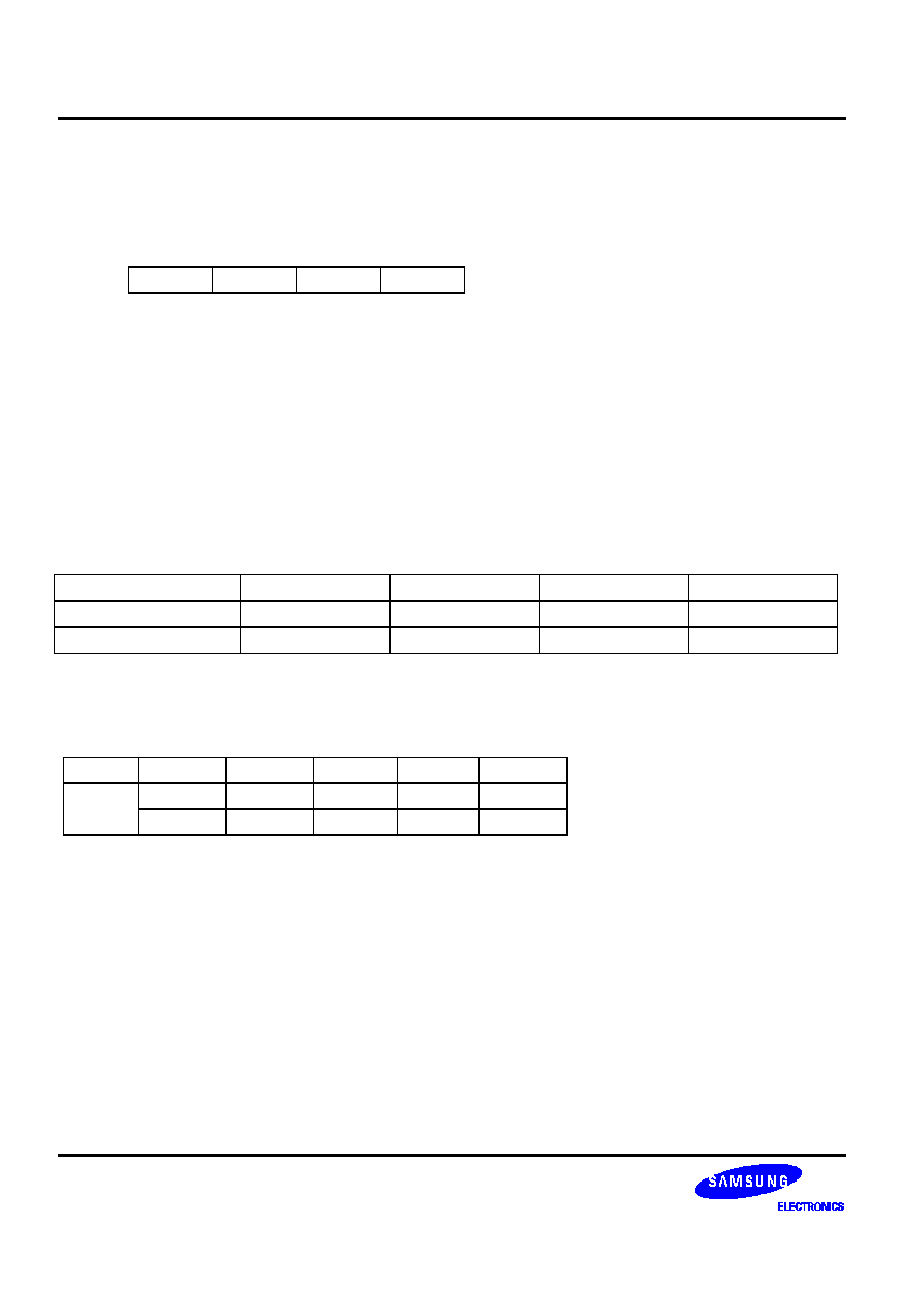
I/O PORTS
KS57C0502/C0504/P0504 MICROCONTROLLER
104
PORT 2 MODE REGISTER (P2MOD)
P2MOD register settings determine if port 2 is used either for analog input or for digital input. P2MOD register
is 4-bit write only register. P2MOD is mapped to address FE2H and initialized to zero by a
RESET
, configuring
port 2 as an analog input port.
FE2H
P2MOD.3
P2MOD.2
P2MOD.1
P2MOD.0
When bit is set to "1", the corresponding pin is configured as a digital input pin. When set to "0", configured as
an analog input pin: P2MOD.0 for P2.0, P2MOD.1 for P2.1, P2MOD.2 for P2.2, and P2MOD.3 for P2.3.
PULL-UP RESISTOR MODE REGISTER (PUMOD)
The pull-up resistor mode register (PUMOD) is an 8-bit register used to assign internal pull-up resistors by
software to specific I/O ports. When a configurable I/O port pin is used as an output pin, its assigned pull-up
resistor is automatically disabled, even though the pin's pull-up is enabled by a corresponding PUMOD bit
setting.
PUMOD is mapped to RAM address FDCHFDDH and is addressable by 8-bit write instructions only.
RESET
clears PUMOD register values to logic zero, automatically disconnecting all software-assignable port pull-up
resistors.
Table 105. Pull-Up Resistor Mode Register (PUMOD) Organization
Address
Bit 3
Bit 2
Bit 1
Bit 0
FDCH
PUMOD.3
"0"
PUMOD.1
PUMOD.0
FDDH
"0"
PUMOD.6
PUMOD.5
PUMOD.4
NOTE:
When bit = "1", a pull-up resistor is assigned to the corresponding I/O port: PUMOD.3 for port 3, PUMOD.6 for
port 6, and so on.
N-CHANNEL OPEN-DRAIN ENABLE REGISTER (PNE)
Address
Bit 3
Bit 2
Bit 1
Bit 0
PNE
FDAH
PNE4.3
PNE4.2
PNE4.1
PNE4.0
FDBH
PNE5.3
PNE5.2
PNE5.1
PNE5.0
The N-channel, open-drain mode register, PNE, is used to configure ports 4 and 5 to n-channel, open-drain
mode or as push-pull outputs.
When a bit in the PNE register is set to "1", the corresponding output pin is configured to n-channel, open-
drain; when set to "0", the output pin is configured to push-pull; PNE4.3 for P4.3, PNE4.2 for P4.2, PNE4.1 for
P4.1, PNE4.0 for P4.0, PNE5.3 for P5.3, PNE5.2 for P5.2, PNE5.1 for P5.1 and PNE5.0 for P5.0.
+
+
PROGRAMMING TIP -- Enabling and Disabling I/O Port Pull-Up Resistors
P6 enable pull-up resistors, P0, P1, P3, P4 and P5 disable pull-up resistors.
BITS
EMB
SMB
15
LD
EA,#40H
LD
PUMOD,EA
;
P6 enable
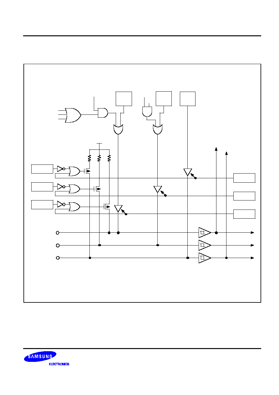
KS57C0502/C0504/P0504 MICROCONTROLLER
I/O PORTS
105
PORT 0 CIRCUIT DIAGRAM
SCK
SCK
SO
SI
P0.2
LATCH
P0.1
LATCH
P0.0
LATCH
PM0.2
PM0.1
PM0.0
V
DD
When a port pin acts as an output, its pull-up resistor is automatically disabled,
even though the port's pull-up resistor is enabled by bit settings to the pull-up
resistor mode register (PUMOD).
NOTE:
P0.0 /
SCK
SMOD.7
SMOD.6
SMOD.5
SMOD.1
PUMOD.0
PUMOD.0
PUMOD.0
P0.1 / SO
P0.2 / SI
Figure 101. I/O Port 0 Circuit Diagram
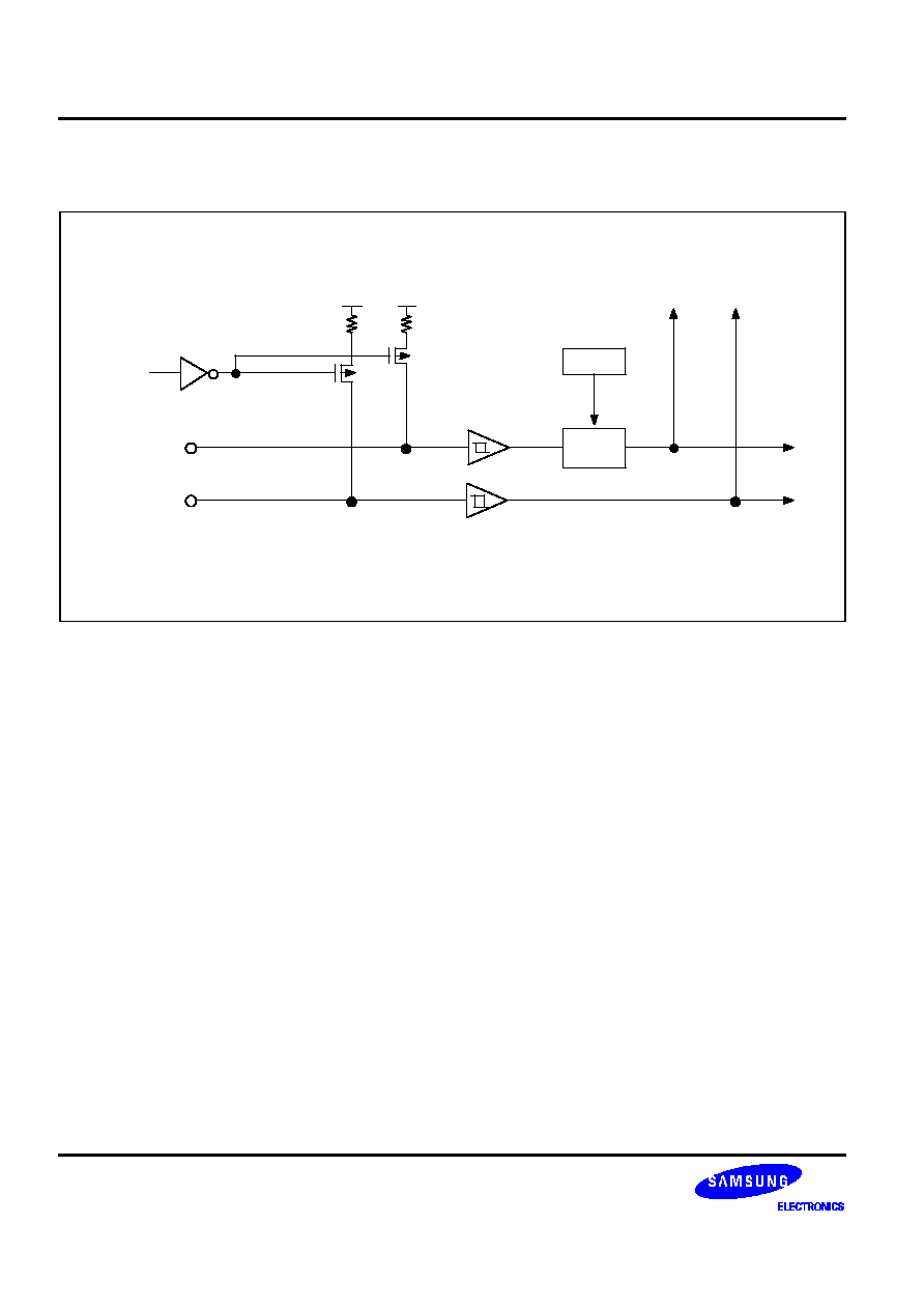
I/O PORTS
KS57C0502/C0504/P0504 MICROCONTROLLER
106
PORT 1 CIRCUIT DIAGRAM
INT0
INT1
P1.0 / INT0
PUMOD.1
P1.1 / INT1
V
DD
V
DD
N/R
Circuit
N/R = Noise reduction
IMOD0
Figure 102. Input Port 1 Circuit Diagram
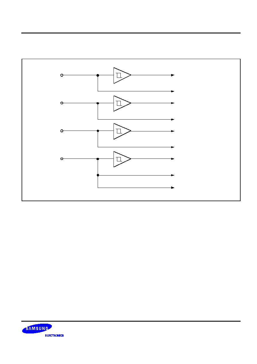
KS57C0502/C0504/P0504 MICROCONTROLLER
I/O PORTS
107
PORT 2 CIRCUIT DIAGRAM
P2.0 / CIN0
P2.1 / CIN1
P2.2 / CIN2
P2.3 / CIN3
ANALOG INPUT
DIGITAL INPUT
ANALOG INPUT
ANALOG INPUT
ANALOG INPUT
DIGITAL INPUT
DIGITAL INPUT
DIGITAL INPUT
EXTERNAL REFERENCE
Figure 103. Port 2 Circuit Diagram
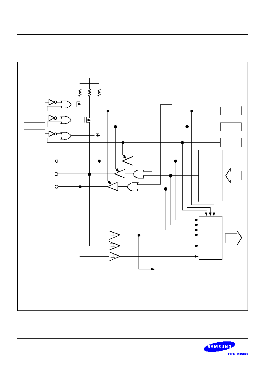
I/O PORTS
KS57C0502/C0504/P0504 MICROCONTROLLER
108
PORT 3 CIRCUIT DIAGRAM
PM3.2
PM3.1
PM3.0
V
DD
PUMOD.3
PUMOD.3
PUMOD.3
When a port pin acts as an output, its pull-up resistor is automatically disabled,
even though the port's pull-up resistor is enabled by bit settings to the pull-up
resistor mode register (PUMOD).
NOTE:
1, 4
TCL0
TC0 CLOCK OUTPUT
CLOCK OUTPUT
P3.0 / TCL0
P3.1 / TCLO0
P3.2 / CLO
OUTPUT
LATCH
1, 4
M
U
X
Figure 104. Port 3 Circuit Diagram
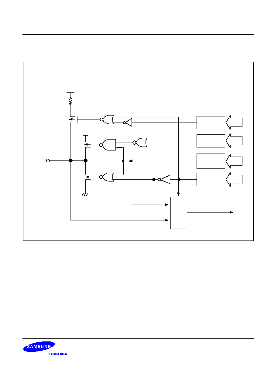
KS57C0502/C0504/P0504 MICROCONTROLLER
I/O PORTS
109
PORTS 4 AND 5 CIRCUIT DIAGRAM
Px.b
V
DD
1, 4, 8
8
P-CH
N-CH
V
SS
M
U
X
P-CH
PUMOD.b
b=4, 5
OUTPUT
LATCH
PNE
PMx.b
x=4, 5
b=0, 1, 2, 3
8
8
Figure 105. Circuit Diagram for Ports 4 and 5
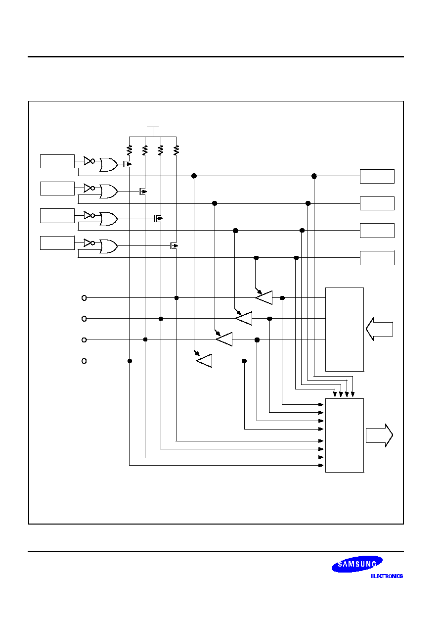
I/O PORTS
KS57C0502/C0504/P0504 MICROCONTROLLER
1010
PORT 6 CIRCUIT DIAGRAM
P6.0 / KS0
P6.1 / KS1
P6.2 / KS2
P6.3 / BUZ
V
DD
When a port pin acts as an output, its pull-up resistor is automatically disabled,
even though the port's pull-up resistor is enabled by bit settings to the pull-up
resistor mode register (PUMOD).
NOTE:
1, 4
1, 4
OUTPUT
LATCH
PM6.2
PM6.3
PM6.1
PUMOD.6
PUMOD.6
PUMOD.6
PUMOD.6
PM6.0
M
U
X
Figure 106. Port 6 Circuit Diagram

KS57C0502/C0504/P0504 MICROCONTROLLER
TIMERS and TIMER/COUNTER
111
11
TIMERS and TIMER/COUNTER
OVERVIEW
There are three timer and timer/counter function modules:
-- 8-bit basic timer (BT)
-- 8-bit timer/counter 0 (TC0)
-- Watch timer (WT)
The 8-bit basic timer (BT) is the microcontroller's main interval timer. It generates a interrupt request at a fixed
time interval by making the appropriate modification to the mode register.
The basic timer also functions as a 'watchdog' timer and is used to determine clock oscillation stabilization
time when stop mode is released by an interrupt and after a
RESET
.
The 8-bit timer/counter 0 (TC0) is programmable timer/counter that is used primarily for event counting and for
clock frequency modification and output. In addition, TC0 generates a clock signal that can be used by the serial
I/O interface.
The watch timer (WT) module consists of an 8-bit watch timer mode register, a clock selector, and a frequency
divider circuit. Watch timer functions include real-time and watch-time measurement, system clock interval
timing, and generation of buzzer output.

TIMERS and TIMER/COUNTER
KS57C0502/C0504/P0504 MICROCONTROLLER
112
BASIC TIMER (BT)
OVERVIEW
The 8-bit basic timer (BT) has four functional components:
-- Clock selector logic
-- 4-bit mode register (BMOD)
-- 8-bit counter register (BCNT)
The basic timer generates interrupt requests at precise intervals, based on the frequency of the system clock.
You can use the basic timer as a "watchdog" timer for monitoring system events or use BT output to stabilize
clock oscillation when stop mode is released by an interrupt and following
RESET
.
Use the basic timer mode register, BMOD, to turn the BT on and off, to select input clock frequency, and to
control interrupt or stabilization intervals.
Interval Timer Function
The measurement of elapsed time intervals is the basic timer's primary function. The standard interval is 256
BT clock pulses.
To restart the basic timer, set bit 3 of the mode register BMOD to logic one. The input clock frequency and the
interrupt and stabilization interval are selected by loading the appropriate bit values to BMOD.2BMOD.0.
The 8-bit counter register, BCNT, is incremented each time a clock signal is detected that corresponds to the
frequency selected by BMOD. BCNT continues incrementing as it counts BT clocks until an overflow occurs.
An overflow causes the BT interrupt request flag (IRQB) to be set to logic one to signal that the designated
time interval has elapsed. An interrupt request is then generated, BCNT is cleared to logic zero, and counting
continues from 00H.
Watchdog Timer Function
The basic timer can also be used as a "watch-dog" timer to detects inadvertent program loop, that is, system
or program operation error. For this purpose, instruction that clear the watch-dog timer(BITS WDTCF) should
be executed at proper points in a program within a given period. If an instruction that clears the watch-dog timer
is not executed within the period and the watch-dog timer overflows, reset signal is generated and system is
restarted with reset status. An operation of watch-dog timer is as follows:
Write some value(except #5AH) to Watch-Dog Timer Mode register, WDMOD.
If WDCNT overflows, system reset is generated.
Oscillation Stabilization Interval Control
Bits 20 of the BMOD register are used to select the input clock frequency for the basic timer. This setting also
determines the time interval (also referred to as 'wait time') required to stabilize clock signal oscillation when
power-down mode is released by an interrupt. When a
RESET signal is generated
, the standard stabilization interval
for system clock oscillation following a
RESET
is 31.3 ms at 4.19 MHz.
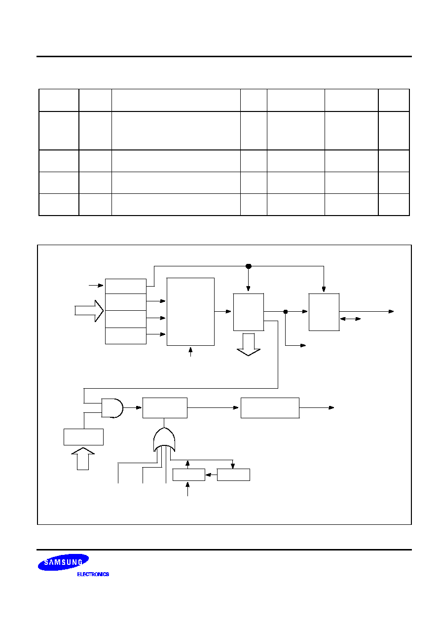
KS57C0502/C0504/P0504 MICROCONTROLLER
TIMERS and TIMER/COUNTER
113
Table 111. Basic Timer Register Overview
Register
Name
Type
Description
Size
RAM
Address
Addressing
Mode
Reset
Value
BMOD
Control
Controls the clock frequency (mode)
of the basic timer; also, the
oscillation stabilization interval after
power-down mode release or
RESET
4-bit
F85H
4-bit write-
only;
BMOD.3: also
1-bit writeable
"0"
BCNT
Counter Counts clock pulses matching the
BMOD frequency setting
8-bit
F86H - F87H
8-bit
read-only
U
*
WDMOD
Control
Controls watch-dog timer operation.
8-bit
F98H
Ä
F99H
8-bit write-
only
A5H
WDTCF
Control
Clear the watch-dog timer's counter.
1-bit
F9AH.3
1-bit write-
only
"0"
*
'U' means the value is undetermined after a
RESET
.
"CLEAR" SIGNAL
BITS
INSTRUCTION
CLOCK
SELECTOR
BCNT
IRQB
INTERRUPT
REQUEST
OVERFLOW
CPU CLOCK
START SIGNAL
(POWER-DOWN RELEASE)
1-BIT R/W
CLOCK INPUT
CLEAR
IRQB
4
CLEAR
BCNT
8
BMOD.3
BMOD.2
BMOD.1
BMOD.0
WDMOD
WDTCNT
RESET
GENERATION
8
WDTCF
DELAY
WAIT* RESET STOP
BITS
INSTRUCTION
*WAIT means
-Stabilization time after RESET
- Stabilization time after STOP mode release
1 pulse period=BT input clock 2
8
(1/2 duty)
RESET
OVERFLOW
CLEAR
3-BIT COUNTER
Figure 111. Basic Timer Circuit Diagram
TIMERS and TIMER/COUNTER
KS57C0502/C0504/P0504 MICROCONTROLLER
114
BASIC TIMER MODE REGISTER (BMOD)
The basic timer mode register, BMOD, is a 4-bit write-only register located at RAM address F85H. Bit 3, the
basic timer start control bit, is also 1-bit addressable. All BMOD values are set to logic zero following
RESET
and
interrupt request signal generation is set to the longest interval. (BT counter operation cannot be stopped.)
BMOD settings have the following effects:
-- Restart the basic timer,
-- Control the frequency of clock signal input to the basic timer, and
-- Determine time interval required for clock oscillation to stabilize following the release of stop modes by an
interrupt.
By loading different values into the BMOD register, you can dynamically modify the basic timer clock
frequency during program execution. Four BT frequencies, ranging from fx/2
12
(1.02 kHz) to fx/2
5
(131 kHz), are
selectable. Since BMOD's reset value is logic zero, the default clock frequency setting is fx/2
12
. (kHz frequencies
assume a system clock (fx) frequency of 4.19 MHz.)
The most significant bit of the BMOD register, BMOD.3, is used to start the basic timer again. When BMOD.3
is set to logic one (enabled) by a 1-bit write instruction, the contents of the BT counter register (BCNT) and the
BT interrupt request flag (IRQB) are both cleared to logic zero, and timer operation is restarted.
The combination of bit settings in the remaining three registers -- BMOD.2, BMOD.1, and BMOD.0 --
determine the clock input frequency and oscillation stabilization interval.
Table 112. Basic Timer Mode Register (BMOD) Organization
BMOD.3
Basic Timer Enable/Disable Control Bit
1
Start basic timer; clear IRQB, BCNT, and BMOD.3 to "0"
BMOD.2
BMOD.1
BMOD.0
Basic Timer Input Clock
Oscillation Stabilization
0
0
0
fx/2
12
(1.02 kHz)
2
20
/fx (250 ms)
0
1
1
fx/2
9
(8.18 kHz)
2
17
/fx (31.3 ms)
1
0
1
fx/2
7
(32.7 kHz)
2
15
/fx (7.82 ms)
1
1
1
fx/2
5
(131 kHz)
2
13
/fx (1.95 ms)
NOTES:
1.
Clock frequencies and stabilization intervals assume a system oscillator clock frequency (fx) of 4.19 MHz.
2.
fx = system clock frequency.
3.
Oscillation stabilization time is the time required to stabilize clock signal oscillation after stop mode is released.
4.
The standard stabilization time for system clock oscillation following a
RESET
is 31.3 ms at 4.19 MHz.

KS57C0502/C0504/P0504 MICROCONTROLLER
TIMERS and TIMER/COUNTER
115
BASIC TIMER COUNTER (BCNT)
BCNT is an 8-bit counter register for the basic timer. It is mapped to RAM addresses F86HF87H and can be
addressed by 8-bit read instructions.
RESET
leaves the BCNT register value undetermined. BCNT is automatically cleared to logic zero whenever
the BMOD register control bit (BMOD.3) is set to "1" to restart the basic timer. It is incremented each time a clock
pulse of the frequency determined by the current BMOD bit settings is detected.
When BCNT has incremented to hexadecimal 'FFH' (256 clock pulses), it is cleared to '00H' and an overflow
is generated. The overflow causes the interrupt request flag, IRQB, to be set to logic one. When the interrupt
request is generated, BCNT immediately resumes counting incoming clock signals.
NOTE
Always execute a BCNT read operation twice to eliminate the possibility of reading unstable data
while the counter is incrementing. If, after two consecutive reads, the BCNT values match, you can
select the latter value as valid data. Until the results of the consecutive reads match, however, the
read operation must be repeated until the validation condition is met.
BASIC TIMER OPERATION SEQUENCE
The basic timer's sequence of operations may be summarized as follows:
1.
Set bit BMOD.3 to logic one to restart basic timer operation
2.
BCNT is incremented by one after each clock pulse corresponding to BMOD selection
3.
BCNT overflows if BCNT
255 (FFH)
4.
When an overflow occurs, the IRQB flag is set to logic one by hardware
5.
The interrupt request is generated
6.
BCNT is automatically cleared to logic zero (BCNT = 00H)
7.
BCNT resumes counting BT clock pulse
TIMERS and TIMER/COUNTER
KS57C0502/C0504/P0504 MICROCONTROLLER
116
+
+
PROGRAMMING TIP -- Using the Basic Timer
1.
To read the basic timer count register (BCNT):
BITS
EMB
SMB
15
BCNTR
LD
EA,BCNT
LD
YZ,EA
LD
EA,BCNT
CPSE
EA,YZ
JR
BCNTR
2.
When stop mode is released by an interrupt, set the oscillation stabilization interval to 31.3 ms:
BITS
EMB
SMB
15
LD
A,#0BH
LD
BMOD,A
;
Wait time is 31.3 ms
STOP
;
Set stop power-down mode
NOP
NOP
NOP
NORMAL
OPERATING MODE
STOP MODE
IDLE MODE
(31.3 ms)
CPU
OPERATION
STOP
INSTRUCTION
STOP MODE IS
RELEASED BY
INTERRUPT
NORMAL
OPERATING MODE
3.
To set the basic timer interrupt interval time to 1.95 ms (at 4.19 MHz):
BITS
EMB
SMB
15
LD
A,#0FH
LD
BMOD,A
EI
BITS
IEB
;
Basic timer interrupt enable flag is set to "1"
4.
Clear BCNT and the IRQB flag and restart the basic timer:
BITS
EMB
SMB
15
BITS
BMOD.3
KS57C0502/C0504/P0504 MICROCONTROLLER
TIMERS and TIMER/COUNTER
117
WATCH-DOG TIMER MODE REGISTER (WDMOD)
The watch-dog timer mode register, WDMOD, is a 8-bit write-only register located at RAM address F98H -
F99H. WDMOD register controls to enable or disable the watch-dog timer function. WDMOD values are set to
logic "A5H" following
RESET
and this value enable the watch-dog timer, and watch-dog time
r's
period is set to the longest
interval because
BT
overflow signal is
generated with the longest interval. (BT counter operation cannot be stopped.)
WDMOD - WatchDog Timer Mode Control Register
F99H,F98H
Bit
3
2
1
0
3
2
1
0
Identifier
.7
.6
.5
.4
.3
.2
.1
.0
RESET
Value
1
0
1
0
0
1
0
1
Read/Write
W
W
W
W
W
W
W
W
WDMOD
Watch-Dog Timer Enable/Disable Control
5AH
Disable Watch-dog timer function
Any other Value
Enable Watch-dog timer function
WATCH-DOG TIMER COUNTER (WDCNT)
WDCNT is an 3-bit counter. WDCNT is automatically cleared to logic zero whenever the WDTCF register
control bit (WDTCF) is set to "1" to restart the WDCNT. Reset, stop, and wait signal clear the WDCNT to logic
zero also. WDCNT is incremented each time a clock pulse of the overflow frequency determined by the current
BMOD bit settings. When WDCNT has incremented to hexadecimal '07H' (8 BT overflow pulses), it is cleared to
'00H' and an overflow is generated. The overflow causes the system reset. When the interrupt request is
generated, BCNT immediately resumes counting incoming clock signals.
WATCH-DOG TIMER'S COUNTER CLEAR FLAG(WDTCF)
WDTCF(F9AH.3) setting clear the WDT's counter to zero and restart the WDT's counter.
Table 11-3. Watch-Dog Timer Interval Time
BMOD
BT Input Clock
WDCNT input clock
WDT interval time
Main clock
x000b
2
12
/fx
2
12
/fx
×
2
8
2
12
/fx
×
2
8
×
2
3
2 sec
x011b
2
9
/fx
2
9
/fx
×
2
8
2
9
/fx
×
2
8
×
2
3
250 msec
x101b
2
7
/fx
2
7
/fx
×
2
8
2
7
/fx
×
2
8
×
2
3
62.5 msec
x111b
2
5
/fx
2
5
/fx
×
2
8
2
5
/fx
×
2
8
×
2
3
15.6 msec
NOTES:
1.
Clock frequencies assume a system oscillator clock frequency (fx) of : Main clock 4.19MHz
2. fx = system clock frequency.

TIMERS and TIMER/COUNTER
KS57C0502/C0504/P0504 MICROCONTROLLER
118
8-BIT TIMER/COUNTER 0 (TC0)
Timer/counter 0 (TC0) is used to count system 'events' by identifying the transition (high-to-low or low-to-high)
of incoming square wave signals. To indicate that an event has occurred, or that a specified time interval has
elapsed, TC0 generates an interrupt request. By counting signal transitions and comparing the current counter
value with the reference register value, TC0 can be used to measure specific time intervals.
TC0 has a reloadable counter that consists of two parts: an 8-bit reference register (TREF0) into which you
write the counter reference value, and an 8-bit counter register (TCNT0) whose value is automatically
incremented by counter logic.
An 8-bit mode register, TMOD0, is used to activate the timer/counter and to select the basic clock frequency to
be used for timer/counter operations. You can modify the basic frequency dynamically by loading new values into
TMOD0 during program execution.
TC0 FUNCTION SUMMARY
8-bit programmable timer
Generates interrupts at specific time intervals based on the selected clock fre-
quency.
External event counter
Counts various system "events" based on edge detection of external clock sig-
nals at the TC0 input pin, TCL0. To start the event counting operation,
TMOD0.2 is set to "1" and TMOD0.6 is cleared to "0".
Arbitrary frequency output
Outputs selectable clock frequencies to the TC0 output pin, TCLO0.
External signal divider
Divides the frequency of an incoming external clock signal according to a
modifiable reference value (TREF0), and outputs the modified frequency to the
TCLO0 pin.
Serial I/O clock source
Outputs a modifiable clock signal for use as the
SCK
clock source.
KS57C0502/C0504/P0504 MICROCONTROLLER
TIMERS and TIMER/COUNTER
119
TC0 COMPONENT SUMMARY
Mode register (TMOD0)
Activates the timer/counter and selects the internal clock frequency or the
external clock source at the TCL0 pin.
Reference register (TREF0)
Stores the reference value for the desired number of clock pulses between in-
terrupt requests.
Counter register (TCNT0)
Counts internal or external clock pulses based on the bit settings in TMOD0
and TREF0.
Clock selector circuit
Together with the mode register (TMOD0), lets you select one of four internal
clock frequencies, or external clock frequency.
8-bit comparator
Determines when to generate an interrupt by comparing the current value of
the counter register (TCNT0) with the reference value previously programmed
into the reference register (TREF0).
Output latch (TOL0)
Where a TC0 interrupt request or clock pulse is stored pending output to the
serial I/O circuit or to the TC0 output pin, TCLO0.
When the contents of the TCNT0 and TREF0 registers coincide, the
timer/counter interrupt request flag (IRQT0) is set to "1", the status of TOL0 is
inverted, and an interrupt is generated.
Output enable flag (TOE0)
You must set this flag to logic one before the contents of the TOL0 latch can
be output to TCLO0.
Interrupt request flag (IRQT0)
This flag is cleared when TC0 operation starts and the TC0 interrupt service
routine is executed and is enabled whenever the counter value and reference
value coincide.
Interrupt enable flag (IET0)
Must be set to logic one before the interrupt requests generated by
timer/counter can be processed.
Table 114. TC0 Register Overview
Register
Name
Type
Description
Size
RAM
Address
Addressing
Mode
Reset
Value
TMOD0
Control
Controls TC0 restart (bit 2);
clears and resumes counting
operation (bit 3); sets input
clock and clock frequency (bits
64)
8-bit
F90HF91H
8-bit write-
only;
(TMOD0.3 is
also 1-bit
write-only)
"0"
TCNT0
Counter
Counts clock pulses matching
the TMOD0 frequency setting
8-bit
F94HF95H
8-bit
read-only
"0"
TREF0
Reference
Stores reference value for the
timer/counter 0 interval setting
8-bit
F96HF97H
8-bit
write-only
FFH
TOE0
Flag
Controls timer/counter 0 output
to the TCLO0 pin
1-bit
F92H.2
1-bit
write-only
"0"
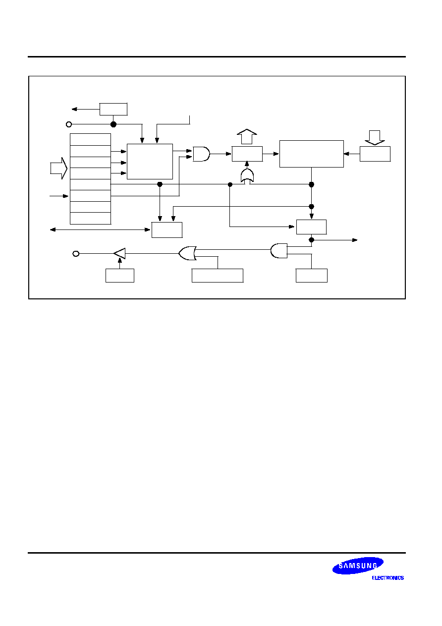
TIMERS and TIMER/COUNTER
KS57C0502/C0504/P0504 MICROCONTROLLER
1110
TCL0
TCLO0
SERIAL
I/O
TCNT0
CLEAR
INVERTED
CLEAR
SET
CLEAR
CLOCKS
(fx/2 , fx/2 , fx/2 , fx)
10
6
4
8
8
CLOCK
SELECTOR
8-BIT
COMPARATOR
P3.0
TOL0
P3.1 LATCH
TOE0
IRQT0
PM3.1
TMOD0.7
TMOD0.6
TMOD0.5
TMOD0.4
TMOD0.3
TMOD0.2
TMOD0.1
TMOD0.0
TREF0
8
Figure 112. TC0 Circuit Diagram
TC0 ENABLE/DISABLE PROCEDURE
Enable Timer/Counter 0
--
Set TMOD.2 to logic one (RAM address F90H.2)
--
Set the TC0 interrupt enable flag IET0 to logic one (RAM address FBCH.1)
--
Set TMOD0.3 to logic one (RAM address F90H.3)
TCNT0, IRQT0, and TOL0 are cleared to logic zero, and timer/counter operation starts.
Disable Timer/Counter
--
Set TMOD0.2 to logic zero (RAM address F90H.2)
Clock signal input to the counter register TCNT0 is halted. The current TCNT0 value is retained and can be read
if necessary.

KS57C0502/C0504/P0504 MICROCONTROLLER
TIMERS and TIMER/COUNTER
1111
TC0 PROGRAMMABLE TIMER/COUNTER FUNCTION
Timer/counter 0 can be programmed to generate interrupt requests at various intervals, based on the system
clock frequency you select.
The 8-bit TC0 mode register, TMOD0, is used to activate the timer/counter and to select the clock frequency.
The reference register, TREF0, stores your value for the number of clock pulses to be generated between inter-
rupt requests. The counter register, TCNT0, counts the incoming clock pulses, which are compared to the TREF0
value as TCNT0 is incremented. When there is a match (TREF0 = TCNT0), an interrupt request is generated.
To program timer/counter to generate interrupt requests at specific intervals, you choose one of four internal
clock frequencies (divisions of the system clock, fx) and load your own counter reference value into the TREF0
register.
TCNT0 is incremented each time an internal counter pulse is detected with the reference clock frequency
specified by TMOD0.4TMOD0.6 settings. To generate an interrupt request, the TC0 interrupt request flag
(IRQT0) is set to logic one, the status of TOL0 is inverted, and the interrupt is generated. The content of TCNT0
is then cleared to 00H, and TC0 continues counting.
The interrupt request mechanism for the programmable timer/counter consists of the TC0 interrupt enable flag
IET0 and the TC0 interrupt request flag IRQT0.
TC0 OPERATION SEQUENCE
The general sequence of operations when using TC0 as a programmable timer/counter can be summarized as
follows:
1.
Set TMOD0.2 to "1" to enable TC0
2.
Set TMOD0.6 to "1" to enable the system clock (fx) input
3.
Set TMOD0.5 and TMOD0.4 bits to desired internal frequency (fx/2n)
4.
Load a value to TREF0 to specify the interval between interrupt requests
5.
Set the TC0 interrupt enable flag (IET0) to "1"
6.
Set TMOD0.3 bit to "1" to clear TCNT0, IRQT0, and TOL0, and start counting
7.
TCNT0 increments with each internal clock pulse
8.
When the comparator shows TCNT0 = TREF0, the IRQT0 flag is set to "1"
9.
Output latch (TOL0) logic toggles high or low
10.
Interrupt request is generated
11.
TCNT0 is cleared to 00H and counting resumes
12.
Programmable timer/counter operation continues until TMOD0.2 is cleared to "0".
TIMERS and TIMER/COUNTER
KS57C0502/C0504/P0504 MICROCONTROLLER
1112
TC0 EVENT COUNTER FUNCTION
Timer/counter 0 can be used to monitor or detect system 'events' by using the external clock input at the TCL0
pin (I/O port 3.0) as the counter source. The TC0 mode register is used to specify rising or falling edge detection
for incoming clock signals. The counter register TCNT0 is incremented each time the selected state transition of
the external clock signal occurs. To activate the TC0 event counter function,
-- Set TMOD0.2 to "1" to enable TC0
-- Clear TMOD0.6 to "0" to select the external clock source at the TCL0 pin
-- Select TCL0 edge detection for rising or falling signal edges by loading the appropriate values to TMOD0.5
and TMOD0.4.
-- P3.0 must be set to input mode.
Table 115. TMOD0 Settings for TCL0 Edge Detection
TMOD0.5
TMOD0.4
TCL0 Edge Detection
0
0
Rising edges
0
1
Falling edges
With the exception of the different TMOD0.4TMOD0.6 settings, the operation sequence for TC's event
counter function is identical to its programmable counter/timer function.

KS57C0502/C0504/P0504 MICROCONTROLLER
TIMERS and TIMER/COUNTER
1113
TC0 CLOCK FREQUENCY OUTPUT
Using timer/counter, you can output a modifiable clock frequency to the TC0 clock output pin, TCLO0. To
select the clock frequency, you load appropriate values to the TC0 mode register, TMOD0. The clock interval is
determined by loading the desired reference value into the reference register TREF0. Then, to enable the output
to the TCLO0 pin at I/O port 3.1, the following conditions must be met:
-- TC0 output enable flag TOE0 must be set to "1"
-- I/O mode flag for P3.1 (PM3.1) must be set to output mode ("1")
-- Output latch value for P3.1 must be set to "0"
In summary, the operational sequence required to output a TC0-generated clock signal to the TCLO0 pin is as
follows:
1.
Load your reference value to TREF0
2.
Set the clock frequency in TMOD0
3.
Initiate TC0 clock output to TCLO0 (TMOD0.2 = "1")
4.
Set port 3 mode flag (PM3.1) to "1"
5.
Set P3.1 output latch to "0"
6.
Set TOE0 flag to "1"
Each time TCNT0 overflows and an interrupt request is generated, the state of the output latch TOL0 is in-
verted and the TC0-generated clock signal is output to the TCLO0 pin.
+
+
PROGRAMMING TIPS -- TC0 Signal Output to the TCLO0 Pin
Output a 30 ms pulse width signal to the TCLO0 pin:
BITS
EMB
SMB
15
LD
EA,#79H
LD
TREF0,EA
LD
EA,#4CH
LD
TMOD0,EA
LD
EA,#20H
LD
PMG1,EA
;
P3.1
Output mode
BITR
P3.1
;
P3.1 clear
BITS
TOE0
TIMERS and TIMER/COUNTER
KS57C0502/C0504/P0504 MICROCONTROLLER
1114
TC0 SERIAL I/O CLOCK GENERATION
Timer/counter 0 can supply a clock signal to the clock selector circuit of the serial I/O interface for data shifter
and clock counter operations. (These internal SIO operations are controlled in turn by the SIO mode register,
SMOD). This clock generation function enables you to adjust data transmission rates across the serial interface.
Use TMOD0 and TREF0 register settings to select the frequency and interval of the TC0 clock signals to be
used as
SCK
input to the serial interface. The generated clock signal is then sent directly to the serial I/O clock
selector circuit -- not through the port 3.1 latch and TCLO0 pin.
TC0 EXTERNAL INPUT SIGNAL DIVIDER
By selecting an external clock source and loading a reference value into the TC0 reference register, TREF0,
you can divide the incoming clock signal by the TREF0 value and then output this modified clock frequency to
the TCLO0 pin. The sequence of operations used to divide external clock input may be summarized as follows:
1.
Load a signal divider value to the TREF0 buffer register
2.
Clear TMOD0.6 to "0" to enable external clock input at the TCL0 pin
3.
Set TMOD0.5 and TMOD0.4 to desired TCL0 signal edge detection
4.
Set port 3.1 mode flag (PM3.1) to output ("1")
5.
Set P3.1 output latch to "0"
6.
Set TOE0 flag to "1" to enable output of the divided frequency
Divided clock signals are then output to the TCLO0 pin.
+
+
PROGRAMMING TIP -- External TCL0 Clock Output to the TCLO0 Pin
Output external TCL0 clock pulse to the TCLO0 pin (divide by four):
EXTERNAL (TCL0)
CLOCK PULSE
TCLO0
OUTPUT
PULSE
BITS
EMB
SMB
15
LD
EA,#01H
LD
TREF0,EA
LD
EA,#0CH
LD
TMOD0,EA
LD
EA,#20H
LD
PMG1,EA
;
P3.1
Output mode
BITR
P3.1
;
P3.1 clear
BITS
TOE0
KS57C0502/C0504/P0504 MICROCONTROLLER
TIMERS and TIMER/COUNTER
1115
TC0 MODE REGISTER (TMOD0)
TMOD0 is the 8-bit mode control register for timer/counter. It is located at RAM addresses F90HF91H and is
addressable by 8-bit write instructions. One bit, TMOD0.3, is also 1-bit writeable.
RESET
clears all TMOD0 bits to
logic zero and disables TC0 operations.
F90H
TMOD0.3
TMOD0.2
"0"
"0"
F91H
"0"
TMOD0.6
TMOD0.5
TMOD0.4
TMOD0.2 is the enable/disable bit for timer/counter. When TMOD0.3 is set to "1", the contents of TCNT0,
IRQT0, and TOL0 are cleared, counting starts from 00H, and TMOD0.3 is automatically reset to "0" for normal
TC0 operation. When TC0 operation stops (TMOD0.2 = "0"), the contents of the TC0 counter register, TCNT0,
are retained until TC0 is re-enabled.
Use TMOD0.6, TMOD0.5, and TMOD0.4 bit settings together to select the TC0 clock source. This selection
involves two variables:
-- Synchronization of timer/counter operations with either the rising edge or the falling edge of the clock sig-
nal input at the TCL0 pin, and
-- Selection of one of four frequencies, based on division of the incoming system clock frequency, for use in
internal TC0 operation.
Table 116. TC0 Mode Register (TMOD0) Organization
Bit Name
Setting
Resulting TC0 Function
Address
TMOD0.7
0
MSB value always logic zero
TMOD0.6
F91H
TMOD0.5
0,1
Specify input clock edge and internal frequency
TMOD0.4
TMOD0.3
1
Clear TCNT0, IRQT0, and TOL0 and resume counting
immediately (This bit is automatically cleared to logic zero
immediately after counting resumes.)
TMOD0.2
0
Disable timer/counter; retain TCNT0 contents
F90H
1
Enable timer/counter
TMOD0.1
0
Value always logic zero
TMOD0.0
0
LSB value always logic zero

TIMERS and TIMER/COUNTER
KS57C0502/C0504/P0504 MICROCONTROLLER
1116
Table 117. TMOD0.6, TMO0.5, and TMOD0.4 Bit Settings
TMOD0.6
TMOD0.5
TMOD0.4
Resulting Counter Source and Clock Frequency
0
0
0
External clock input (TCL0) on rising edges
0
0
1
External clock input (TCL0) on falling edges
1
0
0
fx/2
10
= 4.09 kHz
1
0
1
fx /2
6
= 65.5 kHz
1
1
0
fx/2
4
= 262 kHz
1
1
1
fx = 4.19 MHz
NOTE: 'fx' = system clock
+
+
PROGRAMMING TIP -- Restarting TC0 Counting Operation
1.
Set TC0 timer interval to 4.09 kHz:
BITS
EMB
SMB
15
LD
EA,#4CH
LD
TMOD0,EA
EI
BITS
IET0
2.
Clear TCNT0, IRQT0, and TOL0 and restart TC0 counting operation:
BITS
EMB
SMB
15
BITS
TMOD0.3
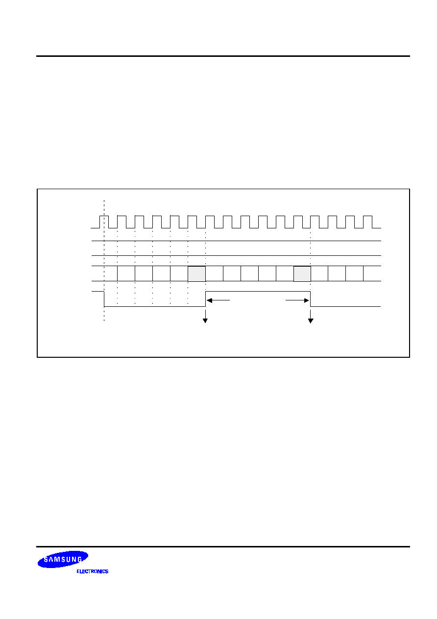
KS57C0502/C0504/P0504 MICROCONTROLLER
TIMERS and TIMER/COUNTER
1117
TC0 COUNTER REGISTER (TCNT0)
The 8-bit counter register for timer/counter, TCNT0, is mapped to RAM addresses F94HF95H. It is read-only
and can be addressed by 8-bit RAM control instructions.
RESET
sets all TCNT0 register values to logic zero
(00H).
Whenever TMOD0.3 are enabled, TCNT0 is cleared to logic zero and counting begins. The TCNT0 register
value is incremented each time an incoming clock signal is detected that matches the signal edge and frequency
setting of the TMOD0 register (specifically, TMOD0.6, TMOD0.5, and TMOD0.4).
Each time TCNT0 is incremented, the new value is compared to the reference value stored in the TC0 refer-
ence register, TREF0. When TCNT0 = TREF0, an overflow occurs in the TCNT0 register, the interrupt request
flag, IRQT0, is set to logic one, and an interrupt request is generated to indicate that the specified timer/counter
interval has elapsed.
COUNTING
STARTS
COUNT
CLOCK
TCNT0
TOL0
TREF0
REFERENCE VALUE = n
0
1
2
. . . n-1
n
0
1
2
. . . n-1
0
1
2
n
n
. . .
IRQT0
SET
IRQT0
SET
INTERVAL TIME
Figure 113. TC0 Timing Diagram
TIMERS and TIMER/COUNTER
KS57C0502/C0504/P0504 MICROCONTROLLER
1118
TC0 REFERENCE REGISTER (TREF0)
The TC0 reference register TREF0 is an 8-bit write-only register that is mapped to RAM locations F96H and
F97H. It is addressable by 8-bit RAM control instructions.
RESET
initializes the TREF0 value to 'FFH'.
TREF0 is used to store a reference value to be compared to the incrementing TCNT0 register in order to iden-
tify an elapsed time interval. Reference values will differ depending upon the specific function that TC0 is being
used to perform -- as a programmable timer/counter, event counter, clock signal divider, or arbitrary frequency
output source.
During timer/counter operation, the value loaded into the reference register compared to the TCNT0 value.
When TCNT0 = TREF0, the TC0 output latch (TOL0) is inverted and an interrupt request is generated to signal
the interval or event.
The TREF0 value, together with the TMOD0 clock frequency selection, determines the specific TC0 timer in-
terval. Use the following formula to calculate the correct value to load to the TREF0 reference register:
TC0 timer interval = (TREF0 value + 1)
×
1
TMOD0 frequency setting
( assuming a TREF0 value
0 )
TC0 OUTPUT ENABLE FLAG (TOE0)
The 1-bit timer/counter 0 output enable flag TOE0 controls output from timer/counter 0 to the TCLO0 pin.
TOE0 is mapped to RAM location F92H.2 and is addressable by 1-bit read and write instructions.
Bit 3
Bit 2
Bit 1
Bit 0
F92H
0
TOE0
0
0
When you set the TOE0 flag to "1", the contents of TOL0 can be output to the TCLO0 pin. Whenever a
RESET
occurs, TOE0 is automatically set to logic zero, disabling all TC0 output. Even when the TOE0 flag is disabled,
timer/counter can continue to output an internally-generated clock frequency, via TOL0, to the serial I/O clock
selector circuit.
TC0 OUTPUT LATCH (TOL0)
TOL0 is the output latch for timer/counter. When the 8-bit comparator detects a correspondence between the
value of the counter register TCNT0 and the reference value stored in the TREF0 buffer, the TOL0 value is
inverted -- the latch toggles high-to-low or low-to-high.
Whenever the state of TOL0 is switched, the TC0 signal is output. TC0 output may be directed to the TCLO0
pin at P3.1, or it can be output directly to the serial I/O clock selector circuit as the
SCK
signal.
Assuming TC0 is enabled, when bit 3 of the TMOD0 register is set to "1", the TOL0 latch is cleared to logic
zero, along with the counter register TCNT0 and the interrupt request flag, IRQT0, and counting resumes
immediately. When TC0 is disabled (TMOD0.2 = "0"), the contents of the TOL0 latch are retained and can be
read, if necessary.

KS57C0502/C0504/P0504 MICROCONTROLLER
TIMERS and TIMER/COUNTER
1119
+
+
PROGRAMMING TIP -- Setting a TC0 Timer Interval
To set a 30 ms timer interval for TC0, given fx = 4.19 MHz, follow these steps.
1.
Select the timer/counter mode register with a maximum setup time of 62.5 ms (assume the TC0 counter
clock = fx/2
10
, and TREF0 is set to FFH):
2.
Calculate the TREF0 value:
30 ms =
TREF0 value + 1
4.09 kHz
TREF0 + 1 =
30 ms
244 µs
= 122.9 = 7AH
TREF0 value = 7AH 1 = 79H
3.
Load the value 79H to the TREF0 register:
BITS
EMB
SMB
15
LD
EA,#79H
LD
TREF0,EA
LD
EA,#4CH
LD
TMOD0,EA

TIMERS and TIMER/COUNTER
KS57C0502/C0504/P0504 MICROCONTROLLER
1120
WATCH TIMER
OVERVIEW
The watch timer is a multi-purpose timer consisting of three basic components:
-- 8-bit watch timer mode register (WMOD)
-- Clock selector
-- Frequency divider circuit
Watch timer functions include real-time and watch-time measurement and interval timing for the system clock.
It is also used as a clock source for generating buzzer output.
Real-Time and Watch-Time Measurement
To start watch timer operation, set bit 2 of the watch timer mode register, WMOD.2, to logic one. The watch
timer starts, the interrupt request flag IRQW is automatically set to logic one, and interrupt requests commence in
0.5-second intervals.
Since the watch timer functions as a quasi-interrupt instead of a vectored interrupt, the IRQW flag should be
cleared to logic zero by program software as soon as a requested interrupt service routine has been executed.
Using a System Clock Source
The watch timer can generate interrupts based on the system clock frequency. The system clock (fx) is used
as the signal source, according to the following formula:
Watch timer clock (fw) =
System clock (fx)
128
= 32.768 kHz
(assuming fx = 4.19 MHz)
Buzzer Output Frequency Generator
The watch timer can generate a steady 2 kHz, 4 kHz, 8 kHz, or 16 kHz signal to the BUZ pin. To select the
BUZ frequency you want, load the appropriate value to the WMOD register. This output can then be used to
actuate an external buzzer sound. To generate a BUZ signal, three conditions must be met:
-- The WMOD.7 register bit at F89H.3 is set to "1"
-- The output latch for I/O port 6.3 is cleared to "0"
-- The port 6.3 output mode flag (PM6.3) set to 'output' mode
Timing Tests in High-Speed Mode
By setting WMOD.1 (F88H.1) to "1", the watch timer will function in high-speed mode, generating an interrupt
every 3.91 ms. At its normal speed (WMOD.1 = '0'), the watch timer generates an interrupt request every 0.5
seconds. High-speed mode is useful for timing events for program debugging sequences.
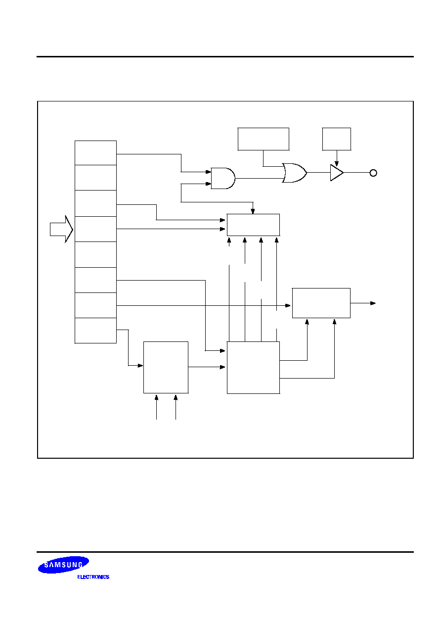
KS57C0502/C0504/P0504 MICROCONTROLLER
TIMERS and TIMER/COUNTER
1121
WATCH TIMER CIRCUIT
fx = SYSTEM CLOCK
fw = WATCH TIMER FREQUENCY
8
IRQW
GND fx/128
fw
32.768 kHz
fw/16
(2 KHz)
BUZ
fw/8
(4 kHz)
fw/2
7
fw/2 (2 Hz)
14
ENABLE /
DISABLE
fw/4
(8 kHz)
fw/2
(16 kHz)
WMOD.7
0
WMOD.5
WMOD.4
0
WMOD.2
WMOD.1
0
SELECTOR
CIRCUIT
CLOCK
SELECTOR
MUX
FREQUENCY
DIVIDING
CIRCUIT
P6.3 LATCH
PM6.3
Figure 114. Watch Timer Circuit Diagram
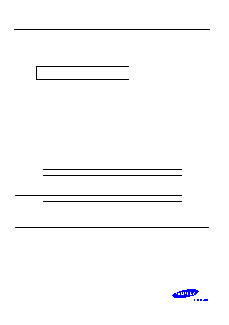
TIMERS and TIMER/COUNTER
KS57C0502/C0504/P0504 MICROCONTROLLER
1122
WATCH TIMER MODE REGISTER (WMOD)
The watch timer mode register WMOD is used to select specific watch timer operations. It is mapped to RAM
locations F88HF89H and is 8-bit write-only addressable.
RESET
sets all WMOD bits to logic zero.
F88H
"0"
WMOD.2
WMOD.1
"0"
F89H
WMOD.7
"0"
WMOD.5
WMOD.4
In brief, WMOD settings control the following watch timer functions:
-- Watch timer speed control
(WMOD.1)
-- Enable/disable watch timer
(WMOD.2)
-- Buzzer frequency selection
(WMOD.4)
(WMOD.5)
-- Enable/disable buzzer output
(WMOD.7)
Table 118. Watch Timer Mode Register (WMOD) Organization
Bit Name
Values
Function
Address
WMOD.7
0
Disable buzzer (BUZ) signal output
1
Enable buzzer (BUZ) signal output
WMOD.6
"0"
Always logic zero
WMOD.5 .4
0
0
2 kHz buzzer (BUZ) signal output
F89H
0
1
4 kHz buzzer (BUZ) signal output
1
0
8 kHz buzzer (BUZ) signal output
1
1
16 kHz buzzer (BUZ) signal output
WMOD.3
"0"
Always logic zero
WMOD.2
0
Disable watch timer; clear frequency dividing circuits
1
Enable watch timer
F88H
WMOD.1
0
Normal mode; sets IRQW to 0.5 seconds
1
High-speed mode; sets IRQW to 3.91 ms
WMOD.0
0
Always logic zero
NOTE
:
System clock frequency (fx) is assumed to be 4.19 MHz.

KS57C0502/C0504/P0504 MICROCONTROLLER
TIMERS and TIMER/COUNTER
1123
+
+
PROGRAMMING TIP -- Using the Watch Timer
1.
Select a 0.5 second interrupt, and 2 kHz buzzer enable:
BITS
EMB
SMB
15
LD
EA,#80H
LD
PMG3,EA
;
P6.3
Output mode
BITR
P6.3
;
Clear P6.3 output latch
LD
EA,#84H
LD
WMOD,EA
BITS
IEW
2.
Sample real-time clock processing method:
CLOCK
BTSTZ
IRQW
;
0.5 second check
RET
;
No, return
·
;
Yes, 0.5 second interrupt generation
·
·
;
Increment HOUR, MINUTE, SECOND

TIMERS and TIMER/COUNTER
KS57C0502/C0504/P0504 MICROCONTROLLER
1124
NOTES

KS57C0502/C0504/P0504 MICROCONTROLLER
COMPARATOR
121
12
COMPARATOR
OVERVIEW
Port 2 can be used as a analog input port for a comparator. The reference voltage for the 4-channel
comparator can be supplied either internally or externally at P2.3. When internal reference voltage is used, four
channels (P2.0P2.3) are used for analog inputs and the internal reference voltage is varies at 16 levels. If an
external reference voltage is input at P2.3, the other three pins (P2.0P2.2) in port 2 are used for analog input.
Unused port 2 pins must be connected to V
DD
.
When a conversion is completed, the result is saved in the comparison result register CMPREG. The initial
values of the CMPREG are undefined and the comparator operation is disabled by a
RESET
. The comparator has
following components:
-- Comparator
-- Internal reference voltage generator (4-bit resolution)
-- External reference voltage source at P2.3
-- Comparator mode register (CMOD)
-- Comparison result register (CMPREG)
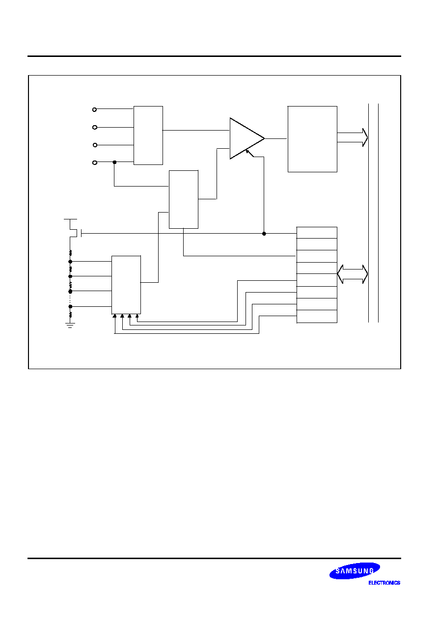
COMPARATOR
KS57C0502/C0504/P0504 MICROCONTROLLER
122
P2.0 / CIN0
P2.1 / CIN1
P2.2 / CIN2
P2.3 / CIN3
COMPARISON
RESULT
REGISTER
(CMPREG)
8
M
U
X
V
DD
1/2R
R
R
1/2R
CMOD.7
CMOD.6
CMOD.5
0
CMOD.3
CMOD.2
CMOD.1
CMOD.0
V
REF
(INTERNAL)
+
INTERNAL BUS
M
U
X
4
M
U
X
V
REF
(EXTERNAL)
Figure 121. Comparator Circuit Diagram
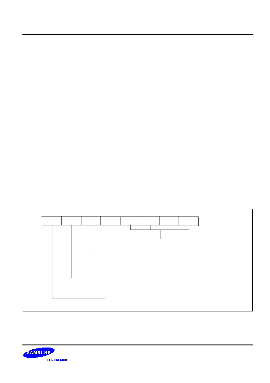
KS57C0502/C0504/P0504 MICROCONTROLLER
COMPARATOR
123
COMPARATOR MODE REGISTER (CMOD)
The comparator mode register CMOD is an 8-bit register that is used to set the operation mode of the
comparator. It is mapped to addresses FD6HFD7H and can be manipulated using 8-bit memory instructions.
Based on the CMOD.5 bit setting, an internal or an external reference voltage is input for the comparator, as
follows:
When CMOD.5 is set to logic zero:
-- A reference voltage is selected by the CMOD.0 to CMOD.3 bit settings.
-- P2.0 to P2.3 are used as analog input pins.
-- The internal digital to analog converter generates 16 reference voltages.
-- The comparator can detect 150 mV difference between the reference voltage and the analog input
voltages.
-- Comparator results are written into 4-bit comparison result register (CMPREG).
When CMOD.5 is set to logic one:
-- An external reference voltage is supplied from P2.3/CIN3.
-- P2.0 to P2.2 are used as the analog input pins.
-- The comparator can detect 150 mV difference between the reference voltage and the analog input
voltages.
-- Bits 02 in the CMPREG register contain the results; the content of bit 3 is not used.
Bit 6 in the CMOD register controls conversion time while bit 7 enables or disables comparator operation to
reduce power consumption. A
RESET
signal clears all bits to logic zero, causing the comparator operation to
enter stop mode.
CMOD.7 CMOD.6 CMOD.5
0
CMOD.3 CMOD.2 CMOD.1 CMOD.0
1: CIN3; external reference, CIN02; analog input
0: Internal reference, CIN03; analog input
Reference voltage (V
REF
) selection:
VDD x (n + 0.5)/16, n = 0 to 15
1: Conversion time (4 x 2 /fx, 15.2 µs @4.19MHz)
0: Conversion time (4 x 2 /fx, 121.6 µs @4.19MHz)
1: Comparator operation enable
0: Comparator operation disable
4
7
FD6HFD7H
Figure 122. Comparator Mode Register Organization
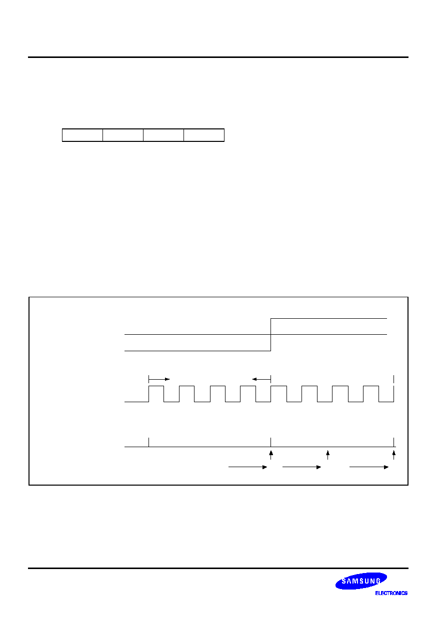
COMPARATOR
KS57C0502/C0504/P0504 MICROCONTROLLER
124
PORT 2 MODE REGISTER (P2MOD)
P2MOD register settings determine if port 2 is used for analog or digital input. The P2MOD register is 4-bit
write only register. P2MOD is mapped to address FE2H and initialized to logic zero by a
RESET
, which configures
port 2 as an analog input port.
FE2H
P2MOD.3
P2MOD.2
P2MOD.1
P2MOD.0
When bit is set to "1", the corresponding pin is configured as a digital input pin. When set to "0", configured as
an analog input pin: P2MOD.0 for P2.0, P2MOD.1 for P2.1, P2MOD.2 for P2.2, and P2MOD.3 for P2.3.
COMPARATOR OPERATION
The comparator compars analog voltage input at CIN0CIN3 with an external or internal reference voltage
(V
REF
) that is selected by CMOD register. The result is written to the comparison result register CMPREG at
address FD4H. The comparison result is calculated as follows.
If "1" Analog input voltage
V
REF
+ 150 mV
If "0" Analog input voltage
V
REF
150 mV
To obtain a comparison result, the data must be read out from the CMPREG register after V
REF
is updated by
changing the CMOD value after a conversion time has elapsed.
ANALOG INPUT
VOLTAGE (CIN03)
REFERENCE
VOLTAGE (V
REF
)
COMPARATOR CLOCK
(CMPCLK, fx/16, fx/128)
COMPARISON
RESULT (CMPREG)
COMPARISON TIME
(CMPCLK x 4)
COMPARISON
END
1
0
COMPARISON
START
UNKNOWN
1
Figure 123. Conversion Characteristics

KS57C0502/C0504/P0504 MICROCONTROLLER
COMPARATOR
125
+
+
PROGRAMMING TIP -- Programming the Comparator
The following code converts the analog voltage input at CIN0CIN2 pins into 4-bit digital code.
BITR
EMB
LD
A,#0H
LD
P2MOD,A
;
Analog input selection (CIN0CIN3)
LD
EA,#8XH
;
x = 0F, comparator enable
;
Internal reference, conversion time (121.6 µs)
LD
CMOD,EA
WAIT
LD
A,#0H
INCS
A
JR
WAIT
LD
A,CMPREG
;
Read the result
LD
P4,A
;
Output the result from port 4

COMPARATOR
KS57C0502/C0504/P0504 MICROCONTROLLER
126
NOTES

KS57C0502/C0504/P0504 MICROCONTROLLER
SERIAL I/O INTERFACE
131
13
SERIAL I/O INTERFACE
OVERVIEW
The serial I/O interface (SIO) has the following functional components:
-- 8-bit mode register (SMOD)
-- Clock selector circuit
-- 8-bit buffer register (SBUF)
-- 3-bit serial clock counter
Using the serial I/O interface, you can exchange 8-bit data with an external device. You control the
transmission frequency by the appropriate bit settings to the SMOD register.
The serial interface can run off an internal or an external clock source, or the TOL0 signal that is generated by
the 8-bit timer/counter 0, TC0. If you use the TOL0 clock signal, you can modify its frequency to adjust the serial
data transmission rate.
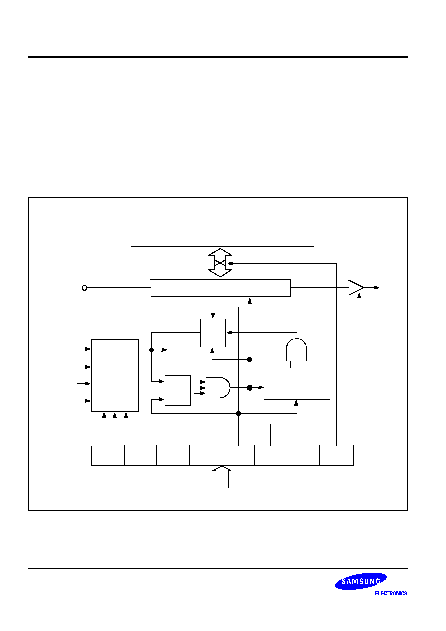
SERIAL I/O INTERFACE
KS57C0502/C0504/P0504 MICROCONTROLLER
132
SIO OPERATION SEQUENCE
The general sequence of operations for the serial I/O interface may be summarized as follows:
1.
Set SIO mode to transmit-and-receive or to receive-only.
2.
Select MSB-first or LSB-first transmission mode.
3.
Set the
SCK
clock signal in the mode register, SMOD.
4.
Set SIO interrupt enable flag (IES) to "1".
5.
Initiate SIO transmission by setting bit 3 of the SMOD to "1".
6.
When the SIO operation is complete, IRQS flag is set and an interrupt is generated.
INTERNAL BUS
LSB or MSB first
SI
IRQS
CLK
CLK
CLK
CLEAR
SCK
TOL0
fx/2
10
fx/2
SO
8
8
SBUF (8-BIT)
CLOCK
SELECTOR
R
Q
D
Q0
Q1
Q2
3-BIT COUNTER
R
S
Q
SMOD.7 SMOD.6 SMOD.5
SMOD.3 SMOD.2 SMOD.1
SMOD.0
Figure 131. Serial I/O Interface Circuit Diagram
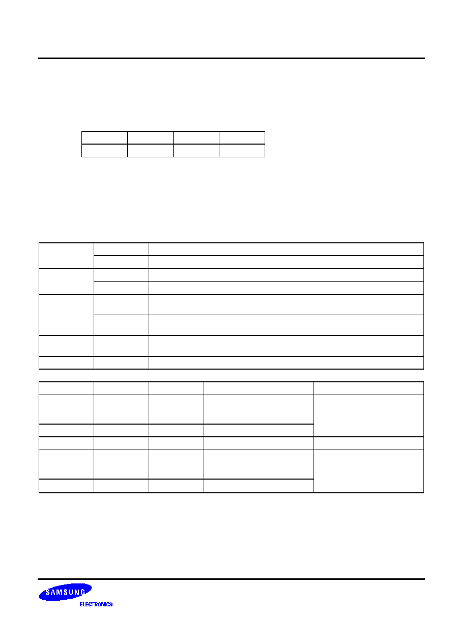
KS57C0502/C0504/P0504 MICROCONTROLLER
SERIAL I/O INTERFACE
133
SERIAL I/O MODE REGISTER (SMOD)
The serial I/O mode register, SMOD, is an 8-bit register that specifies the operation mode of the serial
interface. SMOD is mapped to RAM address FE0HFE1H and its reset value is logic zero. SMOD is organized in
two 4-bit registers, as follows:
FE0H
SMOD.3
SMOD.2
SMOD.1
SMOD.0
FE1H
SMOD.7
SMOD.6
SMOD.5
0
SMOD register settings enable you to select either MSB-first or LSB-first serial transmission, and to operate in
transmit-and-receive mode or receive-only mode.
SMOD is a write-only register and can be addressed only by 8-bit RAM control instructions. One exception to
this is SMOD.3, which can be written by a 1-bit RAM control instruction. When SMOD.3 is set to 1, the contents
of the serial interface interrupt request flag, IRQS, and the 3-bit serial clock counter are cleared, and SIO
operations are initiated. When the SIO transmission starts, SMOD.3 is cleared to logic zero.
Table 131. SIO Mode Register (SMOD) Organization
SMOD.0
0
Most significant bit (MSB) is transmitted first
1
Least significant bit (LSB) is transmitted first
SMOD.1
0
Receive-only mode; output buffer is off
1
Transmit-and-receive mode
SMOD.2
0
Disable the data shifter and clock counter; retain contents of IRQS flag when
serial transmission is halted
1
Enable the data shifter and clock counter; set IRQS flag to "1" when serial
transmission is halted
SMOD.3
1
Clear IRQS flag and 3-bit clock counter to "0"; initiate transmission and then
reset this bit to logic zero
SMOD.4
0
Bit not used; value is always "0"
SMOD.7
SMOD.6
SMOD.5
Clock Selection
R/W Status of SBUF
0
0
0
External clock at
SCK
pin
SBUF is enabled when SIO
operation is halted or when
SCK
goes high.
0
0
1
Use TOL0 clock from TC0
0
1
x
CPU clock: fx/4, fx/8, fx/64
Enable SBUF read/write
1
0
0
4.09 kHz clock: fx/2
10
SBUF is enabled when SIO
operation is halted or when
SCK
goes high.
1
1
1
262 kHz clock: fx/2
4
NOTES:
1.
'fx' = system clock; 'x' means 'don't care.'
2.
kHz frequency ratings assume a system clock (fx) running at 4.19 MHz.
3.
The SIO clock selector circuit cannot select a fx/2
4
clock if the CPU clock is fx/64
.
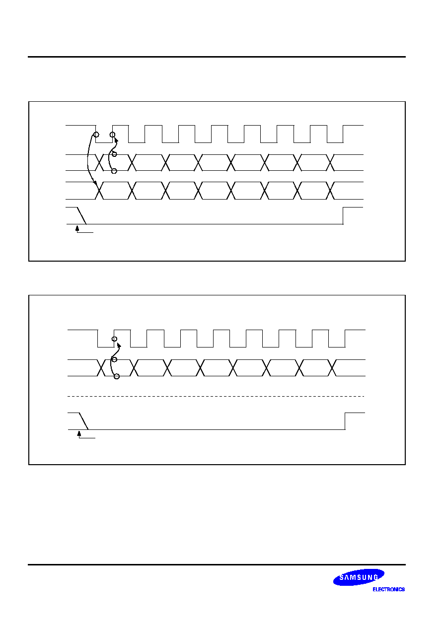
SERIAL I/O INTERFACE
KS57C0502/C0504/P0504 MICROCONTROLLER
134
SERIAL I/O TIMING DIAGRAMS
SCK
SI
SO
IRQS
DI7
DI6
DI5
DI4
DI3
DI2
DI1
DI0
DO7
DO6
DO5
DO4
DO3
DO2
DO1
DO0
TRANSMIT
COMPLETE
SET SMOD.3
Figure 132. SIO Timing in Transmit/Receive Mode
HIGH IMPEDANCE
SCK
SI
IRQS
TRANSMIT
COMPLETE
SET SMOD.3
DI7
DI6
DI5
DI4
DI3
DI2
DI1
DI0
SO
Figure 133. SIO Timing in Receive-Only Mode
KS57C0502/C0504/P0504 MICROCONTROLLER
SERIAL I/O INTERFACE
135
SERIAL I/O BUFFER REGISTER (SBUF)
When the serial interface operates in transmit-and-receive mode (SMOD.1 = "1"), transmit data in the SIO
buffer register are output to the SO pin (P0.1) at the rate of one bit for each falling edge of the SIO clock.
Receive data is simultaneously input from the SI pin (P0.2) to SBUF at the rate of one bit for each rising edge of
the SIO clock.
When receive-only mode is used, incoming data is input to the SIO buffer at the rate of one bit for each rising
edge of the SIO clock.
SBUF can be read or written using 8-bit RAM control instructions. It is mapped to addresses FE4HFE5H.
Following a
RESET
, the value of SBUF is undetermined.
+
+
PROGRAMMING TIP -- Setting Transmit/Receive Modes for Serial I/O
1.
Transmit the data value 48H through the serial I/O interface using an internal clock frequency of fx/2
4
and
in MSB-first mode:
BITS
EMB
SMB
15
LD
EA,#03H
LD
PMG1,EA
;
P0.0 /
SCK
and P0.1 / SO
Output
LD
EA,#48H
;
LD
SBUF,EA
;
LD
EA,#0EEH
LD
SMOD,EA
;
SIO data transfer
EXTERNAL
DEVICE
SCK
/ P0.0
SO / P0.1
2.
Use CPU clock to transfer and receive serial data at high speed:
BITS
EMB
SMB
15
LD
EA,#03H
LD
PMG1,EA
;
P0.0 /
SCK
and P0.1 / SO
Output, P0.2 / SI
Input
LD
EA,TDATA
LD
SBUF,EA
LD
EA,#4FH
LD
SMOD,EA
;
SIO start
BITR
IES
STEST
BTSTZ
IRQS
JR
STEST
LD
EA,SBUF
SMB
0
LD
RDATA,EA
SERIAL I/O INTERFACE
KS57C0502/C0504/P0504 MICROCONTROLLER
136
+
+
PROGRAMMING TIP -- Setting Transmit/Receive Modes for Serial I/O (Continued)
3.
Transmit and receive an internal clock frequency of 4.09 kHz (at 4.19 MHz) in LSB-first mode:
BITS
EMB
SMB
15
LD
EA,#03H
LD
PMG1,EA
;
P0.0 /
SCK
and P0.1 / SO
Output, P0.2/SI
Input
LD
EA,TDATA
LD
SBUF,EA
LD
EA,#8FH
LD
SMOD,EA
;
SIO start
EI
BITS
IES
·
·
INTS
PUSH
SB
;
Store SMB, SRB
PUSH
EA
;
Store EA
LD
EA,TDATA
;
EA
Transmit data
SMB
15
XCH
EA,SBUF
;
EA
Receive data
SMB
0
LD
RDATA,EA
;
RDATA
Receive data
BITS
SMOD.3
;
SIO start
POP
EA
POP
SB
IRET
EXTERNAL
DEVICE
SCK
/ P0.0
SO / P0.1
SI / P0.2
KS57C0502/C0504/P0504 MICROCONTROLLER
SERIAL I/O INTERFACE
137
+
+
PROGRAMMING TIP -- Setting Transmit/Receive Modes for Serial I/O (Continued)
4.
Transmit and receive an external clock in LSB-first mode:
BITS
EMB
SMB
15
LD
EA,#02H
LD
PMG1,EA
;
P0.1 / SO
Output, P0.0 /
SCK
and P0.2 / SI
Input
LD
EA,TDATA
LD
SBUF,EA
LD
EA,#0FH
LD
SMOD,EA
;
SIO start
EI
BITS
IES
·
·
INTS
PUSH
SB
;
Store SMB, SRB
PUSH
EA
;
Store EA
LD
EA,TDATA
;
EA
Transmit data
SMB
15
XCH
EA,SBUF
;
EA
Receive data
SMB
0
LD
RDATA,EA
;
RDATA
Receive data
BITS
SMOD.3
;
SIO start
POP
EA
POP
SB
IRET
EXTERNAL
DEVICE
SCK
/ P0.0
SO / P0.1
SI / P0.2
High Speed SIO Transmission

SERIAL I/O INTERFACE
KS57C0502/C0504/P0504 MICROCONTROLLER
138
+
+
PROGRAMMING TIP -- Setting Transmit/Receive Modes for Serial I/O (Concluded)
Use CPU clock to transfer and receive serial data at high speed:
BITS
EMB
SMB
15
LD
EA,#03H
LD
PMG1,EA
;
P0.0 / SCK and P0.1 / SO
Output, P0.2 / SI
Input
LD
EA,TDATA
LD
SBUF,EA
LD
EA,#4FH
LD
SMOD,EA
;
SIO start
BITR
IES
STEST
BTSTZ
IRQS
JR
STEST
LD
EA,SBUF
SMB
0
LD
RDATA,EA
KS57C0502/C0504/P0504 MICROCONTROLLER
ELECTRICAL DATA
141
14
ELECTRICAL DATA
Table 141. Absolute Maximum Ratings
(T
A
= 25
°
C)
Parameter
Symbol
Conditions
Rating
Units
Supply Voltage
V
DD
0.3 to + 6.5
V
Input Voltage
V
I
All I/O ports
0.3 to V
DD
+ 0.3
V
Output Voltage
V
O
0.3 to V
DD
+ 0.3
V
Output Current High
I
O H
One I/O port active
5
mA
All I/O ports active
15
Output Current Low
I
O L
Ports 0, 3, and 6
5
mA
Ports 4 and 5
30
All ports, total
+ 100
Operating Temperature
T
A
40 to + 85
°
C
Storage Temperature
T
stg
65 to + 150
°
C
Table 142. D.C. Electrical Characteristics
(T
A
= 40
°
C to + 85
°
C, V
DD
= 1.8 V to 5.5 V)
Parameter
Symbol
Conditions
Min
Typ
Max
Units
Input High
Voltage
V
IH1
Ports 4 and 5
0.7V
DD
V
DD
V
V
IH2
Ports 0, 1, 2, 3, 6, and
RESET
0.8V
DD
V
DD
V
IH3
X
in
and X
out
V
DD
0.1
V
DD
Input Low
Voltage
V
IL1
Ports 4 and 5
0.3V
DD
V
V
IL2
Ports 0, 1, 2, 3, 6,
and RESET
0.2V
DD
V
IL3
X
in
and X
out
0.1
Output High
Voltage
V
OH
V
DD
= 4.5 V to 5.5 V
I
OH
= 1 mA
Ports 0, 3, 4, 5, 6
V
DD
- 1.0
V
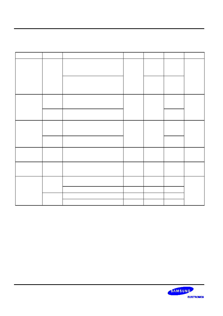
ELECTRICAL DATA
KS57C0502/C0504/P0504 MICROCONTROLLER
142
Table 142. D.C. Electrical Characteristics (Continued)
(T
A
= 40
°
C to + 85
°
C, V
DD
= 1.8 V to 5.5 V)
Parameter
Symbol
Conditions
Min
Typ
Max
Units
Output Low
Voltage
V
OL
V
DD
= 4.5 V to 5.5 V
I
OL
= 15 mA
Ports 4, 5
2
V
VDD = 4.5V to 5.5 V
I
OL
= 4.0mA
All output pins except Ports 4, 5
2
Input High
Leakage
Current
I
LIH1
V
IN
= V
DD
All input pins except X
in
and X
out
3
µ
A
I
LIH2
V
IN
= V
DD
X
in
and X
out
20
Input Low
Leakage
Current
I
LIL1
V
IN
= 0 V
All input pins except X
in,
X
out
and
RESET
3
µ
A
I
LIL2
V
IN
= 0 V
X
in
and X
out
20
Output High
Leakage
Current
I
LOH
V
O
= V
DD
All output pins
3
µ
A
Output Low
Leakage
Current
I
LOL
V
O
= 0 V
3
µ
A
Pull-Up
Resistor
R
L1
V
I
= 0 V; V
DD
= 5 V
Port 0, 1, 3, 4, 5, 6
25
50
100
k
V
DD
= 3 V
50
100
200
R
L2
V
DD
= 5 V; V
I
= 0 V;
RESET
100
250
400
V
DD
= 3 V
200
500
800
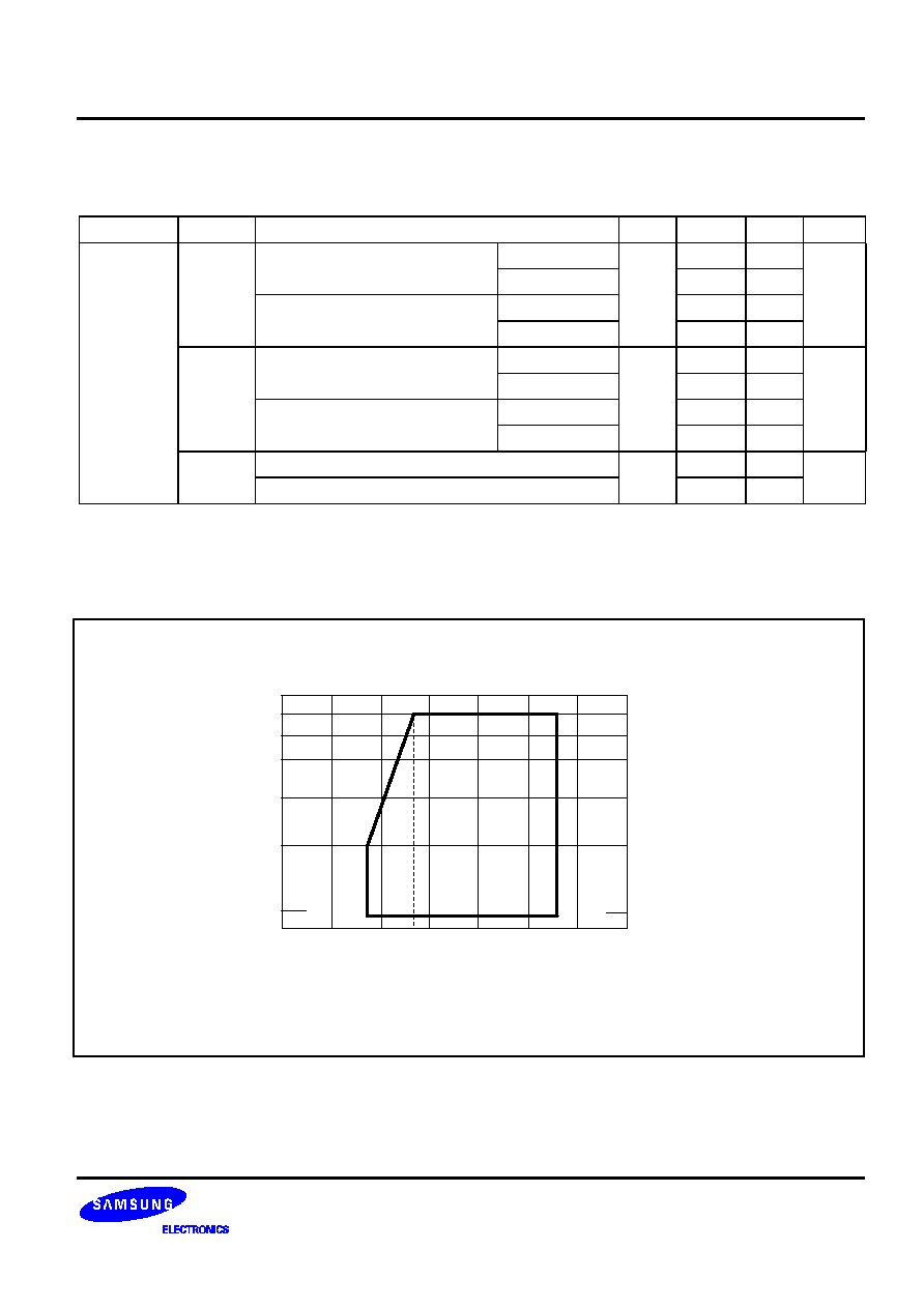
KS57C0502/C0504/P0504 MICROCONTROLLER
ELECTRICAL DATA
143
Table 142. D.C. Electrical Characteristics (Concluded)
(T
A
= 40
°
C to + 85
°
C, V
DD
= 1.8 V to 5.5 V)
Parameter
Symbol
Conditions
Min
Typ
Max
Units
Supply
I
DD1
Run mode; V
DD
= 5.0 V
±
10%
6.0MHz
3.0
8.0
mA
Current
(1)
Crystal oscillator; C1=C2=22pF
4.19MHz
2.0
5.5
V
DD
= 3 V
±
10%
6.0MHz
1.3
4.0
4.19MHz
1.0
3.0
I
DD2
Idle mode; V
DD
= 5.0 V
±
10%
6.0MHz
0.8
2.5
mA
Crystal oscillator; C1=C2=22pF
4.19MHz
0.6
1.8
V
DD
= 3 V
±
10%
6.0MHz
0.6
1.5
4.19MHz
0.4
1.0
I
DD3
Stop mode; V
DD
= 5.0 V
±
10%
0.5
3.0
µ
A
Stop mode; V
DD
= 3.0 V
±
10%
0.3
2.0
NOTES:
1.
D.C. electrical values for Supply current (IDD1 to IDD3) do not include current drawn through internal pull-up registers,
output port drive currents and comparator.
2.
The supply current assumes a CPU clock of fx/4.
CPU CLOCK = 1/n x oscillator frequency (n = 4, 8 or 64)
SUPPLY VOLTAGE (V)
1.05 MHz
15.625 kHz
CPU CLOCK
4.2 MHz
6 MHz
400 kHz
Main Osc. Freq. ( Divided by 4 )
1.5 MHz
1
2
2.7
3
4
5
6
7
Figure 141. Standard Operating Voltage Range
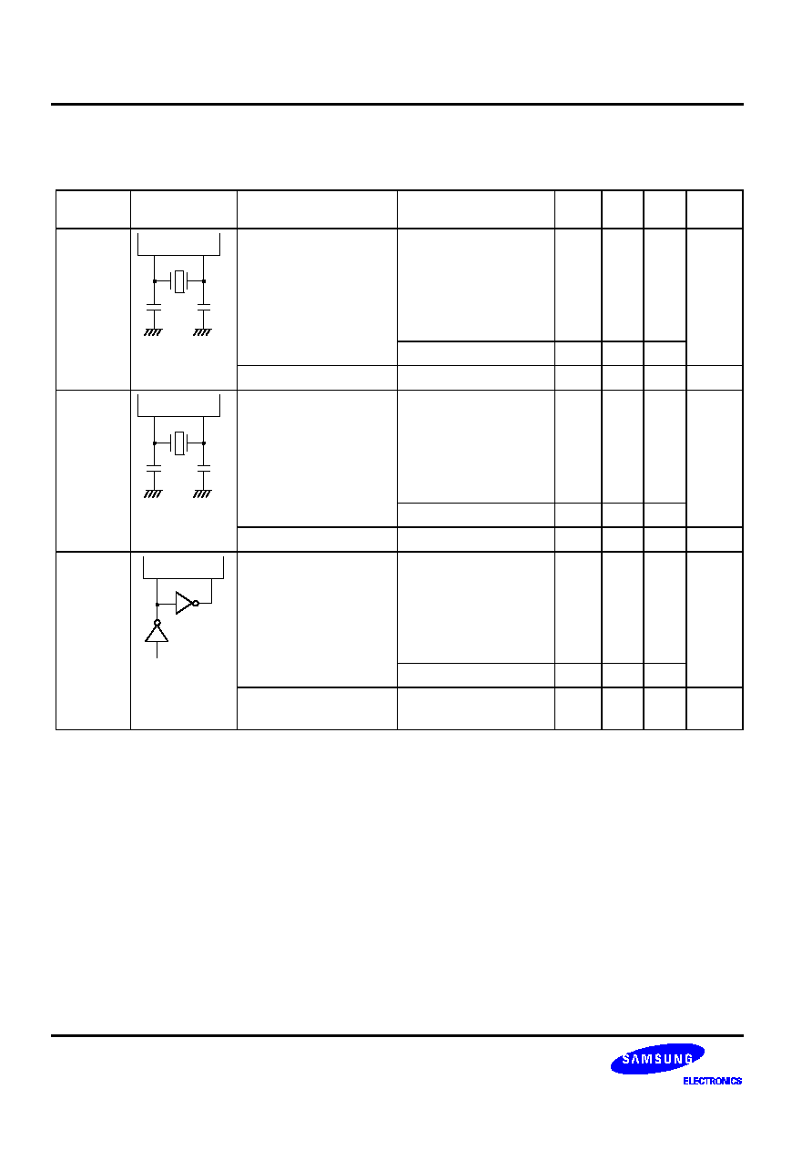
ELECTRICAL DATA
KS57C0502/C0504/P0504 MICROCONTROLLER
144
Table 143. Oscillators Characteristics
(T
A
= 40
°
C + 85
°
C, V
DD
= 1.8 V to 5.5 V)
Oscillator
Clock
Configuration
Parameter
Test Condition
Min
Typ
Max
Units
Ceramic
Oscillator
Xin
Xout
C1
C2
Oscillation frequency
(1)
V
DD
= 2.7 V to 5.5 V
0.4
6.0
MHz
V
DD
= 1.8 V to 5.5 V
0.4
4.2
Stabilization time
(2)
V
DD
= 3.0 V
4
ms
Crystal
Oscillator
Xin
Xout
C1
C2
Oscillation frequency
(1)
V
DD
= 2.7 V to 5.5 V
0.4
6.0
MHz
V
DD
= 1.8 V to 5.5 V
0.4
4.2
Stabilization time
(2)
V
DD
= 3.0 V
10
ms
External
Clock
Xin
Xout
X
in
input frequency
(1)
V
DD
= 2.7 V to 5.5 V
0.4
6.0
MHz
V
DD
= 1.8 V to 5.5 V
0.4
4.2
X
in
input high and low
level width (t
XH
, t
XL
)
83.3
1250
ns
NOTES:
1.
Oscillation frequency and X
in
input frequency data are for oscillator characteristics only.
2.
Stabilization time is the interval required for oscillating stabilization after a power-on occurs, or when stop mode is
terminated.
KS57C0502/C0504/P0504 MICROCONTROLLER
ELECTRICAL DATA
145
Table 144. Input/Output Capacitance
(T
A
= 25
°
C, V
DD
= 0 V )
Parameter
Symbol
Condition
Min
Typ
Max
Units
Input
Capacitance
C
IN
f = 1 MHz; Unmeasured pins
are returned to V
SS
15
pF
Output
Capacitance
C
OUT
15
pF
I/O Capacitance
C
IO
15
pF
Table 145. Comparator Electrical Characteristics
(T
A
= 40
°
C to + 85
°
C, V
DD
= 4.0 V to 5.5V, V
SS
= 0 V)
Parameter
Symbol
Condition
Min
Typ
Max
Units
Input Voltage Range
0
V
DD
V
Reference Voltage
Range
V
REF
0
V
DD
V
Input Voltage Accuracy
V
CIN
±
150
mV
Input Leakage Current
I
CIN,
I
REF
3
3
µ
A
Table 146. A.C. Electrical Characteristics
(T
A
= 40
°
C to + 85
°
C, V
DD
= 1.8 V to 5.5 V)
Parameter
Symbol
Conditions
Min
Typ
Max
Units
Instruction Cycle
Time
t
CY
V
DD
= 2.7 V to 5.5 V
0.67
64
µ
s
V
DD
= 1.8 V to 5.5 V
0.95
TCL0 Input
Frequency
f
TI
V
DD
= 2.7 V to 5.5 V
0
1.5
MHz
V
DD
= 1.8 V to 5.5 V
1
MHz
TCL0 Input High,
Low Width
t
TIH
,
t
TIL
V
DD
= 2.7 V to 5.5 V
0.48
µ
s
V
DD
= 1.8 V to 5.5 V
1.8
SCK
Cycle Time
t
KCY
V
DD
= 2.7 V to 5.5 V
External
SCK
source
800
ns
Internal
SCK
source
670
V
DD
= 1.8 V to 5.5 V
External
SCK
source
3200
Internal
SCK
source
3800
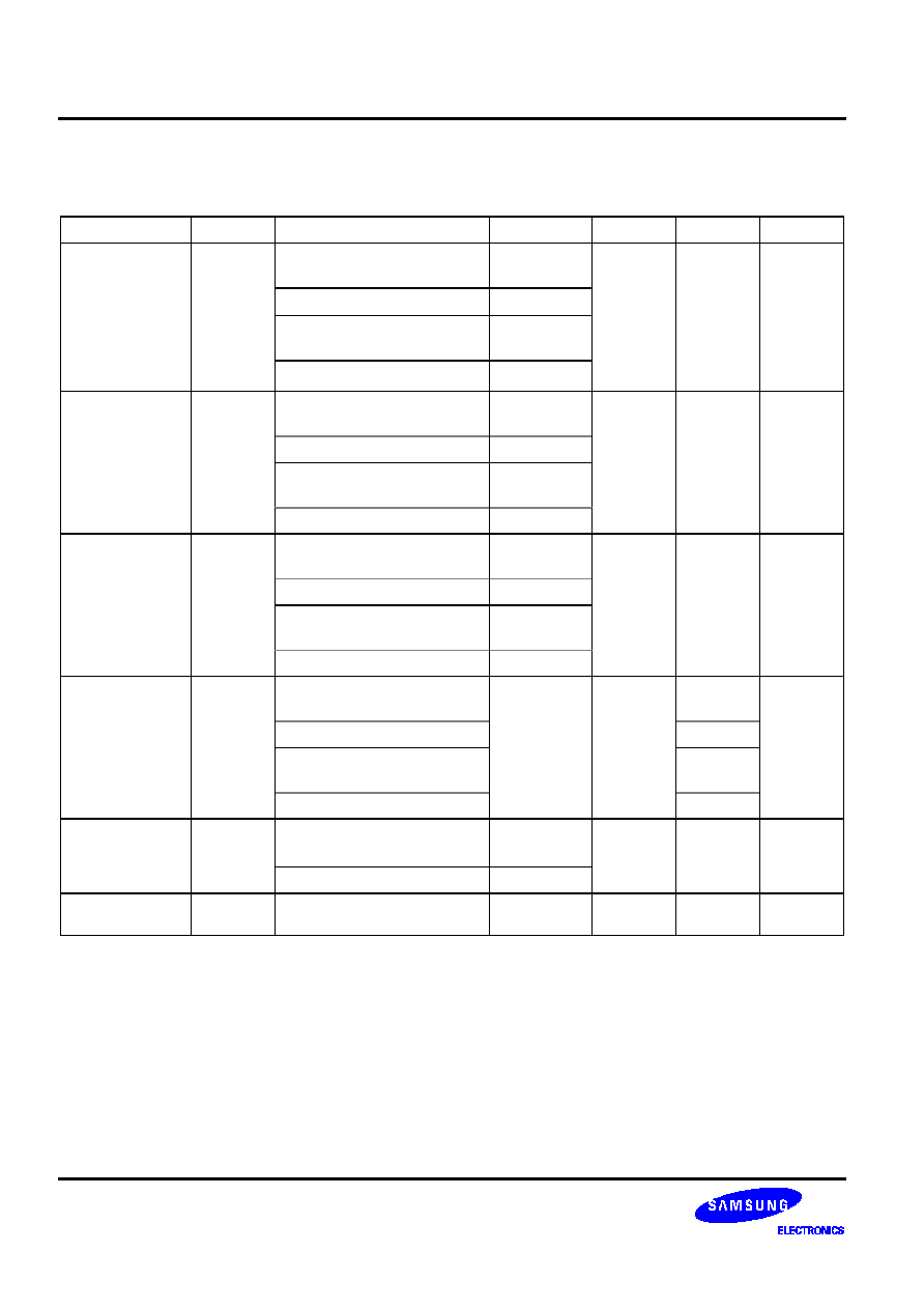
ELECTRICAL DATA
KS57C0502/C0504/P0504 MICROCONTROLLER
146
Table 146. A.C. Electrical Characteristics ( Concluded)
(T
A
= 40
°
C to + 85
°
C, V
DD
= 1.8 V to 5.5 V)
Parameter
Symbol
Conditions
Min
Typ
Max
Units
SCK
High, Low
Width
t
KH
, t
KL
V
DD
= 2.7 V to 5.5 V
External
SCK
source
335
ns
Internal
SCK
source
t
KCY
/2 - 50
V
DD
= 1.8 V to 5.5 V
External
SCK
source
1600
Internal
SCK
source
t
KCY
/
2 - 150
SI Setup Time to
SCK
High
t
SIK
V
DD
= 2.7 V to 5.5 V
External
SCK
source
100
ns
Internal
SCK
source
150
V
DD
= 1.8 V to 5.5 V
External
SCK
source
150
Internal
SCK
source
500
SI Hold Time to
SCK
High
t
KSI
V
DD
= 2.7 V to 5.5 V
External
SCK
source
400
ns
Internal
SCK
source
400
V
DD
= 1.8 V to 5.5 V
External
SCK
source
600
Internal
SCK
source
500
Output Delay for
SCK
to SO
t
KSO
(1)
V
DD
= 2.7 V to 5.5 V
External
SCK
source
300
ns
Internal
SCK
source
250
V
DD
= 1.8 V to 5.5 V
External
SCK
source
1000
Internal
SCK
source
1000
Interrupt Input
High, Low Width
t
INTH
,
t
INTL
INT0
(2)
µ
s
INT1, KS0 - KS2
10
RESET
Input Low
Width
t
RSL
Input
10
µ
s
NOTES:
1.
R(1Kohm) and C (100pF) are the load resistance and load capacitance of the SO output line.
2.
Minimum value for INT0 is based on a clock of 2t
CY
or 128 / fx as assigned by the IMOD0 register setting.
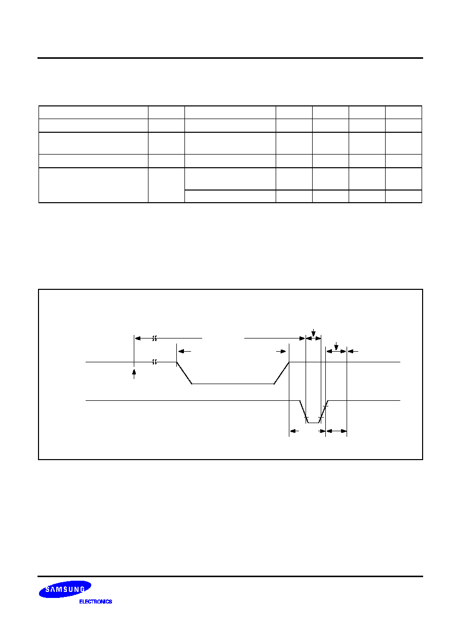
KS57C0502/C0504/P0504 MICROCONTROLLER
ELECTRICAL DATA
147
Table 14-7. RAM Data Retention Supply Voltage in Stop Mode
(T
A
= 40
°
C to + 85
°
C)
Parameter
Symbol
Conditions
Min
Typ
Max
Unit
Data retention supply voltage
V
DDDR
1.8
5.5
V
Data retention supply current
I
DDDR
V
DDDR
= 1.8 V
0.1
10
µ
A
Release signal set time
t
SREL
0
µ
s
Oscillator stabilization wait
time
(1)
t
WAIT
Released by
RESET
2
17
/ fx
ms
Released by interrupt
(2)
ms
NOTES:
1.
During oscillator stabilization wait time, all CPU operations must be stopped to avoid instability during oscillator start-
up.
2.
Use the basic timer mode register (BMOD) interval timer to delay execution of CPU instructions during the wait time.
TIMING WAVEFORMS
t
SREL
t
WAIT
V
DD
RESET
EXECUTION OF
STOP INSTRUCTION
V
DDDR
DATA RETENTION MODE
STOP MODE
INTERNAL RESET
OPERATION
IDLE MODE
OPERATING
MODE
Figure 142. Stop Mode Release Timing When Initiated By
RESET
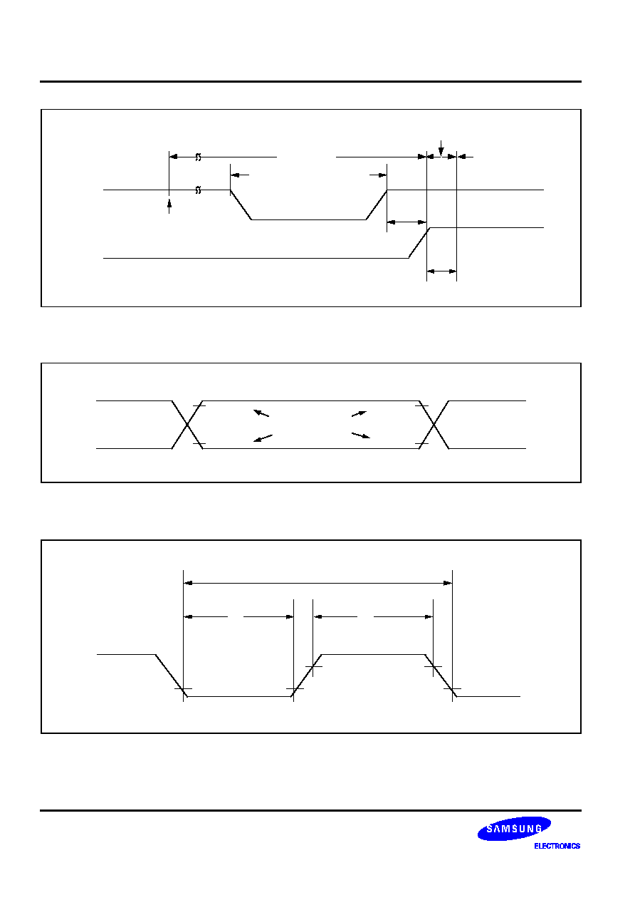
ELECTRICAL DATA
KS57C0502/C0504/P0504 MICROCONTROLLER
148
V
DD
EXECUTION OF
STOP INSTRUCTION
V
DDDR
DATA RETENTION MODE
STOP MODE
t
WAIT
t
SREL
IDLE MODE
NORMAL
OPERATING
MODE
POWER-DOWN MODE TERMINATING SIGNAL
(INTERRUPT REQUEST)
Figure 143. Stop Mode Release Timing When Initiated By Interrupt Request
MEASUREMENT
POINTS
0.8 VDD
0.8 VDD
0.2 VDD
0.2 VDD
Figure 144. A.C. Timing Measurement Points (Except for X
in
)
Xin
t
XL
t
XH
1 / fx
0.2 V
VDD - 0.2 V
Figure 145. Clock Timing Measurement at X
in
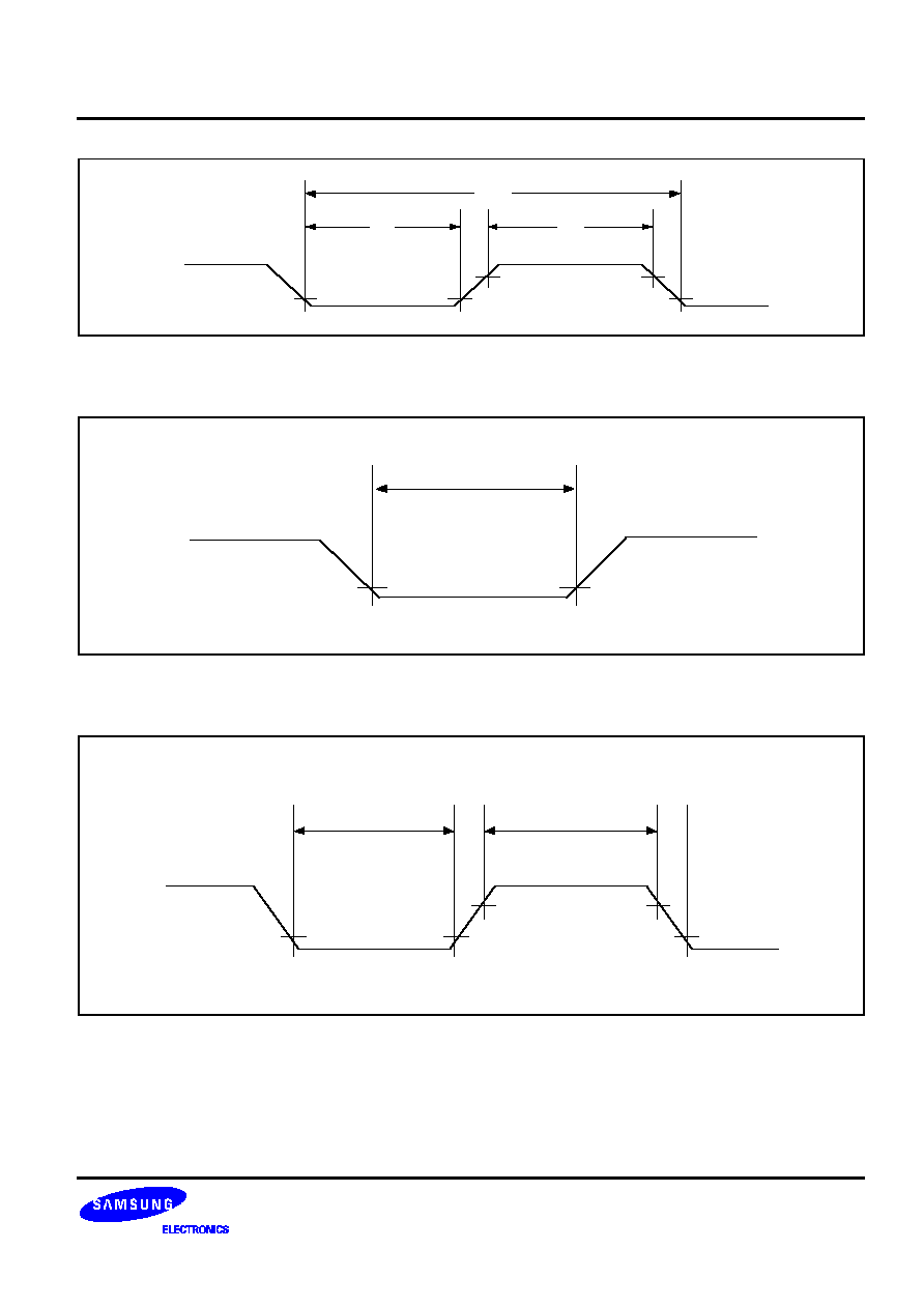
KS57C0502/C0504/P0504 MICROCONTROLLER
ELECTRICAL DATA
149
TCL
t
TIL
t
TIH
1 /
f
TI
0.8 VDD
0.2 VDD
Figure 146. TCL Timing
t
RSL
RESET
0.2
V
DD
Figure 147. Input Timing for
RESET
Signal
INT0, 1
KS0 to KS2
t
INTL
t
INTH
0.2 VDD
0.8 VDD
Figure 148. Input Timing for External Interrupts
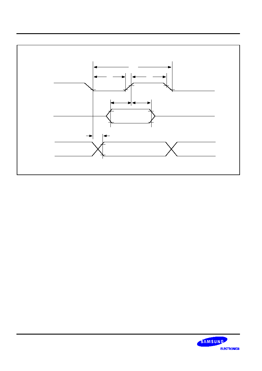
ELECTRICAL DATA
KS57C0502/C0504/P0504 MICROCONTROLLER
1410
SCK
t
KL
t
KH
t
CKY
0.8
V
DD
INPUT DATA
OUTPUT DATA
0.2
V
DD
0.8
V
DD
0.2
V
DD
SI
SO
t
SIK
t
KSI
t
KSO
Figure 149. Serial Data Transfer Timing
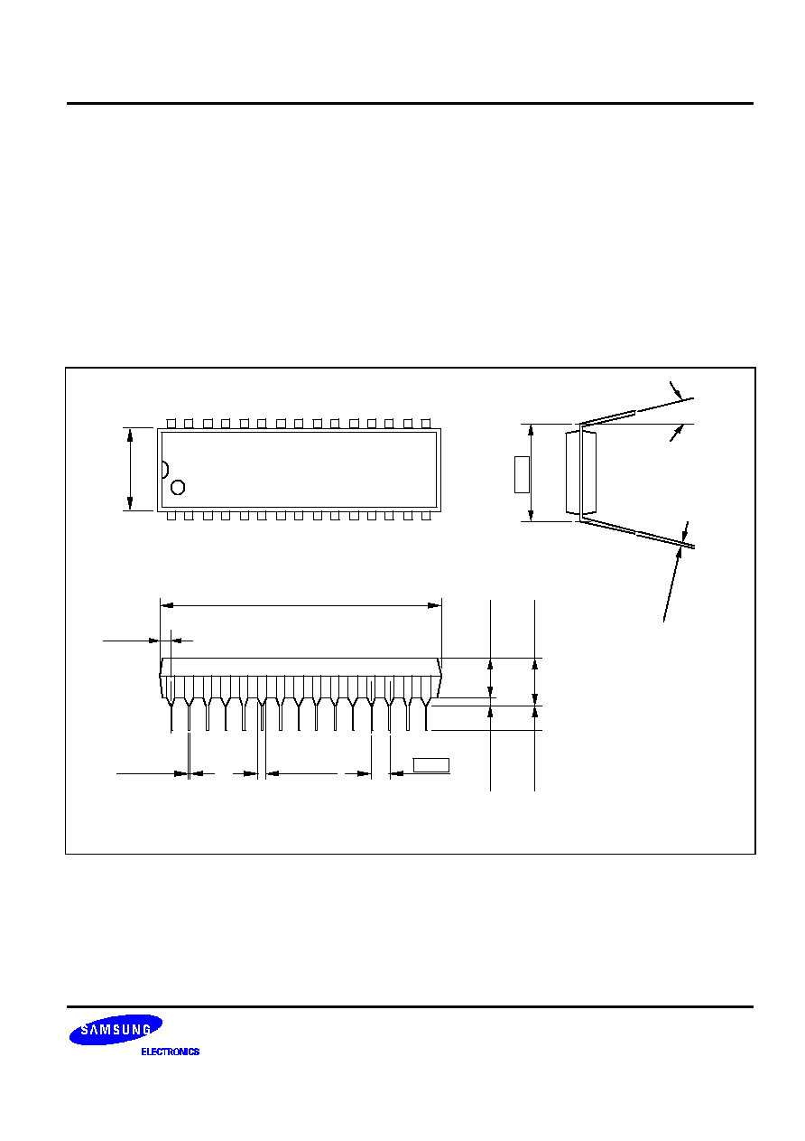
KS57C0502/0504/P0504 MICROCONTROLLER
MECHANICAL DATA
151
15
MECHANICAL DATA
This section contains the following information about the device package:
-- Package dimensions in millimeters
-- Pad diagram
-- Pad/pin coordinate data table
NOTE: Typical dimensions are in millimeters.
30-SDIP-400
8.94 ± 0.2
0.56 ± 0.1
27.48 ± 0.2
0 ~ 15
°
0.25
+0.1 0.05
#1
15
30
16
10.16
(1.30)
1.12 ± 0.1
1.778
0.51MIN
3.81 ± 0.2
3.30 ± 0.3
5.08MAX
Figure 151. 30-SDIP-400 Package Dimensions

MECHANICAL DATA
KS57C0502/0504/P0504 MICROCONTROLLER
152
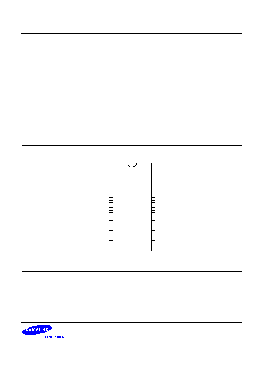
KS57C0502/C0504/P0504 MICROCONTROLLER
KS57P0504 OTP
161
16
KS57P0504 OTP
OVERVIEW
The KS57P0504 single-chip CMOS microcontroller is the OTP (One Time Programmable)
version of the
KS57C0502/C0504 microcontroller. It has an on-chip OTP ROM instead of masked ROM. The EPROM is
accessed by serial data format.
The KS57P0504 is fully compatible with the KS57C0502/C0504, both in function and in pin configuration.
Because of its simple programming requirements, the KS57P0504 is ideal for use as an evaluation chip for the
KS57C0502/C0504.
VDD / VDD
P6.3 / BUZ / SCLK
P6.2 / KS2 / SDAT
P6.1 / KS1
P6.0 / KS0
P5.3
P5.2
P5.1
P5.0
P4.3
P4.2
P4.1
P4.0
P3.2 / CLO
P3.1 / TCLO0
30
29
28
27
26
25
24
23
22
21
20
19
18
17
16
1
2
3
4
5
6
7
8
9
10
11
12
13
14
15
VSS / VSS
Xout
Xin
TEST / TEST
P1.0 / INT0
P1.1 / INT1
RESET
/ RESET
P0.0 /
SCK
P0.1 / SO
P0.2 / SI
P2.0 / CIN0
P2.1 / CIN1
P2.2 / CIN2
P2.3 / CIN3
P3.0 / TCL0
KS57P0504
(30-SDIP)
NOTE: The bolds indicate an OTP pin name.
Figure 161. KS57P0504 Pin Assignments (30-SDIP Package)
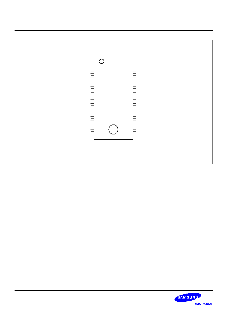
KS57P0504 OTP
KS57C0502/C0504/P0504 MICROCONTROLLER
162
1
2
3
4
5
6
7
8
9
10
11
12
13
14
15
16
32
31
30
29
28
27
26
25
24
23
22
21
20
19
18
17
VSS
Xout
Xin
TEST
P1.0 / INT0
P1.1 / INT1
RESET
NC
P0.0 /
SCK
P0.1 / SO
P0.2 / SI
P2.0 / CIN0
P2.1 / CIN1
P2.2 / CIN2
P2.3 / CIN3
P3.0 / TCL0
VDD / VDD
P6.3 / BUZ /
SCLK
P6.2 / KS2 /
SDAT
P6.1 / KS1
P6.0 / KS0
P5.3
P5.2
P5.1
P5.0
P4.3
P4.2
P4.1
P4.0
NC
P3.2 / CLO
P3.1 / TCLO0
KS57P0504
(32-SOP)
NOTE: The bolds indicate an OTP pin name.
VSS / VSS
Xout
Xin
TEST / TEST
P1.0 / INT0
P1.1 / INT1
RESET
/ RESET
NC
P0.0 /
SCK
P0.1 / SO
P0.2 / SI
P2.0 / CIN0
P2.1 / CIN1
P2.2 / CIN2
P2.3 / CIN3
P3.0 / TCL0
Figure 162. KS57P0504 Pin Assignments (32-SOP Package)
KS57C0502/C0504/P0504 MICROCONTROLLER
KS57P0504 OTP
163
Table 161. Descriptions of Pins Used to Read/Write the EPROM
Main Chip
During Programming
Pin Name
Pin Name
Pin No.
I/O
Function
P6.2
SDAT
28 (30)
I/O
Serial data pin. Output port when reading and
input port when writing. Can be assigned as a
Input / push-pull output port.
P6.3
SCLK
29 (31)
I/O
Serial clock pin. Input only pin.
TEST
V
PP
(TEST)
4 (4)
I
Power supply pin for EPROM cell writing
(indicates that OTP enters into the writing
mode). When 12.5 V is applied, OTP is in
writing mode and when 5 V is applied, OTP is in
reading mode. (Option)
RESET
RESET
7 (7)
I
Chip initialization
V
DD
/ V
SS
V
DD
/ V
SS
30/1 (32/1)
I
Logic power supply pin. VDD should be tied to
+5 V during programming.
NOTE: ( ) means the 32-SOP OTP pin number.
Table 162. Comparison of KS57P0504 and KS57C0502/C0504 Features
Characteristic
KS57P0504
KS57C0502/C0504
Program Memory
4 K-byte EPROM
2 K-byte mask ROM: KS57C0502
4 K-byte mask ROM: KS57C0504
Operating Voltage (V
DD
)
2.0 V to 5.5 V
1.8 V to 5.5V
OTP Programming Mode
V
DD
= 5 V, V
PP
(TEST)=12.5V
Pin Configuration
30 SDIP, 32 SOP
30 SDIP, 32 SOP
EPROM Programmability
User Program one time
Programmed at the factory
OPERATING MODE CHARACTERISTICS
When 12.5 V is supplied to the VPP(TEST) pin of the KS57P0504, the EPROM programming mode is entered.
The operating mode (read, write, or read protection) is selected according to the input signals to the pins listed in
Table 163 below.
Table 163. Operating Mode Selection Criteria
VDD
VPP
(TEST)
REG/
MEM
ADDRESS
(A15-A0)
R/W
MODE
5 V
5 V
0
0000H
1
EPROM read
12.5 V
0
0000H
0
EPROM program
12.5 V
0
0000H
1
EPROM verify
12.5 V
1
0E3FH
0
EPROM read protection
NOTE: "0" means Low level; "1" means High level.
KS57P0504 OTP
KS57C0502/C0504/P0504 MICROCONTROLLER
164
OTP ELECTRICAL DATA
Table 164. Absolute Maximum Ratings
(T
A
= 25
°
C)
Parameter
Symbol
Conditions
Rating
Units
Supply Voltage
V
DD
0.3 to + 6.5
V
Input Voltage
V
I
All I/O ports
0.3 to V
DD
+ 0.3
V
Output Voltage
V
O
0.3 to V
DD
+ 0.3
V
Output Current High
I
O H
One I/O port active
5
mA
All I/O ports active
15
Output Current Low
I
O L
Ports 0, 3, and 6
5
mA
Ports 4 and 5
30
All ports, total
+ 100
Operating Temperature
T
A
40 to + 85
°
C
Storage Temperature
T
stg
65 to + 150
°
C
Table 165. D.C. Electrical Characteristics
(T
A
= 40
°
C to + 85
°
C, V
DD
= 2.0 V to 5.5 V)
Parameter
Symbol
Conditions
Min
Typ
Max
Units
Input High
Voltage
V
IH1
Ports 4 and 5
0.7V
DD
V
DD
V
V
IH2
Ports 0, 1, 2, 3, 6, and
RESET
0.8V
DD
V
DD
V
IH3
X
in
and X
out
V
DD
0.1
V
DD
Input Low
Voltage
V
IL1
Ports 4 and 5
0.3V
DD
V
V
IL2
Ports 0, 1, 2, 3, 6,
and RESET
0.2V
DD
V
IL3
X
in
and X
out
0.1
Output High
Voltage
V
OH
V
DD
= 4.5 V to 5.5 V
I
OH
= 1 mA
Ports 0, 3, 4, 5, 6
V
DD
- 1.0
V
KS57C0502/C0504/P0504 MICROCONTROLLER
KS57P0504 OTP
165
Table 165. D.C. Electrical Characteristics (Continued)
(T
A
= 40
°
C to + 85
°
C, V
DD
= 2.0 V to 5.5 V)
Parameter
Symbol
Conditions
Min
Typ
Max
Units
Output Low
Voltage
V
OL
V
DD
= 4.5 V to 5.5 V
I
OL
= 15 mA
Ports 4, 5
2
V
VDD = 4.5V to 5.5 V
I
OL
= 4.0mA
All output pins except Ports 4, 5
2
Input High
Leakage
Current
I
LIH1
V
IN
= V
DD
All input pins except X
in
and X
out
3
µ
A
I
LIH2
V
IN
= V
DD
X
in
and X
out
20
Input Low
Leakage
Current
I
LIL1
V
IN
= 0 V
All input pins except X
in,
X
out
and
RESET
3
µ
A
I
LIL2
V
IN
= 0 V
X
in
and X
out
20
Output High
Leakage
Current
I
LOH
V
O
= V
DD
All output pins
3
µ
A
Output Low
Leakage
Current
I
LOL
V
O
= 0 V
3
µ
A
Pull-Up
Resistor
R
L1
V
I
= 0 V; V
DD
= 5 V
Port 0, 1, 3, 4, 5, 6
25
50
100
k
V
DD
= 3 V
50
100
200
R
L2
V
DD
= 5 V; V
I
= 0 V;
RESET
100
250
400
V
DD
= 3 V
200
500
800
KS57P0504 OTP
KS57C0502/C0504/P0504 MICROCONTROLLER
166
Table 165. D.C. Electrical Characteristics (Concluded)
(T
A
= 40
°
C to + 85
°
C, V
DD
= 2.0 V to 5.5 V)
Parameter
Symbol
Conditions
Min
Typ
Max
Units
Supply
I
DD1
Run mode; V
DD
= 5.0 V
±
10%
6.0MHz
3.0
8.0
mA
Current
(1)
Crystal oscillator; C1=C2=22pF
4.19MHz
2.0
5.5
V
DD
= 3 V
±
10%
6.0MHz
1.3
4.0
4.19MHz
1.0
3.0
I
DD2
Idle mode; V
DD
= 5.0 V
±
10%
6.0MHz
0.8
2.5
mA
Crystal oscillator; C1=C2=22pF
4.19MHz
0.6
1.8
V
DD
= 3 V
±
10%
6.0MHz
0.6
1.5
4.19MHz
0.4
1.0
I
DD3
Stop mode; V
DD
= 5.0 V
±
10%
0.5
3.0
µ
A
Stop mode; V
DD
= 3.0 V
±
10%
0.3
2.0
NOTES:
1.
D.C. electrical values for Supply current (IDD1 to IDD3) do not include current drawn through internal pull-up registers,
output port drive currents and comparator.
2.
The supply current assumes a CPU clock of fx/4.
CPU CLOCK = 1/n x oscillator frequency (n = 4, 8 or 64)
SUPPLY VOLTAGE (V)
1.05 MHz
15.625 kHz
CPU CLOCK
4.2 MHz
6 MHz
400 kHz
Main Osc. Freq. ( Divided by 4 )
1.5 MHz
1
2
2.7
3
4
5
6
7
Figure 163. Standard Operating Voltage Range
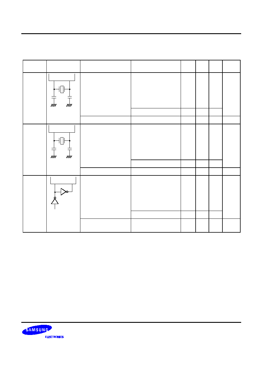
KS57C0502/C0504/P0504 MICROCONTROLLER
KS57P0504 OTP
167
Table 166. Oscillators Characteristics
(T
A
= 40
°
C + 85
°
C, V
DD
= 2.0 V to 5.5 V)
Oscillator
Clock
Configuration
Parameter
Test Condition
Min
Typ
Max
Units
Ceramic
Oscillator
Xin
Xout
C1
C2
Oscillation frequency
(1)
V
DD
= 2.7 V to 5.5 V
0.4
6.0
MHz
V
DD
= 2.0 V to 5.5 V
0.4
4.2
Stabilization time
(2)
V
DD
= 3.0 V
4
ms
Crystal
Oscillator
Xin
Xout
C1
C2
Oscillation frequency
(1)
V
DD
= 2.7 V to 5.5 V
0.4
6.0
MHz
V
DD
= 2.0 V to 5.5 V
0.4
4.2
Stabilization time
(2)
V
DD
= 3.0 V
10
ms
External
Clock
Xin
Xout
X
in
input frequency
(1)
V
DD
= 2.7 V to 5.5 V
0.4
6.0
MHz
V
DD
= 2.0 V to 5.5 V
0.4
4.2
X
in
input high and low
level width (t
XH
, t
XL
)
83.3
1250
ns
NOTES:
1.
Oscillation frequency and X
in
input frequency data are for oscillator characteristics only.
2.
Stabilization time is the interval required for oscillating stabilization after a power-on occurs, or when stop mode is
terminated.
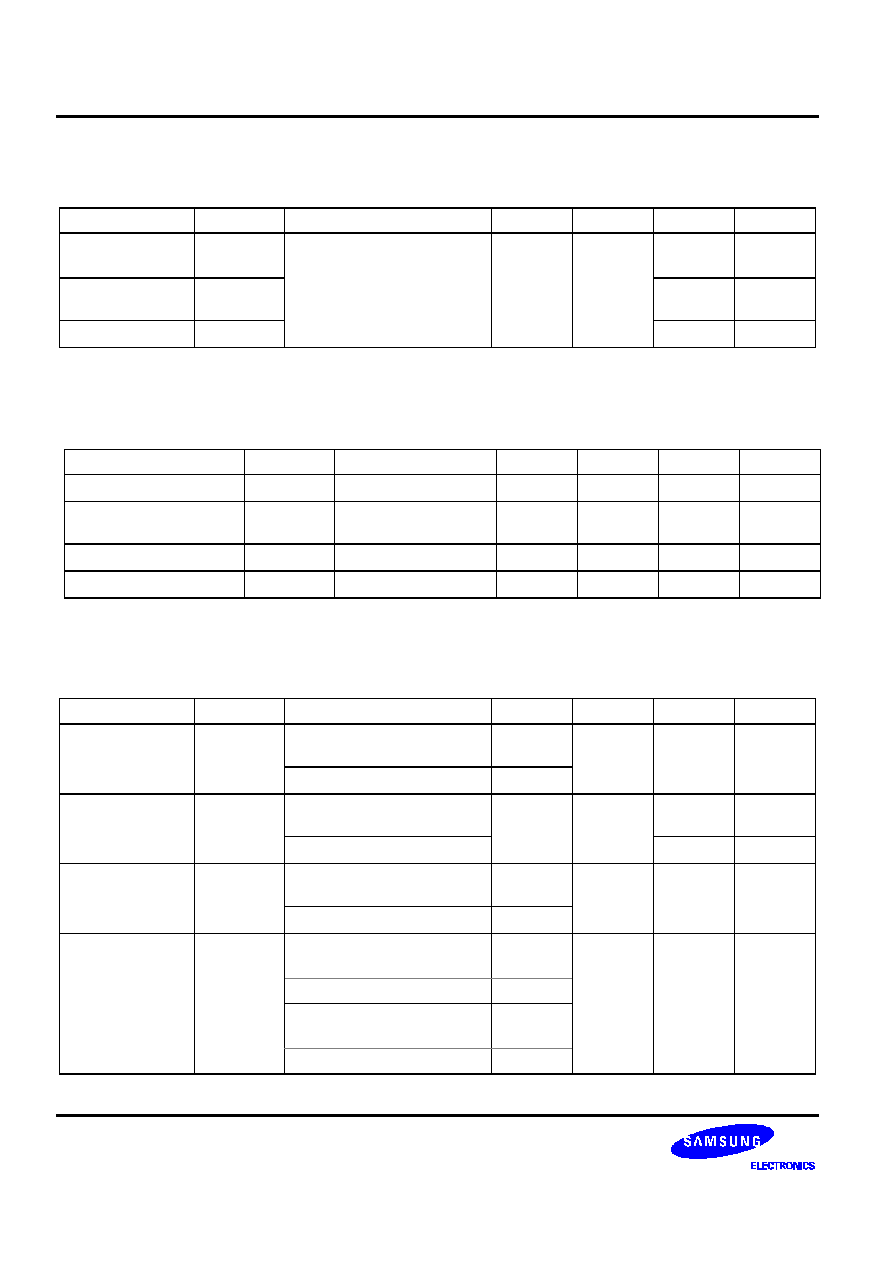
KS57P0504 OTP
KS57C0502/C0504/P0504 MICROCONTROLLER
168
Table 167. Input/Output Capacitance
(T
A
= 25
°
C, V
DD
= 0 V )
Parameter
Symbol
Condition
Min
Typ
Max
Units
Input
Capacitance
C
IN
f = 1 MHz; Unmeasured pins
are returned to V
SS
15
pF
Output
Capacitance
C
OUT
15
pF
I/O Capacitance
C
IO
15
pF
Table 168. Comparator Electrical Characteristics
(T
A
= 40
°
C to + 85
°
C, V
DD
= 4.0 V to 5.5V, V
SS
= 0 V)
Parameter
Symbol
Condition
Min
Typ
Max
Units
Input Voltage Range
0
V
DD
V
Reference Voltage
Range
V
REF
0
V
DD
V
Input Voltage Accuracy
V
CIN
±
150
mV
Input Leakage Current
I
CIN,
I
REF
3
3
µ
A
Table 169. A.C. Electrical Characteristics
(T
A
= 40
°
C to + 85
°
C, V
DD
= 2.0 V to 5.5 V)
Parameter
Symbol
Conditions
Min
Typ
Max
Units
Instruction Cycle
Time
t
CY
V
DD
= 2.7 V to 5.5 V
0.67
64
µ
s
V
DD
= 2.0 V to 5.5 V
0.95
TCL0 Input
Frequency
f
TI
V
DD
= 2.7 V to 5.5 V
0
1.5
MHz
V
DD
= 2.0 V to 5.5 V
1
MHz
TCL0 Input High,
Low Width
t
TIH
,
t
TIL
V
DD
= 2.7 V to 5.5 V
0.48
µ
s
V
DD
= 2.0 V to 5.5 V
1.8
SCK
Cycle Time
t
KCY
V
DD
= 2.7 V to 5.5 V
External
SCK
source
800
ns
Internal
SCK
source
670
V
DD
= 2.0 V to 5.5 V
External
SCK
source
3200
Internal
SCK
source
3800
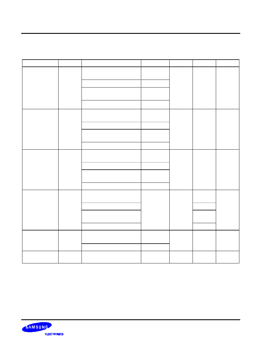
KS57C0502/C0504/P0504 MICROCONTROLLER
KS57P0504 OTP
169
Table 169. A.C. Electrical Characteristics ( Concluded)
(T
A
= 40
°
C to + 85
°
C, V
DD
= 2.0 V to 5.5 V)
Parameter
Symbol
Conditions
Min
Typ
Max
Units
SCK
High, Low
Width
t
KH
, t
KL
V
DD
= 2.7 V to 5.5 V
External
SCK
source
335
ns
Internal
SCK
source
t
KCY
/2 - 50
V
DD
= 2.0 V to 5.5 V
External
SCK
source
1600
Internal
SCK
source
t
KCY
/
2 - 150
SI Setup Time to
SCK
High
t
SIK
V
DD
= 2.7 V to 5.5 V
External
SCK
source
100
ns
Internal
SCK
source
150
V
DD
= 2.0 V to 5.5 V
External
SCK
source
150
Internal
SCK
source
500
SI Hold Time to
SCK
High
t
KSI
V
DD
= 2.7 V to 5.5 V
External
SCK
source
400
ns
Internal
SCK
source
400
V
DD
= 2.0 V to 5.5 V
External
SCK
source
600
Internal
SCK
source
500
Output Delay for
SCK
to SO
t
KSO
(1)
V
DD
= 2.7 V to 5.5 V
External
SCK
source
300
ns
Internal
SCK
source
250
V
DD
= 2.0 V to 5.5 V
External
SCK
source
1000
Internal
SCK
source
1000
Interrupt Input
High, Low Width
t
INTH
,
t
INTL
INT0
(2)
µ
s
INT1, KS0 - KS2
10
RESET
Input Low
Width
t
RSL
Input
10
µ
s
NOTES:
1.
R(1Kohm) and C (100pF) are the load resistance and load capacitance of the SO output line.
2.
Minimum value for INT0 is based on a clock of 2t
CY
or 128 / fx as assigned by the IMOD0 register setting.
KS57P0504 OTP
KS57C0502/C0504/P0504 MICROCONTROLLER
1610
Table 1610. RAM Data Retention Supply Voltage in Stop Mode
(T
A
= 40
°
C to + 85
°
C)
Parameter
Symbol
Conditions
Min
Typ
Max
Unit
Data retention supply voltage
V
DDDR
2.0
5.5
V
Data retention supply current
I
DDDR
V
DDDR
= 2.0 V
0.1
10
µ
A
Release signal set time
t
SREL
0
µ
s
Oscillator stabilization wait
time
(1)
t
WAIT
Released by
RESET
2
17
/ fx
ms
Released by interrupt
(2)
ms
NOTES:
1.
During oscillator stabilization wait time, all CPU operations must be stopped to avoid instability during oscillator start-up.
2.
Use the basic timer mode register (BMOD) interval timer to delay execution of CPU instructions during the wait time.
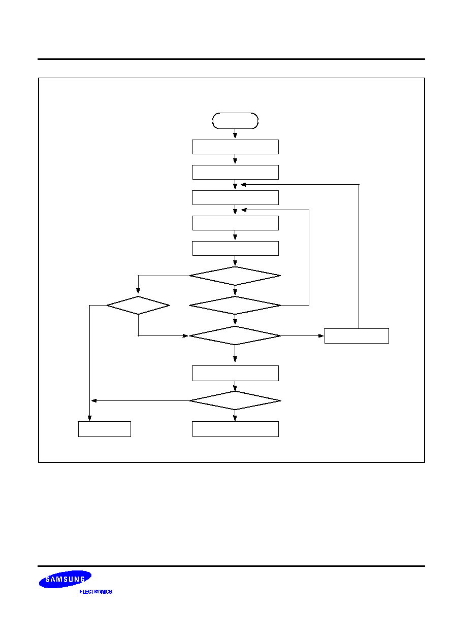
KS57C0502/C0504/P0504 MICROCONTROLLER
KS57P0504 OTP
1611
START
Address= First Location
V
DD
=5V, V
PP
=12.5V
x = 0
Program One 1ms Pulse
Increment X
x = 10
Verify 1 Byte
Last Address
V
DD
= V
PP
= 5 V
Compare All Byte
Device Passed
Increment Address
Verify Byte
Device Failed
PASS
FAIL
NO
FAIL
YES
FAIL
NO
Figure 164. OTP Programming Algorithm

KS57P0504 OTP
KS57C0502/C0504/P0504 MICROCONTROLLER
1612
NOTES

KS57C0502/C0504/P0504 MICROCONTROLLER
DEVELOPMENT TOOLS
171
17
Development Tools
OVERVIEW
Samsung provides a powerful and easy-to-use development support system in turnkey form. The development
support system is configured with a host system, debugging tools, and support software. For the host system, any
standard computer that operates with MS-DOS as its operating system can be used. One type of debugging tool
including hardware and software is provided: the sophisticated and powerful in-circuit emulator, SMDS2+, for
KS57, KS86, KS88 families of microcontrollers. The SMDS2+ is a new and improved version of SMDS2.
Samsung also offers support software that includes debugger, assembler, and a program for setting options.
SHINE
Samsung Host Interface for In-Circuit Emulator, SHINE, is a multi-window based debugger for SMDS2+. SHINE
provides pull-down and pop-up menus, mouse support, function/hot keys, and context-sensitive hyper-linked
help. It has an advanced, multiple-windowed user interface that emphasizes ease of use. Each window can be
sized, moved, scrolled, highlighted, added, or removed completely.
SAMA ASSEMBLER
The Samsung Arrangeable Microcontroller (SAM) Assembler, SAMA, is a universal assembler, and generates
object code in standard hexadecimal format. Assembled program code includes the object code that is used for
ROM data and required SMDS program control data. To assemble programs, SAMA requires a source file and
an auxiliary definition (DEF) file with device specific information.
SASM57
The SASM57 is an relocatable assembler for Samsung's KS57-series microcontrollers. The SASM57 takes a
source file containing assembly language statements and translates into a corresponding source code, object
code and comments. The SASM57 supports macros and conditional assembly. It runs on the MS-DOS operating
system. It produces the relocatable object code only, so the user should link object file. Object files can be linked
with other object files and loaded into memory.
HEX2ROM
HEX2ROM file generates ROM code from HEX file which has been produced by assembler. ROM code must be
needed to fabricate a microcontroller which has a mask ROM. When generating the ROM code (.OBJ file) by
HEX2ROM, the value 'FF' is filled into the unused ROM area upto the maximum ROM size of the target device
automatically.
TARGET BOARDS
Target boards are available for all KS57-series microcontrollers. All required target system cables and adapters
are included with the device-specific target board.
OTPs
One time programmable microcontroller (OTP) for the KS57C0502/C0504 microcontroller and OTP programmer
(Gang) are now available.
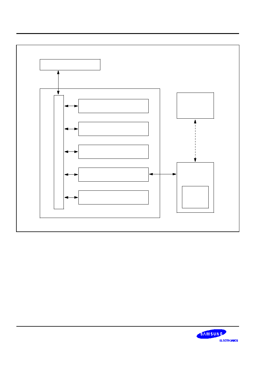
DEVELOPMENT TOOLS
KS57C0502/C0504/P0504 MICROCONTROLLER
172
RAM BREAK/ DISPLAY UNIT
TARGET
APPLICATION
SYSTEM
PROBE
ADAPTER
TB570502A/0504A
TARGET
BOARD
PROM/MTP WRITER UNIT
TRACE/TIMER UNIT
SAM4 BASE UNIT
POWER SUPPLY UNIT
POD
RS-232C
IBM-PC AT or Compatible
BUS
SMDS2+
EVA
CHIP
Figure 171. SMDS Product Configuration (SMDS2+)
KS57C0502/C0504/P0504 MICROCONTROLLER
DEVELOPMENT TOOLS
173
TB570502A/0504A TARGET BOARD
The TB570502A/0504A target board is used for the KS57C0502/C0504/P0504 microcontroller. It is supported by
the SMDS2+ development system.
SM1253A
TB570502A/0504A
3
0-PIN CONNECTOR
1
30
15
16
1
25
EXTERNAL
TRIGGERS
CH1
CH2
OFF
ON
To User_Vcc
RESET
+
STOP
+
IDLE
100-PIN CONNECTOR
J101
100 QFP
KS57E0500
EVA CHIP
1
30
74HC11
XTAL
MDS
XI
Figure 172. TB570502A/TB570504A Target Board Configuration
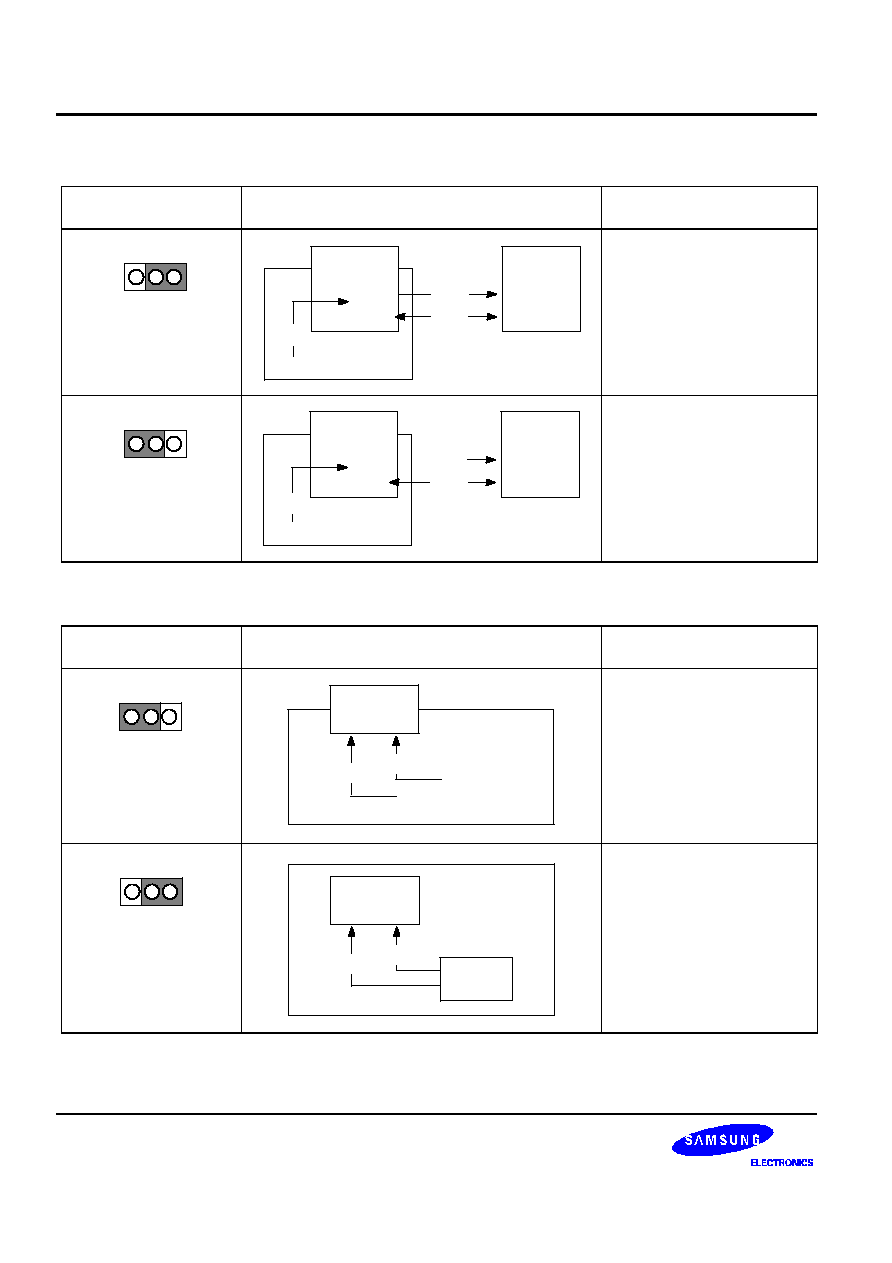
DEVELOPMENT TOOLS
KS57C0502/C0504/P0504 MICROCONTROLLER
174
Table 171. Power Selection Settings for TB570502A/TB570504A
'To User_Vcc' Settings
Operating Mode
Comments
To User_Vcc
ON
OFF
V
CC
TARGET
SYSTEM
SMDS2/SMDS2+
V
SS
V
CC
TB570502A
/0504A
The SMDS2/SMDS2+
supplies V
CC
to the target
board (evaluation chip) and
the target system.
To User_Vcc
ON
OFF
TARGET
SYSTEM
External
V
CC
SMDS2/SMDS2+
V
CC
V
SS
TB570502A
/0504A
The SMDS2/SMDS2+
supplies V
CC
only to the
target board (evaluation chip).
The target system must have
its own power supply.
Table 172. Clock Selection Settings for TB570502A/TB570504A
Sub Clock Setting
Operating Mode
Comments
XTI
XTAL
MDS
XT
IN
SMDS2/SMDS2+
EVA CHIP
KS57E 0500
XT
OUT
No connection
100 pin connector
Set the XTI switch to "MDS"
when the target board is
connected to the
SMDS2/SMDS2+.
XTI
XTAL
MDS
XT
IN
TARGET BOARD
EVA CHIP
KS57E0500
XT
OUT
XTAL
Set the XTI switch to "XTAL"
when the target board is used
as a standalone unit, and is
not connected to the
SMDS2/SMDS2+.
KS57C0502/C0504/P0504 MICROCONTROLLER
DEVELOPMENT TOOLS
175
Table 173. Using Single Header Pins as the Input Path for External Trigger Sources
Target Board Part
Comments
EXTERNAL
TRIGGERS
CH1
CH2
Connector from
external trigger
sources of the
application system
You can connect an external trigger source to one of the two external
trigger channels (CH1 or CH2) for the SMDS2+ breakpoint and trace
functions.
IDLE LED
This LED is ON when the evaluation chip (KS57E0500) is in idle mode.
STOP LED
This LED is ON when the evaluation chip (KS57E0500) is in stop mode.
DEVELOPMENT TOOLS
KS57C0502/C0504/P0504 MICROCONTROLLER
176
J101
V
SS
Xout
Xin
TEST
P1.0/INT0
P1.1/INT1
RESET
P0.0/
SCK
P0.1/SO
P0.2/SI
P2.0/CIN0
P2.1/CIN1
P2.2/CIN2
P2.3/CIN3
P3.0/TCL0
V
DD
P6.3/BUZ/ SCLK
P6.2/KS2/SDAT
P6.1/KS1
P6.0/KS0
P5.3
P5.2
P5.1
P5.0
P4.3
P4.2
P4.1
P4.0
P3.2/CLO
P3.1/TCLO0
3
0-PIN DIP CONNECTOR
1
2
3
4
5
6
7
8
9
10
11
12
13
14
15
30
29
28
27
26
25
24
23
22
21
20
19
18
17
16
Figure 173. 30-Pin Connector for TB570502A/TB570504A
3
0-PIN DIP CONNECTOR
TARGET BOARD
TARGET SYSTEM
Target Cable for 32-SDIP Socket
Part Name: AP30SD-C
Order Code: SM6519
J101
1
30
15
16
1
30
15
16
Figure 174. TB570502A/TB570504A Adapter Cable for 30-SDIP Package (KS57C0502/C0504/P0504)