 | –≠–ª–µ–∫—Ç—Ä–æ–Ω–Ω—ã–π –∫–æ–º–ø–æ–Ω–µ–Ω—Ç: KS58015 | –°–∫–∞—á–∞—Ç—å:  PDF PDF  ZIP ZIP |
KS58015 DTMF DIALER FOR BINARY DATA-IN
INTRODUCTION
The KS58015 is a DTMF dialer for 4 bit binary data input from
microprocessor. When the tone enable input low, the oscillator is in-
hibited and the device is in a low power consumption at standby mode.
On the low to high transition of tone enable, data is latched into the
device and selected the standard DTMF signals.
The N-channel open drain output provides a MUTE output during tone
generation.
FEATURES
∑
Direct interface with microprocessor
∑
Generates 16 standard tones
∑
Uses inexpensive TV crystal or ceramic resonator
(3.579545MHz)
∑
Very low total harmonic distortion
∑
Low power standby mode
∑
Binary data inputs with latches
∑
Wide Operating Voltage : 2.5 ~ 8.0V
BLOCK DIAGRAM
Fig.1
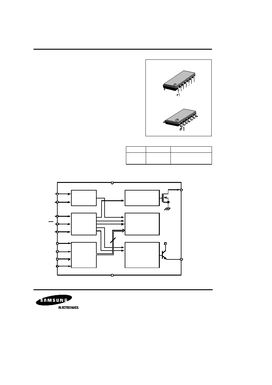
Device
Package
Operating Temperature
KS58015N
KS58015D
14-DIP-300
14-SOP-225B
OSC
CONTROL
CIRCUIT
DATA
LATCH &
DECODER
MUTE LOGIC
ROW & COLUMN
TONE COUNTER
D/A
CONVER TER &
MIXING
TONE OUT
MUTE
OSC IN
OSC OUT
TEN
ST
GS
D0
D1
D2
D3
V
DD
V
S S
4
- 30
∞
C ~ + 70
∞
C
14-DIP-300
14-SOP-225B
ORDERING INFORMATION
KS58015 DTMF DIALER FOR BINARY DATA-IN
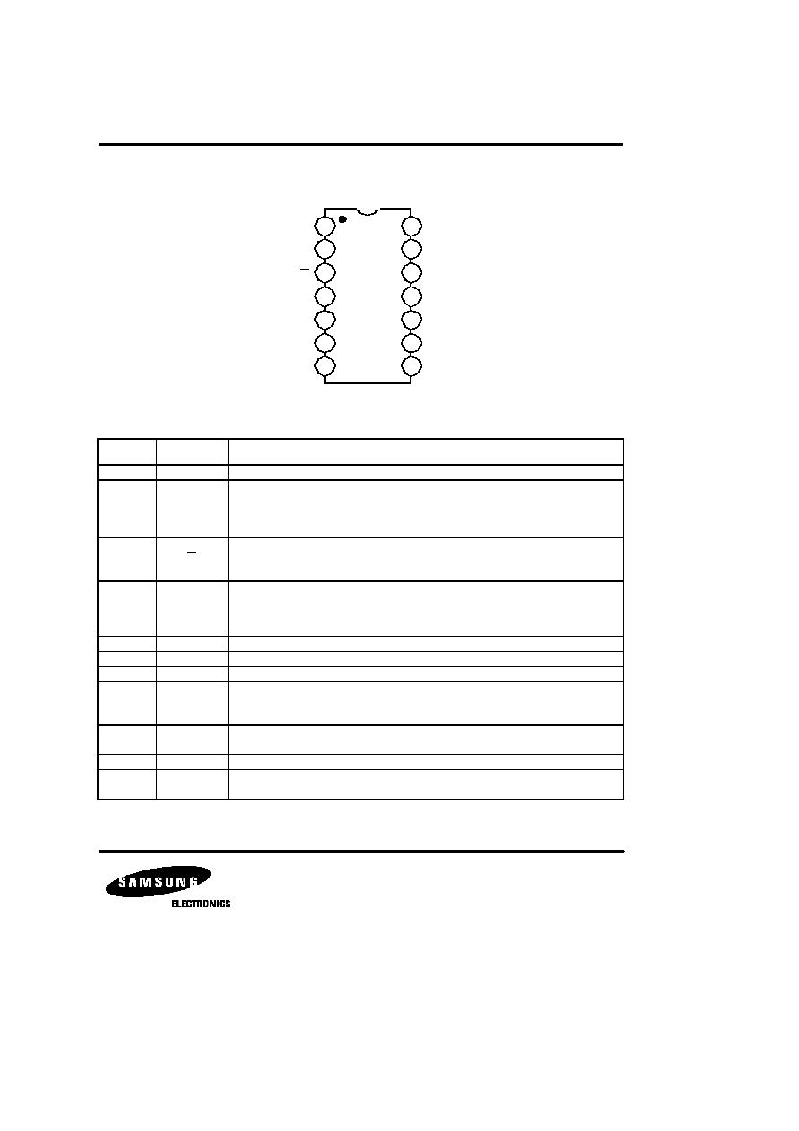
PIN CONFIGURATION
Fig. 2
PIN DESCRIPTION
1
2
3
4
5
6
7
8
9
10
11
12
13
14
KS58015
V
DD
TEN
ST
GS
V
SS
OSC IN
OSC OUT
MUTE
TONE OUT
D3
D2
D1
D0
NC
Pin No
Symbol
Descriptions
1
V
DD
Positive supply input
2
TEN
Tone enable input. An internal pull-up resistor is in a chip. When this pin connects to
logic `low', the oscillator is inhibited and the tone generators and output transistor are
turned off. A low to high transition on this pin latches in data from D0 ~ D3, and tone
generation continues until this pin is connected `low' again.
3
ST
Single tone enable. An internal pull-up resistor is in a chip. When this pin connects
to logic `low', the device is in a single tone mode. For normal operation, connects this
pin to V
DD
or open-circuit.
4
GS
Group selection input. This pin is used to select the high group or low group fre-
quency, when the device is in single tone mode. An internal pull-up resistor is in a
chip. When this pin connects to V
DD
or open, the high group will be generated, and when
connects to V
SS
, the low group will be generated.
5
V
SS
Negative supply input
6
OSC IN
Oscillator input
7
OSC OUT
Oscillator output
8
MUTE
N-channel open drain output.
This pin is a logic high state, when the tone enable pin is a high state.
This pin goes a logic low state, when the tone enable pin is a low state.
9, 10,
11, 12
D0, D1,
D2, D3
DATA-INPUTS. These are the inputs for binary-coded data, which is latched in on
the rising edge of the tone enable signal.
13
N.C
No connection.
14
Tone out
This output is the open emitter of a NPN transistor. When an external load resistor
is connected from this pin to V
SS
, the tone generates on the tone enable pin = `High'.
KS58015 DTMF DIALER FOR BINARY DATA-IN
ABSOLUTE MAXIMUM RATINGS
ELECTRICAL CHARACTERISTICS
(V
SS
= 0V, 2V<V
DD
<8V, f
OSC
= 3.579545MHz, Ta = 25
∞
C, unless otherwise noted)
APPLICATION INFORMATION
FUNCTION DESCRIPTION
When tone enable input is low, oscillator is inhibited, being allowed to low power standby mode
since transistor goes to
turn off state, so D0 ~ D3 input data is ignored.
However if tone enable input goes from low to high, input data is latched and tone output is enabled, and it is correspond
to data input.
This device is designed with 14 levels, 28 segments in each single-tone. The column tone is pre-emphasized 2dB than
the row tone.
TABLE1. SINGLE TONE FREQUENCY
Characteristic
Symbol
Value
Unit
Supply Voltage
MUTE Voltage
Input Voltage
Power Dissipation
Operating Temperature
Storage Temperature
V
DD
V
I (MUTE)
V
I
P
D
T
OPR
T
STG
9
9
V
DD
+ 0.3 ~ V
SS
- 0.3
500
- 30 ~ + 70
- 55 ~ + 125
V
V
V
mW
∞
C
∞
C
Characteristic
Symbol
Test Conditions
Min
Typ
Max
Unit
Operating Voltage Range
V
DD
2.0
8.0
V
Operating Current
I
DD
V
DD
= 3.0V, MUTE Open
1.5
mA
Standby Current
I
SB
R
L
= 10K, D0~D3 open, V
DD
= 3.0V
50
100
µ
A
Input Pull-up Resistance
R
I (PULL)
DI0 ~ DI3, TEN
100
K
V
IL
V
SS
0.2V
DD
V
V
IH
0.8V
DD
V
DD
V
I
OL (MUTE)
V
DD
= 3V, V
O
= 0.5, TEN = LOW
0.5
1.5
mA
I
OH (MUTE)
V
DD
= 3V, V
O
= V
DD
, TEN = HIGH
1
2
µ
A
Tone Output Level
V
O (TONE)
V
DD
= 3V, R
L
= 5K
, Row Tone
-14
-11
dBV
Ratio of Column to Row
dB
CR
V
DD
= 3V, R
L
= 5 K
1
2
3
dB
THD (Dual Tone)
THD
1MHz Bandwidth, V
DD
= 5V, R
L
=5K
-20
dB
Oscillator Start-up Time
t
ST (OSC)
90% Amplitudes, V
DD
= 3.0V
4
mS
Data Set-up Time
t
SU (DATA)
V
DD
= 3.0V
200
nS
Data Hold Time
t
H (DATA)
V
DD
= 3.0V
200
nS
Data Duration
t
W (DATA)
V
DD
= 3.0V
600
nS
Tone Group
Standard DTMF (Hz)
Tone Output Actual Frequency
% Deviation from Standard
ROW 1
ROW 2
ROW 3
ROW 4
COLUMN 1
COLUMN 2
COLUMN 3
COLUMN 4
697
770
852
941
1209
1336
1477
1633
699.13
766.17
845.43
947.97
1215.89
1331.67
1471.85
1645.01
+ 0.31
- 0.50
- 0.54
+ 0.74
+ 0.57
- 0.33
- 0.35
+ 0.75
Input Voltage
Output Current (MUTE)
DI0 ~ DI3, TEN
KS58015 DTMF DIALER FOR BINARY DATA-IN
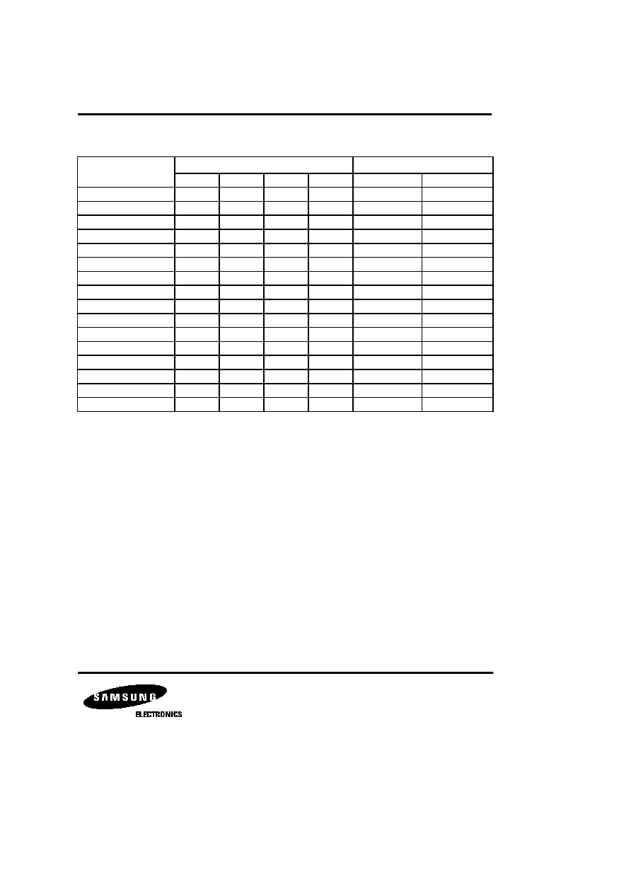
TABLE 2. FUNCTION TABLE
Key Board
Data Input
Tone Output
Equivalent
D3
D2
D1
D0
f
L
(Hz)
f
H
(Hz)
1
0
0
0
1
697
1209
2
0
0
1
0
697
1336
3
0
0
1
1
697
1477
4
0
1
0
0
770
1209
5
0
1
0
1
770
1336
6
0
1
1
0
770
1477
7
0
1
1
1
852
1209
8
1
0
0
0
852
1336
9
1
0
0
1
852
1477
0
1
0
1
0
941
1336
*
1
0
1
1
941
1209
#
1
1
0
0
941
1477
A
1
1
0
1
697
1633
B
1
1
1
0
770
1633
C
1
1
1
1
852
1633
D
0
0
0
0
941
1633