
KS86C4302/C4304/P4304
PRODUCT OVERVIEW
1-1
1
PRODUCT OVERVIEW
SAM87RI PRODUCT FAMILY
Samsung's SAM87Ri family of 8-bit single-chip CMOS microcontrollers offers a fast and efficient CPU, a wide
range of integrated peripherals, and various mask-programmable ROM sizes.
A address/data bus architecture and a large number of bit-configurable I/O ports provide a flexible programming
environment for applications with varied memory and I/O requirements. Timer/counters with selectable operating
modes are included to support real-time operations.
KS86C4302/C4304 MICROCONTROLLER
The KS86C4302/C4304 single-chip 8-bit microcontroller is fabricated using an advanced CMOS process. It is
built around the powerful SAM87Ri CPU core. The KS86C4302/C4304 is a versatile microcontroller, with its A/D
converter, timer, PWM, and SIO it can be used in a wide range of general purpose applications.
Stop and Idle power-down modes were implemented to reduce power consumption. To increase on-chip register
space, the size of the internal register file was logically expanded. The KS86C4302/C4304 have 2-Kbytes or 4-
Kbytes of program memory on-chip (ROM) and 112-bytes of general purpose register area RAM.
Using the SAM87Ri design approach, the following peripherals were integrated with the SAM87Ri core:
-- Three configurable I/O ports (13 pins)
-- Five interrupt sources with one vector and one interrupt level
-- One 8-bit timer/counter with time interval mode
-- Analog to digital converter with five input channels and 10-bit resolution
-- One synchronous SIO module
-- One 12-bit PWM output
The KS86C4302/C4304 microcontroller is ideal for use in a wide range of electronic applications requiring simple
timer/counter, PWM, ADC, and SIO. KS86C4302/C4304 is available in a 20/18/16-pin DIP and a 20-pin SOP
package.
OTP
The KS86P4304 is an OTP (One Time Programmable) version of the KS86C4302/C4304 microcontroller. The
KS86P4304 has on-chip 4-Kbyte one-time-programmable EPROM instead of masked ROM. The KS86P4304 is
fully compatible with the KS86C4302/C4304, in function, in D.C. electrical characteristics and in pin configuration.

PRODUCT OVERVIEW
KS86C4302/C4304/P4304
1-2
FEATURES
CPU
�
SAM87RI CPU core
Memory
�
2/4-Kbyte internal program memory (ROM)
�
112-byte general purpose register area (RAM)
Instruction Set
�
41 instructions
�
The SAM87RI core provides all the SAM87 core
instruction except the word-oriented instruction,
multiplication, division, and some one-byte
instruction.
Instruction Execution Time
�
600 ns at 10 MHz f
OSC
(minimum cycles)
�
375 ns at 16 MHz f
OSC
(minimum cycles)
Interrupts
�
5 interrupt sources with one vector and one level
interrupt structure
General I/O
�
Two I/O ports (Toatal 13 pins)
�
One output only port (port 2)
�
Bit programmable ports
Serial I/O
�
One synchronius serial I/O module
�
Selectable transmit and receive rates
Built-in reset Circuit (LVD)
�
Low voltage detector for safe reset
Timer/Counters
�
One 8-bit basic timer for watchdog function
�
One 8-bit timer/counter for the time interval
mode
PWM Module
�
12-bit PWM 1-ch (Max: 250 kHz)
�
6-bit base + 6-bit extension frame
A/D Converter
�
Five analog input pins
�
10-bit conversion resolution
Buzzer Frequency Range
�
200 Hz to 20 kHz signal can be generated
Oscillation Frequency
�
1 MHz to 16 MHz external crystal oscillator
�
Maximum 16 MHz CPU clock
�
4 MHz RC oscillator
Operating Temperature Range
�
- 40
�
C to + 85
�
C
Operating Voltage Range
�
3.0 V to 5.5 V
OTP Interface Protocol Spec
�
Serial OTP
Package Types
�
20-pin DIP-300
�
20-pin SOP-375
�
18-pin DIP-300
�
16-pin DIP-300

KS86C4302/C4304/P4304
PRODUCT OVERVIEW
1-3
BLOCK DIAGRAM
SAM87RI CPU
P0.0-P0.3
BUZ, PWM, INT0, INT1
I/O Port and
Interrupt Control
2-KB ROM
4-KB ROM
112-Byte
Register File
Port 0
Port 1
P1.0-P1.4
ADC0-ADC4
SCK, SO, SI, CLO
Port 2
SIO
Timer 0
BUZ
ADC
PWM
OSC
Basic
Timer
P2.0/SCK
P2.1/SO
P2.2
P2.3
SCK (P1.3 or P2.0)
SO (P1.2 or P2.1)
SI (P1.1)
X
IN
X
OUT
P0.2/T0CK
P0.0/BUZ
ADC0-ADC4
P0.1/PWM
Figure 1-1. Block Diagram

PRODUCT OVERVIEW
KS86C4302/C4304/P4304
1-4
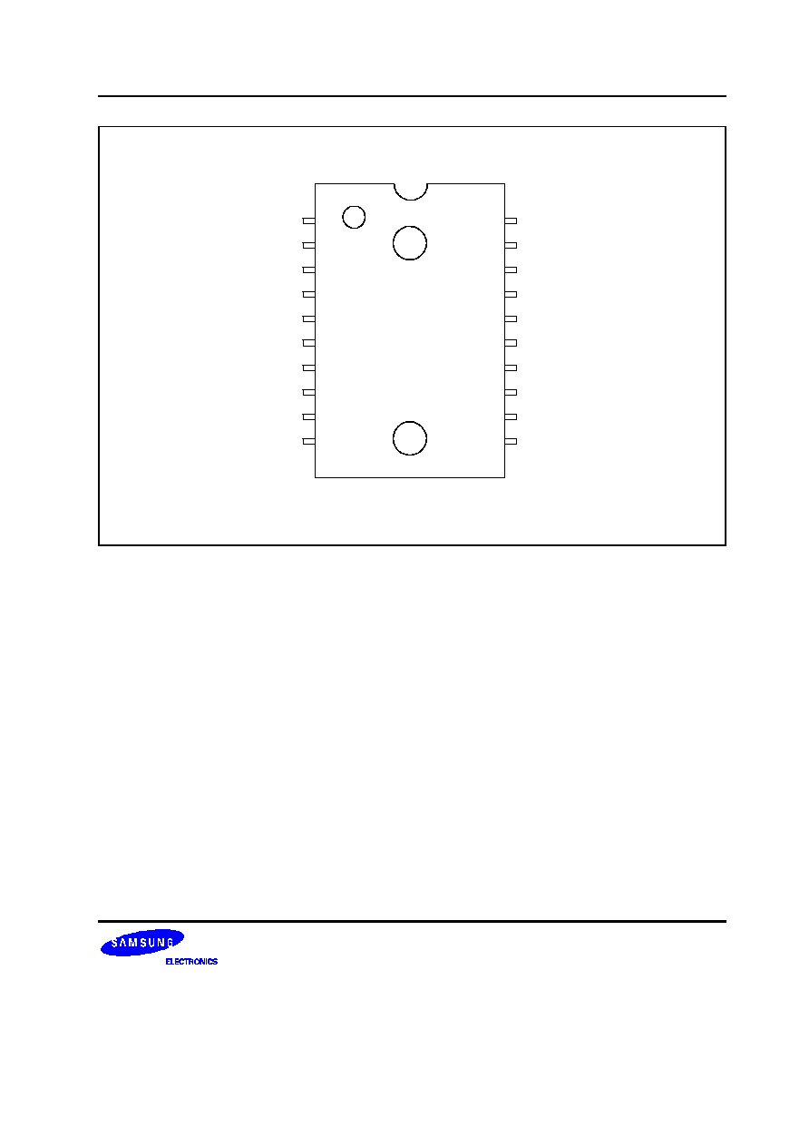
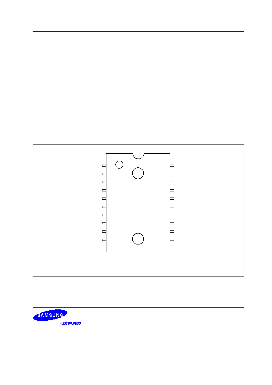
PIN ASSIGNMENTS
KS86C4302/
4304
(TOP VIEW)
V
DD
P0.3/INT1
P1.0/ADC0
P1.1/ADC1/SI
P1.2/ADC2/SO
P1.3/ADC3/SCK
P1.4/ADC4/CLO
AV
REF
P2.1/SO
P2.3
20
19
18
17
16
15
14
13
12
11
V
SS
X
IN
X
OUT
TEST
P0.2/T0CK/INT0
P0.1/PWM
RESET
P0.0/BUZ
P2.0/SCK
P2.2
1
2
3
4
5
6
7
8
9
10
Figure 1-2. Pin Assignment Diagram (20-Pin DIP Package)
KS86C4302/C4304/P4304
PRODUCT OVERVIEW
1-5
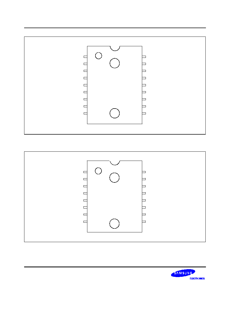
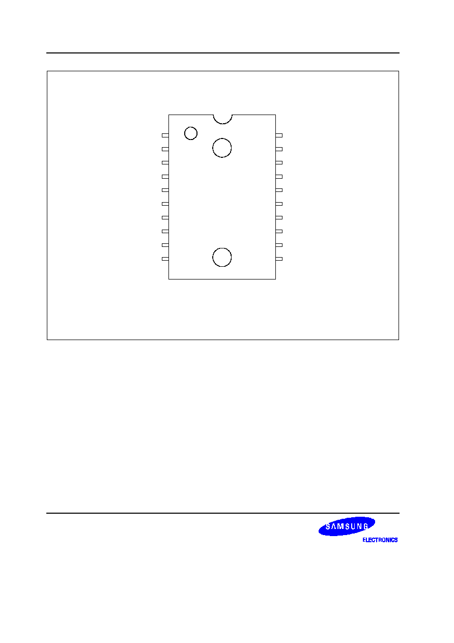
KS86C4302/
4304
(TOP VIEW)
V
DD
P0.3/INT1
P1.0/ADC0
P1.1/ADC1/SI
P1.2/ADC2/SO
P1.3/ADC3/SCK
P1.4/ADC4/CLO
AV
REF
P2.1/SO
P2.3
20
19
18
17
16
15
14
13
12
11
V
SS
X
IN
X
OUT
TEST
P0.2/T0CK/INT0
P0.1/PWM
RESET
P0.0/BUZ
P2.0/SCK
P2.2
1
2
3
4
5
6
7
8
9
10
Figure 1-3. Pin Assignment Diagram (20-Pin SOP Package)
PRODUCT OVERVIEW
KS86C4302/C4304/P4304
1-6
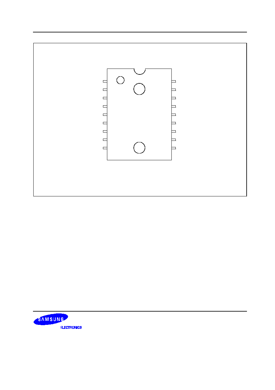
KS86C4302/
4304
(TOP VIEW)
V
DD
P0.3/INT1
P1.0/ADC0
P1.1/ADC1/SI
P1.2/ADC2/SO
P1.3/ADC3/SCK
P1.4/ADC4/CLO
AV
REF
P2.1/SO
18
17
16
15
14
13
12
11
10
V
SS
X
IN
X
OUT
TEST
P0.2/T0CK/INT0
P0.1/PWM
RESET
P0.0/BUZ
P2.0/SCK
1
2
3
4
5
6
7
8
9
Figure 1-4. Pin Assignment Diagram (18-Pin DIP Package)
V
SS
X
IN
X
OUT
TEST
P0.2/T0CK/INT0
P0.1/PWM
RESET
P0.0/BUZ
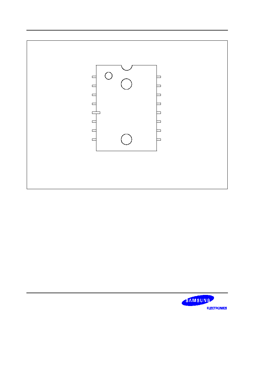
KS86C4302/
4304
(TOP VIEW)
V
DD
P0.3/INT1
P1.0/ADC0
P1.1/ADC1/SI
P1.2/ADC2/SO
P1.3/ADC3/SCK
P1.4/ADC4/CLO
AV
REF
16
15
14
13
12
11
10
9
1
2
3
4
5
6
7
8
Figure 1-5. Pin Assignment Diagram (16-Pin DIP Package)
KS86C4302/C4304/P4304
PRODUCT OVERVIEW
1-7
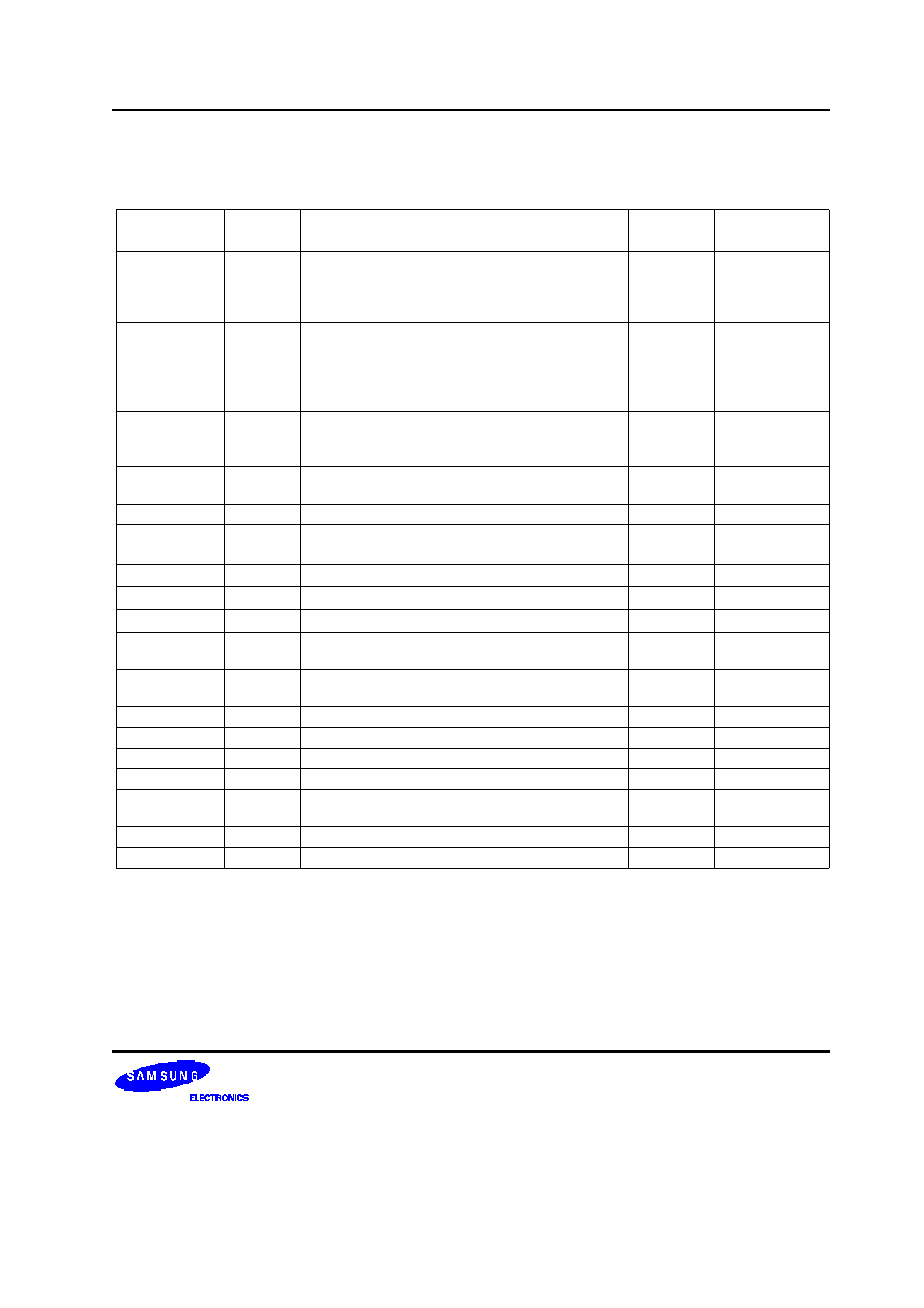
PIN DESCRIPTIONS
Table 1-1. KS86C4302/C4304 Pin Descriptions
Pin
Names
Pin
Type
Pin
Description
Circuit
Type
Share
Pins
P0.0-P0.3
I/O
Bit-programmable I/O port for Schmitt trigger
input or push-pull, open-drain output. Pull-up
resistors are assignable by software. Port 0 pins
can also be used as alternative function.
E
BUZ
PWM
INT0/T0CK
INT1
P1.0-P1.4
I/O
Bit-programmable I/O port for Schmitt trigger
input or push-pull, open-drain output. Pull-up
resistors are assignable by software. Port 1 pins
can also be used as alternative function.
E-1
ADC0-ADC4
SI
SO
SCK
CLO
P2.0-P2.3
O
Push-pull or open-drain output port. Pull up
resistors are assignable by software. Port 2.0-2.1
pins can also be used as alternative function.
E-2
SCK
SO
X
IN
, X
OUT
�
Crystal/ceramic, or RC oscillator signal for
system clock.
�
�
RESET
I
System
RESET
signal input pin.
B
�
TEST
I
Test signal input pin (for factory use only: must be
connected to V
SS
)
�
�
V
DD,
V
SS
�
Voltage input pin and ground
�
�
AV
REF
�
A/D converter reference voltage input and ground
�
�
AV
SS
Bonded to V
SS
internally
SCK
I/O
Serial interface clock I/O
E-1
E-2
P1.3 or
P2.0
SO
O
Serial data output
E-1
E-2
P1.2 or
P2.1
SI
I
Serial data input
E-1
P1.1
CLO
O
System clock output port
E-1
P1.4
BUZ
O
200 Hz- 20 kHz frequency output for buzzer sound
E
P0.0
PWM
O
12-bit PWM output
E
P0.1
INT0-INT1
I
External interrupt input port
E
P0.2
P0.3
T0CK
I
Timer 0 external clock input
E
P0.2
ADC0-ADC4
I
A/D converter input
E-1
P1.0-P1.4
PRODUCT OVERVIEW
KS86C4302/C4304/P4304
1-8
PIN CIRCUITS
P-Channel
N-Channel
In
V
DD
Figure 1-6. Pin Circuit Type A
In
V
DD
Pull-Up
Resistor
Figure 1-7. Pin Circuit Type B
P-Channel
N-Channel
V
DD
Out
Output
DIsable
Data
Figure 1-8. Pin Circuit Type C
I/O
Output
DIsable
Data
Circuit
Type C
Pull-up
Enable
V
DD
Data
P-Channel
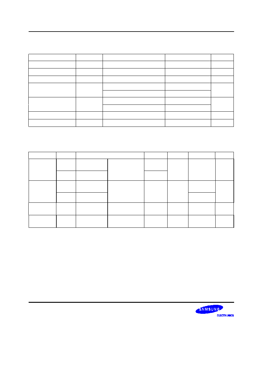
Figure 1-9. Pin Circuit Type D
KS86C4302/C4304/P4304
PRODUCT OVERVIEW
1-9
N-CH
V
DD
P-CH
Output
DIsable
Output
Data
Open-Drain
Input
Pull-up
Enable
V
DD
I/O
Pull-up
Resistor
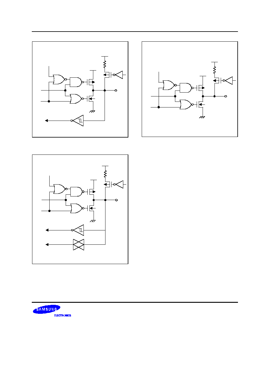
Figure 1-10. Pin Circuit Type E
Analog
Input
N-CH
V
DD
P-CH
Output
DIsable
Output
Data
Open-Drain
Digital
Input
Pull-up
Enable
V
DD
I/O
Pull-up
Resistor
Figure 1-11. Pin Circuit Type E-1
N-CH
V
DD
P-CH
Output
DIsable
Output
Data
Open-Drain
Pull-up
Enable
V
DD
I/O
Pull-up
Resistor
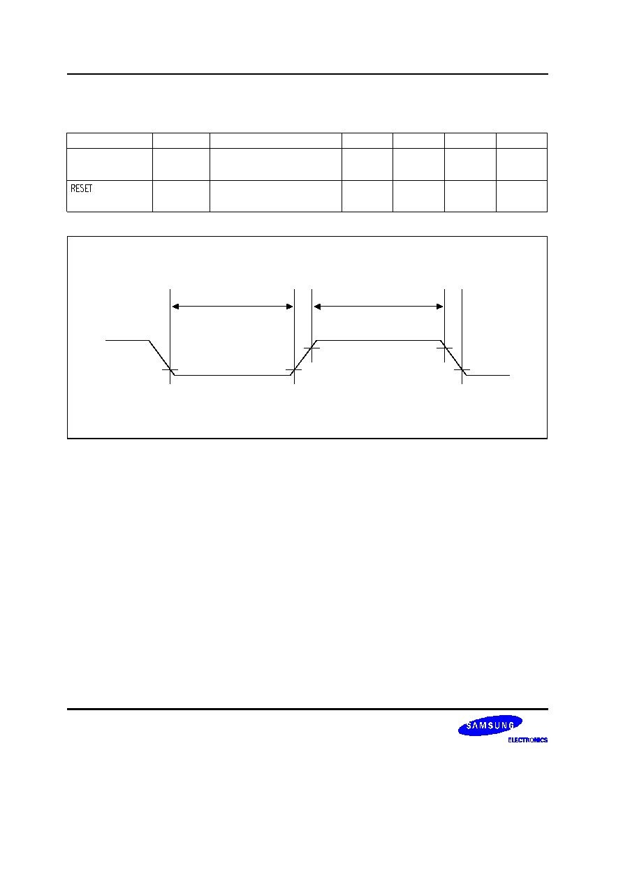
Figure 1-12. Pin Circuit Type E-2

PRODUCT OVERVIEW
KS86C4302/C4304/P4304
1-10
NOTES

KS86C4302/C4304/P4304
ELECTRICAL DATA
14-1
14
ELECTRICAL DATA
OVERVIEW
In this section, the following KS86C4302/C4304 electrical characteristics are presented in tables and graphs:
-- Absolute maximum ratings
-- D.C. electrical characteristics
-- A.C. electrical characteristics
-- Input Timing Measurement Points
-- Oscillator characteristics
-- Oscillation stabilization time
-- Operating Voltage Range
-- Schmitt trigger input characteristics
-- Data retention supply voltage in Stop mode
-- Stop mode release timing when initiated by a
RESET
-- A/D converter electrical characteristics
-- LVD circuit characteristics
-- LVD reset Timing
-- Serial I/O timing characteristics
-- Serial data transfer timing
ELECTRICAL DATA
KS86C4302/C4304/P4304
14-2
Table 14-1. Absolute Maximum Ratings
(T
A
= 25
�
C)
Parameter
Symbol
Conditions
Rating
Unit
Supply voltage
V
DD
�
- 0.3 to + 6.5
V
Input voltage
V
I
All input ports
- 0.3 to V
DD
+ 0.3
V
Output voltage
V
O
All output ports
- 0.3 to V
DD
+ 0.3
V
Output current high
I
OH
One I/O pin active
- 25
mA
All I/O pins active
- 80
Output current low
I
OL
One I/O pin active
+ 30
mA
All I/O pins active
+ 150
Operating temperature
T
A
�
- 40 to + 85
�
C
Storage temperature
T
STG
�
- 65 to + 150
�
C
Table 14-2. DC Electrical Characteristics
(T
A
= � 40
�
C to + 85
�
C, V
DD
= 3.0 V to 5.5 V)
Parameter
Symbol
Conditions
Min
Typ
Max
Unit
Input high
voltage
V
IH1
Ports 0, 1, and
RESET
V
DD
= 3.0 to 5.5 V
0.8 V
DD
�
V
DD
V
V
IH2
X
IN
and X
OUT
V
DD
- 0.1
Input low
voltage
V
IL1
Ports 0, 1, and
RESET
V
DD
= 3.0 to 5.5 V
�
�
0.2 V
DD
V
V
IL2
X
IN
and X
OUT
0.1
Output high
voltage
V
OH
I
OH
= - 10 mA
ports 0, 1, 2
V
DD
= 4.5 to 5.5 V
V
DD
- 1.5
V
DD
- 0.4
�
V
Output low
voltage
V
OL
I
OL
= 25 mA
port 0, 1, and 2
V
DD
= 4.5 to 5.5 V
�
0.4
2.0
V

KS86C4302/C4304/P4304
ELECTRICAL DATA
14-3
Table 14-2. DC Electrical Characteristics (Continued)
(T
A
= � 40
�
C to + 85
�
C, V
DD
= 3.0 V to 5.5 V)
Parameter
Symbol
Conditions
Min
Typ
Max
Unit
Input high leakage
current
I
LIH1
All inputs except I
LIH2
V
IN
= V
DD
�
�
1
uA
I
LIH2
X
IN
,
X
OUT
V
IN
= V
DD
20
Input low leakage
current
I
LIL1
All inputs except
I
LIL2
and
RESET
V
IN
= 0 V
�
�
-1
uA
I
LIL2
X
IN
, X
OUT
V
IN
= 0 V
-20
Output high
leakage current
I
LOH
All outputs
V
OUT
= V
DD
�
�
2
uA
Output low
leakage current
I
LOL
All outputs
V
OUT
= 0 V
�
�
-2
uA
Pull-up resistors
R
P
V
IN
= 0 V
Ports 0-2
V
DD
= 5 V
30
47
70
k
V
DD
= 5 V
100
200
350
Supply current
I
DD1
Run mode
16 MHz CPU clock
V
DD
= 5V
�
10%
�
11
20
mA
8 MHz CPU clock
V
DD
= 3.3 V
3
6
I
DD2
Idle mode
16 MHz CPU clock
V
DD
= 5V
�
10%
�
5
8
8 MHz CPU clock
V
DD
= 3.3 V
0.7
2.5
I
DD3
Stop mode
V
DD
= 5V
�
10%
�
65
100
uA
V
DD
= 3.3 V
45
80
NOTE: D.C electrical values for supply current (I
DD
, to I
DD3
) do not include current drawn through internal pull-up
resisters, output port drive current and ADC module.
ELECTRICAL DATA
KS86C4302/C4304/P4304
14-4
Table 14-3. AC Electrical Characteristics
(T
A
= �40
�
C to + 85
�
C, V
DD
= 3.0 V to 5.5 V)
Parameter
Symbol
Conditions
Min
Typ
Max
Unit
Interrupt input
high, low width
t
INTH
,
t
INTL
INT0, INT1
V
DD
= 5V
�
10%
�
200
�
ns
input
low width
t
RSL
Input
V
DD
= 5V
�
10%
�
1
�
us
0.8 V
DD
0.2 V
DD
t
INTL
t
INTH
t
RSL
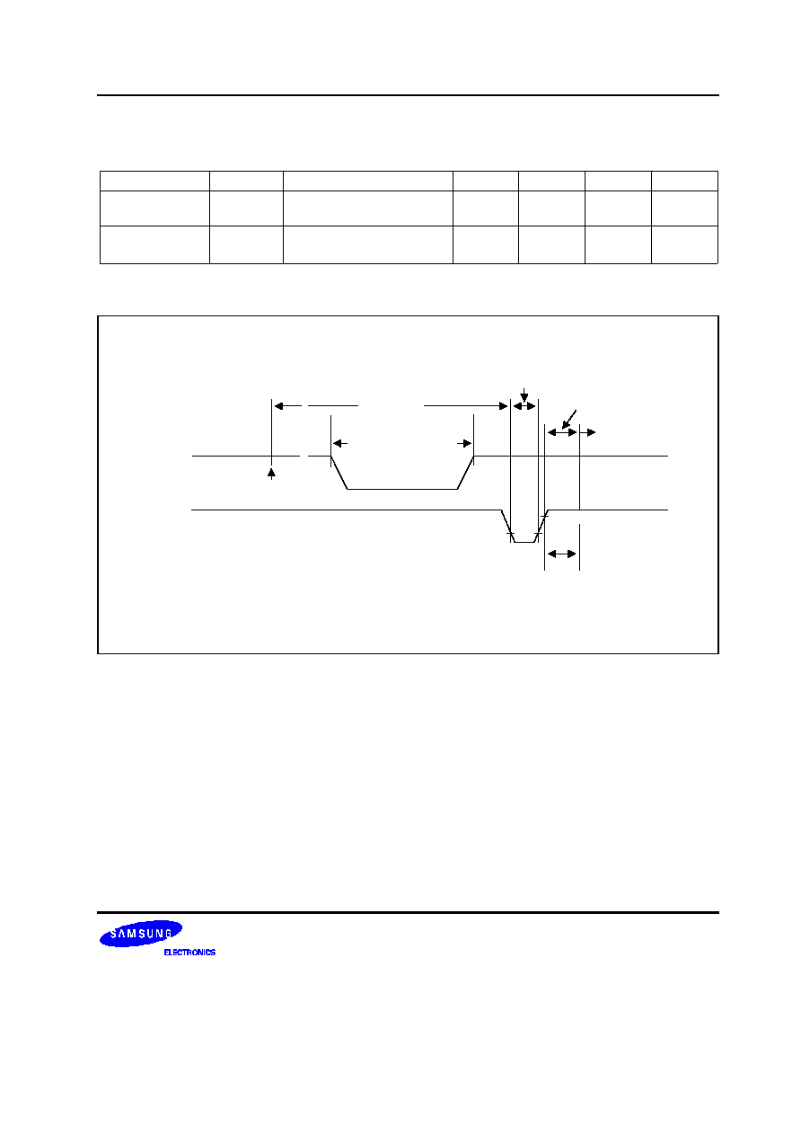
Figure 14-1. Input Timing Measurement Points
KS86C4302/C4304/P4304
ELECTRICAL DATA
14-5
Table 14-4. Oscillator Characteristics
(T
A
= - 40
�
C to + 85
�
C)
Oscillator
Clock Circuit
Test Condition
Min
Typ
Max
Unit
Main crystal or
ceramic
X
IN
C1
C2
X
OUT
V
DD
= 4.5 to 5.5 V
V
DD
= 3.0 to 4.5 V
1
1
�
�
16
8
MHz
External clock
X
IN
X
OUT
V
DD
= 4.5 to 5.5 V
V
DD
= 3.0 to 4.5 V
1
1
�
�
16
8
RC oscillator
X
IN
X
OUT
R
V
DD
= 5 V, R = 10 K
V
DD
= 3 V, R = 22 K
�
�
4
2
�
�
Table 14-5. Oscillation Stabilization Time
(T
A
= - 40
�
C to + 85
�
C, V
DD
= 3.0 V to 5.5 V)
Oscillator
Test Condition
Min
Typ
Max
Unit
Main crystal
f
OSC
> 1.0 MHz
�
�
20
ms
Main ceramic
Oscillation stabilization occurs when V
DD
is
equal to the minimum oscillator voltage range.
�
�
10
External clock
(main system)
X
IN
input high and low width (t
XH
, t
XL
)
25
�
500
ns
Oscillator
stabilization
t
WAIT
when released by a reset
(1)
�
2
16
/f
OSC
�
ms
wait time
t
WAIT
when released by an interrupt
(2)
�
�
�
NOTES:
1.
f
OSC
is the oscillator frequency.
2.
The duration of the oscillator stabilization wait time, t
WAIT
, when it is released by an interrupt is determined by the
settings
in the basic timer control register, BTCON.

ELECTRICAL DATA
KS86C4302/C4304/P4304
14-6
CPU Clock
16MHz
8MHz
4MHz
3MHz
2MHz
1MHz
1
2
3
4
5
6
7
2.7
5.5
Supply Voltage (V)
Figure 14-2. Operating Voltage Range
0.3 V
DD
A = 0.2 V
DD
B = 0.4 V
DD
C = 0.6 V
DD
D = 0.8 V
DD
V
OUT
A
0.7 V
DD
V
DD
V
SS
B
C
D
V
IN
Figure 14-3. Schmitt Trigger Input Characteristics Diagram
KS86C4302/C4304/P4304
ELECTRICAL DATA
14-7
Table 14-6. Data Retention Supply Voltage in Stop Mode
(T
A
= � 40
�
C to + 85
�
C, V
DD
= 3.0 V to 5.5 V)
Parameter
Symbol
Conditions
Min
Typ
Max
Unit
Data retention
supply voltage
V
DDDR
Stop mode
2.0
�
5.5
V
Data retention
supply current
I
DDDR
Stop mode; V
DDDR
= 2.0 V
�
0.1
5
uA
NOTE: Supply current does not include current drawn through internal pull-up resistors or external output current loads.
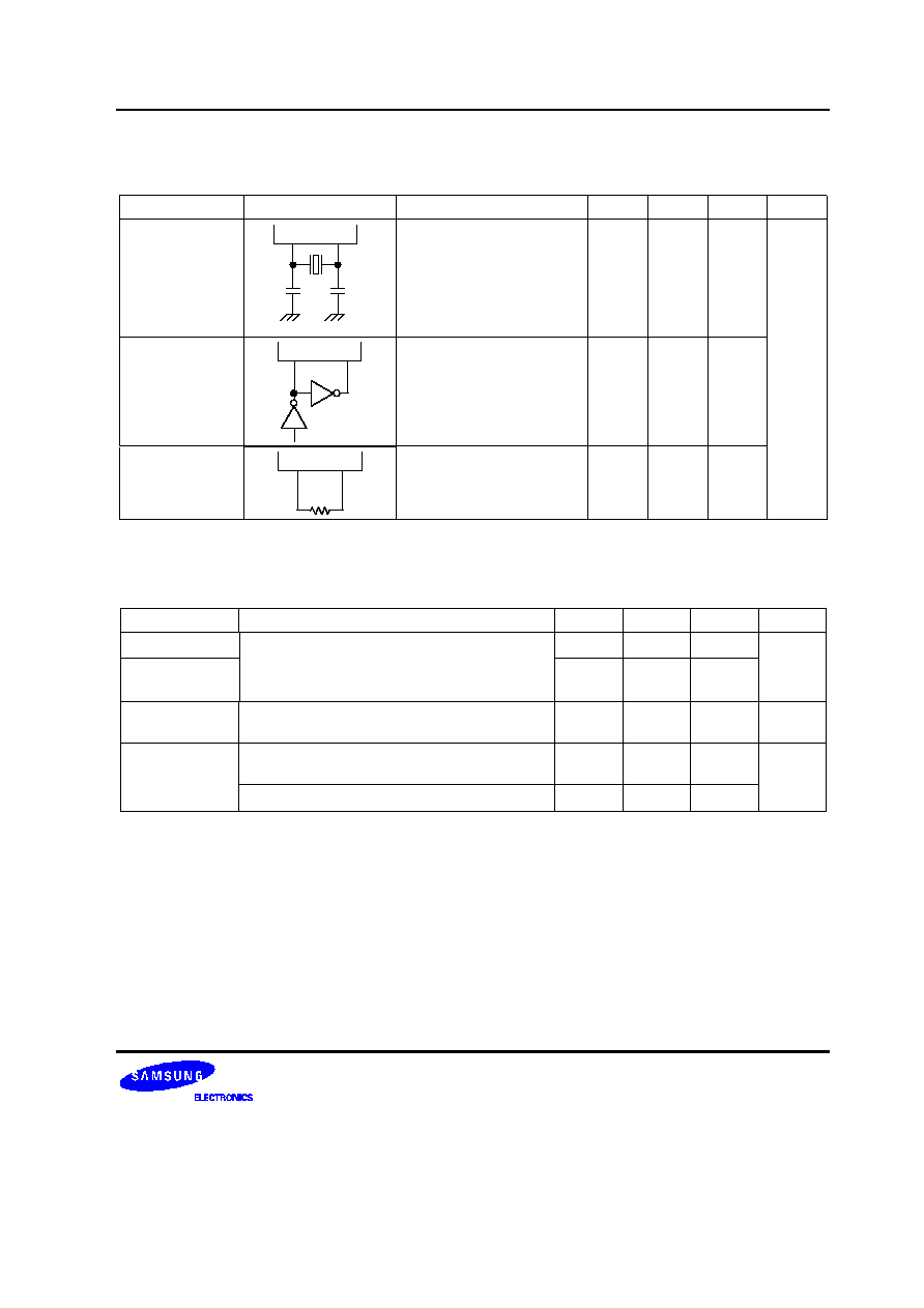
RESET
Data Retention Mode
~
~ ~
V
DDDR
Execution Of
Stop Instrction
V
DD
Normal
Operating
Mode
Oscillation
Stabilization Time
~
Stop Mode
Reset
Occurs
t
WAIT
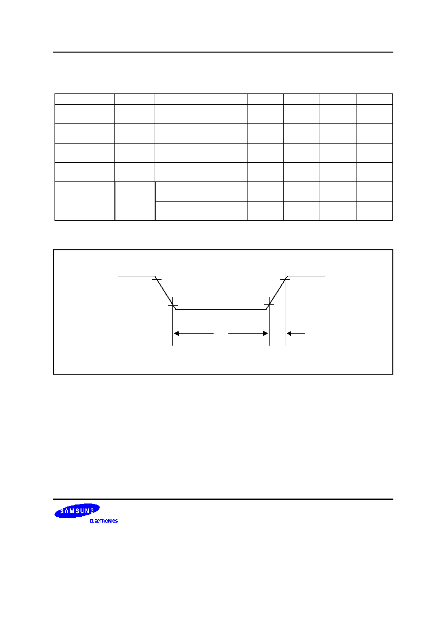
NOTE:
t
WAIT
is the same as 4096 x 16 x 1/fosc
0.8 V
DD
0.2 V
DD
Figure 14-4. Stop Mode Release Timing When Initiated by a
RESET
ELECTRICAL DATA
KS86C4302/C4304/P4304
14-8
Table 14-7. A/D Converter Electrical Characteristics
(T
A
= - 40
�
C to + 85
�
C, V
DD
= 3.0 V to 5.5 V, V
SS
= 0 V)
Parameter
Symbol
Test Conditions
Min
Typ
Max
Unit
Total accuracy
�
V
DD
= 5.12 V
CPU clock = 10 MHz
AV
REF
= 5.12 V
AV
SS
= 0 V
�
�
�
3
LSB
Integral linearity
error
ILE
�
�
�
�
2
Differential
linearity error
DLE
�
�
�
�
1
Offset error of
top
EOT
�
�
�
1
�
3
Offset error of
bottom
EOB
�
�
�
1
�
2
Conversion
time
(1)
t
CON
f
OSC
= 10 MHz
�
50x4/ f
OSC
�
�
s
Analog input
voltage
V
IAN
�
AV
SS
�
AV
REF
V
Analog input
impedance
R
AN
�
2
�
�
M
ADC reference
voltage
AV
REF
�
3.0
�
V
DD
V
ADC reference
ground
AV
SS
�
V
SS
�
V
SS
+ 0.3
V
Analog input
current
I
ADIN
AV
REF
= V
DD
= 5 V
�
�
10
�
A
Analog block
current
(2)
I
ADC
AV
REF
= V
DD
= 5 V
conversion time = 20
�
s
1
3
mA
AV
REF
= V
DD
= 3 V
conversion time = 20
�
s
0.5
1.5
mA
AV
REF
= V
DD
= 5 V
when power down mode
100
500
nA
NOTES:
1.
"Conversion time" is the time required from the moment a conversion operation starts until it ends.
2.
I
ADC
is operating current during A/D conversion.
KS86C4302/C4304/P4304
ELECTRICAL DATA
14-9
Table 14-8. LVD Circuit Characteristics
(T
A
= - 40
�
C to + 85
�
C, V
DD
= 3.0 V to 5.5V)
Parameter
Symbol
Conditions
Min
Typ
Max
Unit
Power-on reset
voltage high
V
DDH
3.0
5.5
V
Power-on reset
voltage low
V
DDL
0
2.6
3.0
V
Power supply
voltage rise time
t
r
10
(note)
us
Power supply
voltage off time
t
off
0.5
sec
Power-on reset
circuit
I
DDPR
V
DD
= 5 V
�
10 %
65
100
uA
consumption
current
V
DD
= 3 V
45
80
uA
NOTE: Oscillation stabilization time = 2
16
/fx (= 6.55 ms at fx = 10 MHz)
V
DD
V
DDH
V
DDL
t
OFF
t
R
Figure 14-5. LVD Reset Timing
ELECTRICAL DATA
KS86C4302/C4304/P4304
14-10
Table 14-9. Serial I/O Timing Characteristics
(T
A
= � 40
�
C to + 85
�
C, V
DD
= 3.0 V to 5.5 V)
Parameter
Symbol
Conditions
Min
Typ
Max
Unit
Cycle Time
t
CKY
External
source
1000
�
�
ns
Internal
source
1000
High, Low Width
t
KH
, t
KL
External
source
500
�
�
Internal
source
t
KCY
/2 � 50
SI Setup Time to
Low
t
SIK
External
source
250
�
�
Internal
source
250
SI Hold Time to
High
t
KSI
External
source
400
�
�
Internal
source
400
Output Delay for
to SO
t
KSO
External
source
�
�
300
Internal
source
250
NOTE:
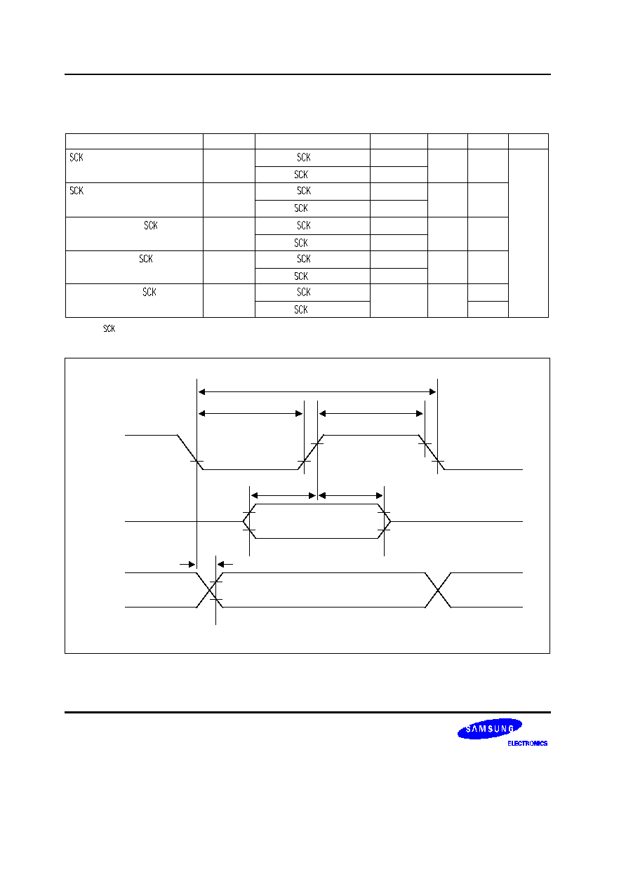
"
" means serial I/O clock frequency, "SI" means serial data input, and "SO" means serial data output.
Output Data
Input
SCK
t
KH
t
KCY
0.8 V
DD
0.2 V
DD
t
KSO
t
SIK
t
KSI
0.8 V
DD
0.2 V
DD
SI
SO
t
KL
Figure 14-6. Serial Data Transfer Timing
KS86C4302/C4304/P4304
ELECTRICAL DATA
14-11
0.0
5.0
1.0
2.0
3.0
4.0
fx = 16 MHz
V
DD
(V)
fx = 10 MHz
fx = 8 MHz
0.5
1.0
1.5
2.0
2.5
3.0
3.5
4.0
4.5
5.0
5.5
6.0
6.5
7.0
7.5
8.0
8.5
9.0
9.5
10.0
10.5
11.0
IDD1 (mA)
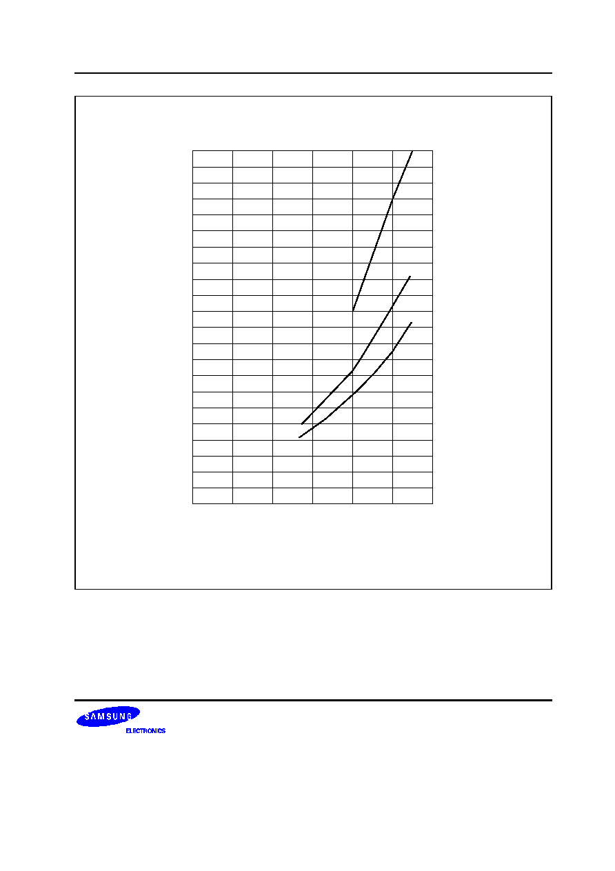
Figure 14-7. I
DD1
vs V
DD
ELECTRICAL DATA
KS86C4302/C4304/P4304
14-12
0.0
5.0
1.0
2.0
3.0
4.0
VOL (V)
5
10
15
20
25
30
35
40
45
50
55
60
65
70
75
80
IOL (mA)
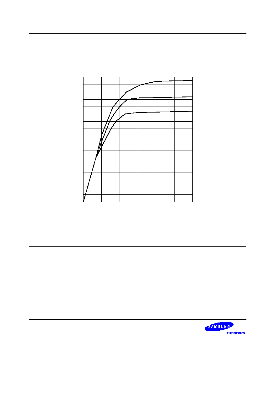
V
DD
= 4.5 V
V
DD
= 5.5 V
V
DD
= 5.0 V
Figure 14-8. I
OL
vs V
OL
KS86C4302/C4304/P4304
ELECTRICAL DATA
14-13
0.0
5.0
1.0
2.0
3.0
4.0
VOH (V)
-5
-10
-15
-20
-25
-30
-35
-40
-45
-50
-55
-60
-65
-70
-75
-80
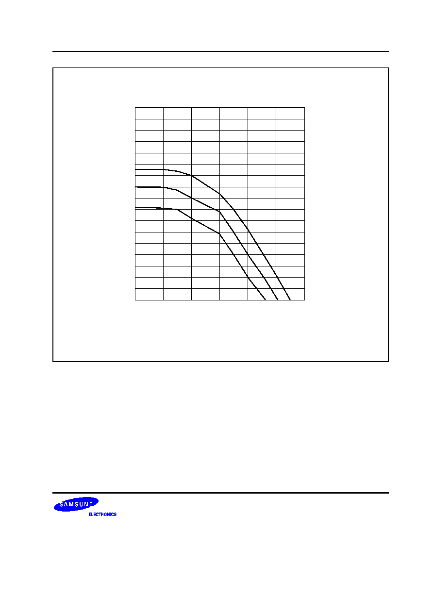
IOH (mA)
V
DD
= 5.5 V
V
DD
= 5.0 V
V
DD
= 4.5 V
Figure 14-9. I
OH
vs V
OH

ELECTRICAL DATA
KS86C4302/C4304/P4304
14-14
NOTES

KS86C4302/C4304/P4304
MECHANICAL DATA
15-1
15
MECHANICAL DATA
OVERVIEW
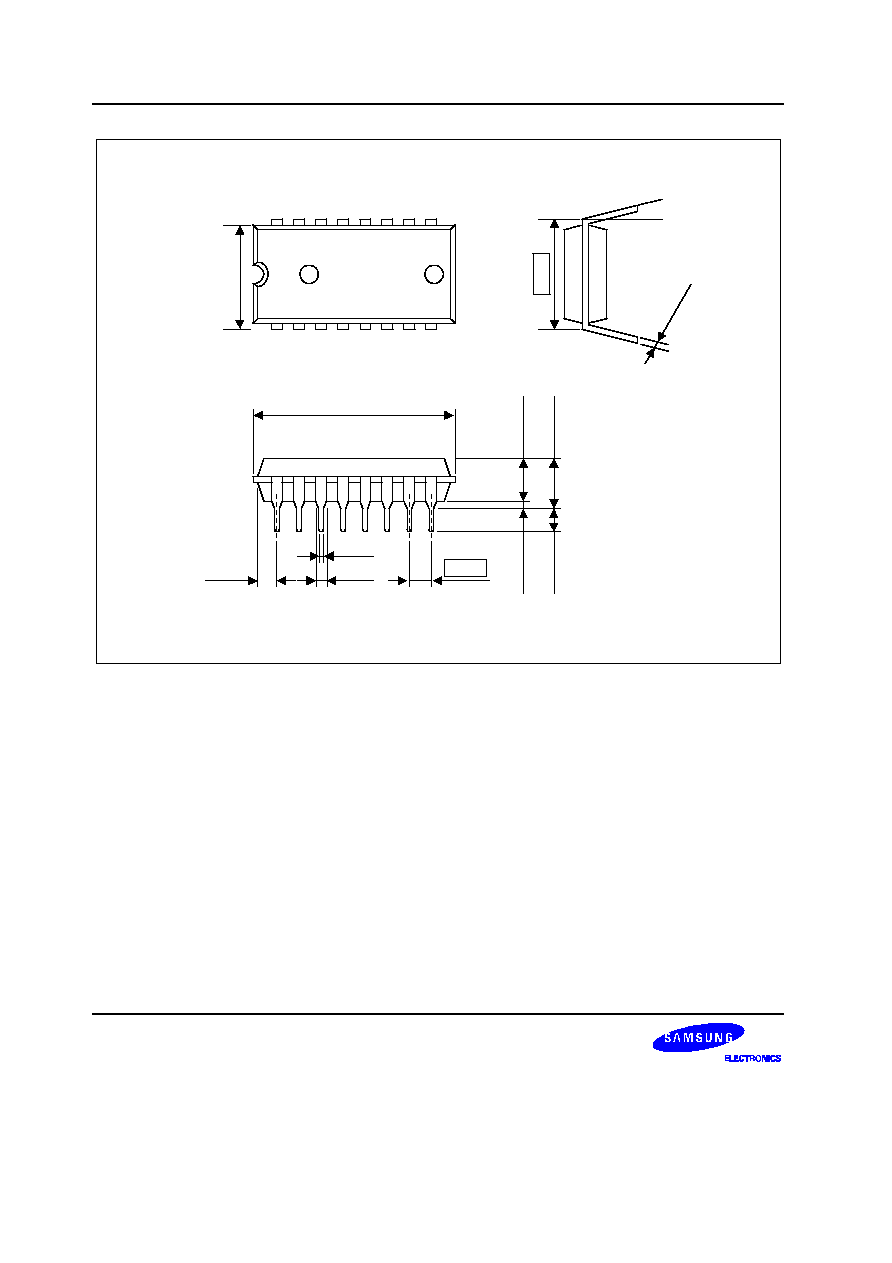
The KS86C4302/C4304 is available in a 20-pin SDIP package (Samsung: 20-DIP-300A), a 20-pin SOP package
(Samsung: 20-SOP-375), a 18-pin DIP package (Samsung: 18-DIP-300A). Package dimensions are shown in
Figure 15-1, 15-2, and 15-3.
NOTE : Dimensions are in millimeters.
26.80 MAX
26.40
� 0.20
(1.77)
20-DIP-300A
6.40
�
0
.20
#20
#1
0.46 �
0.10
1.52 �
0.10
#11
#10
0-15
0.25
+ 0.10- 0.05
7.62
2.54
0.51 MIN
3.30
� 0.30
3.25
�
0.20
5.08 MAX
Figure 15-1. 20-DIP-300A Package Dimensions

MECHANICAL DATA
KS86C4302/C4304/P4304
15-2
NOTE : Dimensions are in millimeters.
20-SOP-375
10.30
�
0
.30
#11
#20
#1
#10
13.14 MAX
12.74
� 0.20
(0.66)
0-8
0.203
+ 0.10
- 0.05
9.53
7.50
�
0.20
0.85
�
0.20
0.05 MIN
2.30
�
0.10
2.50 MAX
0.40
0.10 MAX
+ 0.10
- 0.05
1.27
Figure 15-2. 20-SOP-375 Package Dimensions

KS86C4302/C4304/P4304
MECHANICAL DATA
15-3
NOTE : Dimensions are in millimeters.
23.35 MAX
22.95
� 0.20
(1.32)
6.40
�
0
.20
#18
#1
#10
#9
0-15
0.25
+ 0.10- 0.05
7.62
2.54
0.51 MIN
3.30
� 0.30
3.25
�
0.20
5.08 MAX
18-DIP-300A
0.46 �
0.10
1.52 �
0.10
Figure 15-3. 18-DIP-300A Package Dimensions
MECHANICAL DATA
KS86C4302/C4304/P4304
15-4
19.80
(0.81)
6.40
#16
#1
#9
#8
0.25
7.62
2.54
1.50
0.46
0.38
3.25
3.30
5.08
Figure 15-4. 16-DIP-300A Package Dimensions
KS86C4302/C4304/P4304
KS86P4304 OTP
16-1
16
KS86P4304 OTP
OVERVIEW
The KS86P4304 single-chip CMOS microcontroller is the OTP (One Time Programmable)
version of the
KS86C4302/C4304 microcontroller. It has an on-chip OTP ROM instead of masked ROM. The EPROM is
accessed by serial data format.
The KS86P4304 is fully compatible with the KS86C4302/C4304, in function, in D.C. electrical characteristics, and
in pin configuration. Because of its simple programming requirements, the KS86P4304 is ideal for use as an
evaluation chip for the KS86C4302/C4304.
V
SS
/V
SS
X
IN
X
OUT
V
PP
/TEST
P0.2/T0CK/INT0
P0.1/PWM
RESET/RESET
P0.0/BUZ
P2.0/SCK
P2.2
NOTE:
The bolds indicate an OTP pin name.
KS86P4304
(TOP VIEW)
V
DD/
V
DD
P0.3/INT1/SCLK
P1.0/ADC0/SDAT
P1.1/ADC1/SI
P1.2/ADC2/SO
P1.3/ADC3/SCK
P1.4/ADC4/CLO
AV
REF
P2.1/SO
P2.3
20
19
18
17
16
15
14
13
12
11
1
2
3
4
5
6
7
8
9
10
Figure 16-1. Pin Assignment Diagram (20-Pin DIP Package)
KS86P4304 OTP
KS86C4302/C4304/P4304
16-2
KS86P4304
(TOP VIEW)
V
DD/
V
DD
P0.3/INT1/SCLK
P1.0/ADC0/SDAT
P1.1/ADC1/SI
P1.2/ADC2/SO
P1.3/ADC3/SCK
P1.4/ADC4/CLO
AV
REF
P2.1/SO
P2.3
20
19
18
17
16
15
14
13
12
11
V
SS
/V
SS
X
IN
X
OUT
V
PP
/TEST
P0.2/T0CK/INT0
P0.1/PWM
RESET/RESET
P0.0/BUZ
P2.0/SCK
P2.2
1
2
3
4
5
6
7
8
9
10
NOTE:
The bolds indicate an OTP pin name.
Figure 16-2. Pin Assignment Diagram (20-Pin SOP Package)
KS86C4302/C4304/P4304
KS86P4304 OTP
16-3
KS86P4304
(TOP VIEW)
V
DD/
V
DD
P0.3/INT1/SCLK
P1.0/ADC0/SDAT
P1.1/ADC1/SI
P1.2/ADC2/SO
P1.3/ADC3/SCK
P1.4/ADC4/CLO
AV
REF
P2.1/SO
18
17
16
15
14
13
12
11
10
V
SS
/V
SS
X
IN
X
OUT
V
PP
/TEST
P0.2/T0CK/INT0
P0.1/PWM
RESET/RESET
P0.0/BUZ
P2.0/SCK
1
2
3
4
5
6
7
8
9
NOTE:
The bolds indicate an OTP pin name.
Figure 16-3. Pin Assignment Diagram (18-Pin DIP Package)
KS86P4304 OTP
KS86C4302/C4304/P4304
16-4
KS86P4304
(TOP VIEW)
V
DD/
V
DD
P0.3/INT1/SCLK
P1.0/ADC0/SDAT
P1.1/ADC1/SI
P1.2/ADC2/SO
P1.3/ADC3/SCK
P1.4/ADC4/CLO
AV
REF
16
15
14
13
12
11
10
9
V
SS
/V
SS
X
IN
X
OUT
V
PP
/TEST
P0.2/T0CK/INT0
P0.1/PWM
RESET/RESET
P0.0/BUZ
1
2
3
4
5
6
7
8
NOTE:
The bolds indicate an OTP pin name.
Figure 16-4. Pin Assingment Diagram (16-Pin DIP Package)
KS86C4302/C4304/P4304
KS86P4304 OTP
16-5
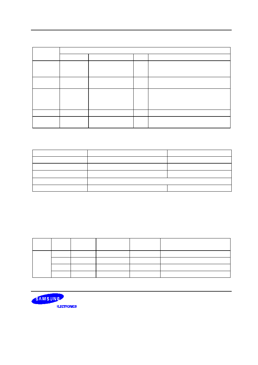
Table 16-1. Descriptions of Pins Used to Read/Write the EPROM
Main Chip
During Programming
Pin Name
Pin Name
Pin No.
I/O
Function
P0.3
SDAT
18 (20-pin)
16 (18-pin)
I/O
Serial data pin (output when reading, Input
when writing) Input and push-pull output
port can be assigned
P0.2
SCLK
19 (20-pin)
17 (18-pin)
I
Serial clock pin (input only pin)
TEST
V
PP
(TEST)
4
I
Power supply pin for EPROM cell writing (indicates
that OTP enters into the writing mode). When 12.5
V is applied, OTP is in writing mode and when 5 V
is applied, OTP is in reading mode. (Option)
RESET
RESET
7
I
Chip Initialization
V
DD
/V
SS
V
DD
/V
SS
20 (20-pin), 18 (18-pin)
1 (20-pin), 1 (18-pin)
I
Logic power supply pin.
NOTE:
( ) means the SOP OTP pin number.
Table 16-2. Comparison of KS86P4304 and KS86C4302/C4304 Features
Characteristic
KS86P4304
KS86C4302/C4304
Program Memory
4 Kbyte EPROM
2K/4K byte mask ROM
Operating Voltage (V
DD
)
3.0 V to 5.5 V
3.0 V to 5.5 V
OTP Programming Mode
V
DD
= 5 V, V
PP
(TEST) = 12.5 V
Pin Configuration
20 DIP/20 SOP/18 DIP
EPROM Programmability
User Program 1 time
Programmed at the factory
OPERATING MODE CHARACTERISTICS
When 12.5 V is supplied to the VPP (TEST) pin of the KS86P4304, the EPROM programming mode is entered.
The operating mode (read, write, or read protection) is selected according to the input signals to the pins listed in
Table 16-3 below.
Table 16-3. Operating Mode Selection Criteria
VDD
VPP
(TEST)
REG/
MEM
ADDRESS
(A15-A0)
R/W
MODE
5 V
5 V
0
0000H
1
EPROM read
12.5 V
0
0000H
0
EPROM program
12.5 V
0
0000H
1
EPROM verify
12.5 V
1
0E3FH
0
EPROM read protection
NOTE: "0" means Low level; "1" means High level.

KS86P4304 OTP
KS86C4302/C4304/P4304
16-6
NOTES