
S3C80F7/C80F9/C80G7/C80G9 (KS88C01524/C01532/C01624/C01632)
PRODUCT OVERVIEW
1-1
1
PRODUCT OVERVIEW
S3C8-SERIES MICROCONTROLLERS
Samsung's S3C8 series of 8-bit single-chip CMOS microcontrollers offers a fast and efficient CPU, a wide range
of integrated peripherals, and various mask-programmable ROM sizes. Important CPU features include:
-- Efficient register-oriented architecture
-- Selectable CPU clock sources
-- Idle and Stop power-down mode release by interrupt
-- Built-in basic timer with watchdog function
A sophisticated interrupt structure recognizes up to eight interrupt levels. Each level can have one or more
interrupt sources and vectors. Fast interrupt processing (within a minimum six CPU clocks) can be assigned to
specific interrupt levels.
S3C80F7/C80F9/C80G7/C80G9 Microcontroller
The S3C80F7/C80F9/C80G7/C80G9 single-chip CMOS microcontroller is fabricated using a highly advanced
CMOS process and is based on Samsung's newest CPU architecture.
The S3C80F9/C80G9 is the microcontroller which has 32-Kbyte mask-programmable ROM and S3C80F7/C80G7
is the microcontroller which has 24-Kbyte mask-programmable ROM.
The S3P80F9/P80G9 is the microcontroller which has 32-Kbyte one-time-programmable EPROM and
S3P80F7/P80G7 is the microcontroller which has 24-Kbyte one-time-programmable EPROM.
Using a proven modular design approach, Samsung engineers developed S3C80F7/C80F9/C80G7/C80G9 by
integrating the following peripheral modules with the powerful SAM87 RC core:
-- Internal LVD circuit and 16 bit-programmable pins for external interrupts.
-- One 8-bit basic timer for oscillation stabilization and watchdog function (system reset).
-- One 8-bit timer/counter and one 16-bit timer/counter with selectable operating modes.
-- One 8-bit counter with auto-reload function and one-shot or repeat control.
The S3C80F7/C80F9/C80G7/C80G9 is a versatile general-purpose microcontroller which is especially suitable
for use as remote transmitter controller. It is currently available in a 32-pin SOP, 42-pin SDIP and 44-pin QFP
package.

PRODUCT OVERVIEW S3C80F7/C80F9/C80G7/C80G9 (KS88C01524/C01532/C01624/C01632)
1-2
FEATURES
CPU
∑
SAM87RC CPU core
Memory
∑
32-Kbyte internal ROM (S3C80F9/C80G9)
: 0000H≠7FFFH
∑
24-Kbyte internal ROM (S3C80F7/C80G7)
: 0000H≠5FFFH
∑
Data memory: 272-byte RAM (318 register)
Instruction Set
∑
78 instructions
∑
IDLE and STOP instructions added for power-
down modes
Instruction Execution Time
∑
500 ns at 8-MHz f
OSC
(minimum)
Interrupts
∑
22 interrupt sources with 16 vector and 7 level.
I/O Ports
∑
Three 8-bit I/O ports (P0≠P2), one 8-bit output
port(P4) and 6-bit port (P3) for a total of 38 bit-
programmable pins.(44-QFP)
∑
Three 8-bit I/O ports (P0≠P2), one 8-bit output
port(P4) and 4-bit port (P3) for a total of 36 bit-
programmable pins.(42-SDIP)
∑
Three 8-bit I/O ports (P0≠P2) and one 2-bit I/O
port (P3) for a total of 26-bit programmable pins.
(32-SOP)
Timers and Timer/Counters
∑
One programmable 8-bit basic timer (BT) for
oscillation stabilization control or watchdog timer
(software reset) function
∑
One 8-bit timer/counter (Timer 0) with three
operating modes; Interval mode, Capture and
PWM mode.
∑
One 16-bit timer/counter (Timer1) with two
operating modes; Interval mode and Capture.
Carrier Frequency Generator
∑
One 8-bit counter with auto-reload function and
one-shot or repeat control (Counter A)
Back-up mode
∑
When V
DD
is lower than V
LVD
, the chip enters
Back-up mode to block oscillation and reduce
the current consumption.
In S3C80G7/C80G9, this function is disabled
when operating state is "STOP mode".
∑
When
RESET
pin is lower than Input Low
Voltage (V
IL
), the chip enters Back-up mode to
block oscillation and reduce the current
consumption.
Low Voltage Detect Circuit
∑
Low voltage detect to get into Back-up mode.
∑
Low level detect voltage
-
S3C80F7/C80F9: 2.20 V (Typ)
±
200mV
-
S3C80G7/C80G9: 1.90 V (Typ)
±
200mV
Operating Temperature Range
∑
≠40
∞
C to + 85
∞
C
Operating Voltage Range
∑
1.7V to 5.0V at 4 MHz f
OSC
(S3C80G7/C80G9)
∑
2.0V to 5.0V at 8 MHz f
OSC
(S3C80F7/C80F9)
Package Type
∑
44-pin QFP-1010B
∑
42-pin SDIP
∑
32-pin SOP

S3C80F7/C80F9/C80G7/C80G9 (KS88C01524/C01532/C01624/C01632)
PRODUCT OVERVIEW
1-3
BLOCK DIAGRAM
Port 0
P0.0-0.3 (INT0-INT3)
P0.4-P0.7 (INT4)
I/O Port and Interrupt
Control
32K-Bytes
ROM
317-Bytes
Register
File
SAM87RC
CPU
Port 1
P2.0-2.3 (INT5-INT8)
Port 4
P4.0-4.7
LVD
P1.0-P1.7
TEST
RESET
MAIN
OSC
8-Bit
Basic
Timer
8-Bit
Timer/
Counter
16-Bit
Timer/
Counter
V
DD
Carrier
Registor
(Counter A)
X
OUT
X
IN
Port 3
Port 2
P2.4-2.7 (INT9)
P3.0-T0PWM/
T0CAP/(T1CAP)
P3.1-REM/(T0CK)
P3.2/(T0CK)
P3.3/(T1CAP)
P3.4-3.5
Figure 1-1. Block Diagram

PRODUCT OVERVIEW
S3C80F7/C80F9/C80G7/C80G9 (KS88C01524/C01532/C01624/C01632)
1-4
PIN ASSIGNMENTS
P4.2
P4.1
P4.0
P2.0/INT5
P2.1/INT6
P2.2/INT7
P2.3/INT8
P2.4/INT9
P3.0/T0PWM/T0CAP/SDAT
R3.1/REM/SCLK
V
DD
V
SS
X
OUT
X
IN
TEST
P2.5/INT9
P2.6/INT9
RESET
P2.7/INT9
P1.0
P3.2/T0CK
1
2
3
4
5
6
7
8
9
10
11
12
13
14
15
16
17
18
19
20
21
P4.3
P0.7/INT4
P0.6/INT4
P0.5/INT4
P0.4/INT4
P0.3/INT3
P0.2/INT2
P0.1/INT1
P0.0/INT0
P4.4
P4.5
P4.6
P1.7
P1.6
P1.5
P1.4
P1.3
P1.2
P1.1
P4.7
P3.3/T1CAP
42
41
40
39
38
37
36
35
34
33
32
31
30
29
28
27
26
25
24
23
22
S3C80F7/C80F9
/C80G7/C80G9
(Top View)
42-SDIP
Figure 1-2. Pin Assignment Diagram (42-Pin SDIP Package)
S3C80F7/C80F9/C80G7/C80G9 (KS88C01524/C01532/C01624/C01632)
PRODUCT OVERVIEW
1-5
P0.3/INT3
P0.2/INT2
P0.1/INT1
P0.0/INT0
P4.4
P4.5
P4.6
P1.7
P1.6
P1.5
P1.4
P0.4/INT4
P0.5/INT4
P0.6/INT4
P0.7/INT4
P4.3
P4.2
P4.1
P4.0
P2.0/INT5
P2.1/INT6
P2.2/INT7
S3C80F7/C80F9
/C80G7/C80G9
(Top View)
(44-QFP)
34
35
36
37
38
39
40
41
42
43
44
33
32
31
30
29
28
27
26
25
24
23
P1.3
P1.2
P1.1
P4.7
P3.3/T1CAP
P3.2/T0CK
P1.0
P2.7/INT9
P3.5
P3.4
RESET
22
21
20
19
18
17
16
15
14
13
12
P2.3/INT8
P2.4/INT9
P3.0/T0PWM/T0CAP/
SDAT
P3.1/REM/
SCLK
V
DD
V
SS
X
OUT
X
IN
TEST
P2.5/INT9
P2.6/INT9
1
2
3
4
5
6
7
8
9
10
11
Figure 1-3. Pin Assignment Diagram (44-Pin QFP Package)
PRODUCT OVERVIEW
S3C80F7/C80F9/C80G7/C80G9 (KS88C01524/C01532/C01624/C01632)
1-6
V
SS
X
IN
X
OUT
TEST
P2.5/INT9
P2.6/INT9
RESET
P2.7/INT9
P1.0
P1.1
P1.2
P1.3
P1.4
P1.5
P1.6
P1.7
S3C80F7/C80F9
/C80G7/C80G9
(Top View)
32-SOP
1
2
3
4
5
6
7
8
9
10
11
12
13
14
15
16
V
DD
P3.1/REM/T0CK/SCLK
P3.0/T0PWM/T0CAP/T1CAP/SDAT
P2.4/INT9
P2.3/INT8
P2.2/INT7
P2.1/INT6
P2.0/INT5
P0.7/INT4
P0.6/INT4
P0.5/INT4
P0.4/INT4
P0.3/INT3
P0.2/INT2
P0.1/INT1
P0.0/INT0
32
31
30
29
28
27
26
25
24
23
22
21
20
19
18
17
Figure 1-4. Pin Assignment Diagram (32-Pin SOP Package)
S3C80F7/C80F9/C80G7/C80G9 (KS88C01524/C01532/C01624/C01632)
PRODUCT OVERVIEW
1-7
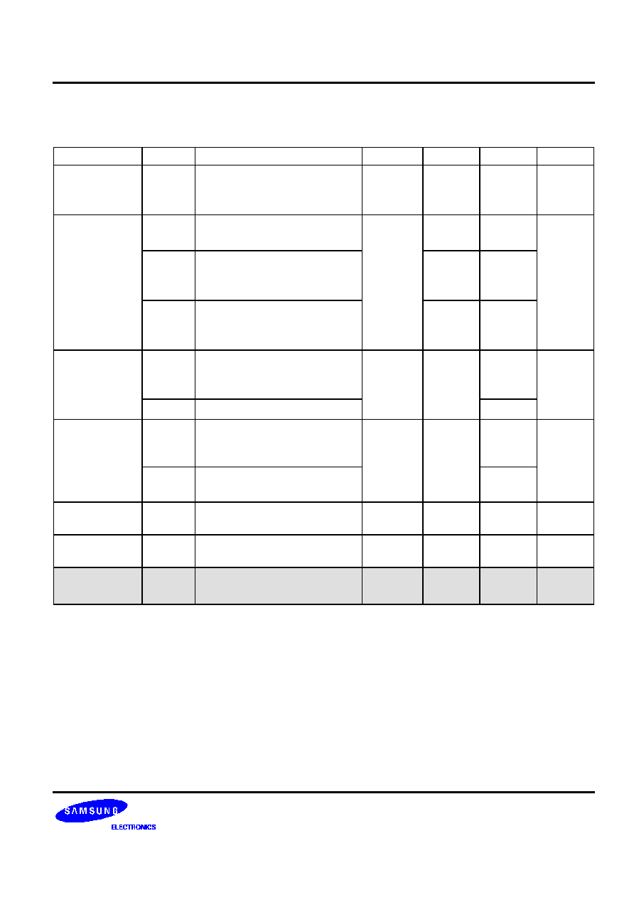
Table 1-1. Pin Descriptions of 44-QFP and 42-SDIP
Pin
Names
Pin
Type
Pin Description
Circuit
Type
42 Pin
No.
44 Pin
No.
Shared
Functions
P0.0≠P0.7
I/O
I/O port with bit-programmable pins.
Configurable to input or push-pull output
mode. Pull-up resistors can be assigned
by software. Pins can be assigned
individually as external interrupt inputs
with noise filters, interrupt enable/
disable, and interrupt pending control.
SED & R circuit built in P0 for STOP
releasing.
1
34≠41
30≠37
Ext. INT
(INT0 - 4)
P1.0≠P1.7
I/O
I/O port with bit-programmable pins.
Configurable to input mode or output
mode. Pin circuits are either push-pull or
n-channel open-drain type.
2
20
24≠30
16
20≠26
≠
P2.0≠P2.3
P2.4≠P2.7
I/O
I/O port with bit-programmable pins.
Configurable to input or push-pull output
mode. Pull-up resistors can be assigned
by software. Pins can be assigned
individually as external interrupt inputs
with noise filters, interrupt enable/
disable, and interrupt pending control.
SED & R circuit built in P2 for STOP
releasing.
1
4≠8,
16, 17
19
42≠44
1,2,
10,11,
15
Ext. INT
(INT5≠9)
P3.0
P3.1
I/O
2-bit I/O port with bit-programmable pins.
Configurable to input mode, push-pull
output mode, or n-channel open-drain
output mode. Input mode with pull-up
resistors can be assigned by software.
The two port 3 pins have high current
drive capability
3
4
9≠10
3≠4
T0PWM/ T0CAP
REM
P3.2≠P3.3
I
C-MOS Input port with pull-up resistors
5
21
22
17
18
(T0CK)
(T1CAP)
P3.4≠P3.5
O
Open drain output port for high current
drive
6
None
13≠14
≠
P4.0≠P4.7
O
8- bit-programmable output pins.
Configurable to open drain output port or
push-pull output port.
7
1≠3
42,23
31-33
41≠38
27≠29
19
≠
X
IN
, X
OUT
≠
System clock input and output pins
≠
13,14
7,8
≠
RESET
I
System reset signal input pin and back-
up mode input.
8
18
12
≠
TEST
I
Test signal input pin (for factory use only;
must be connected to V
SS
.)
≠
15
9
≠
V
DD
≠
Power supply input pin
≠
11
5
≠
V
SS
≠
Ground pin
≠
12
6
≠
PRODUCT OVERVIEW
S3C80F7/C80F9/C80G7/C80G9 (KS88C01524/C01532/C01624/C01632)
1-8
Table 1-2. Pin Descriptions of 32-SOP
Pin
Names
Pin
Type
Pin Description
Circuit
Type
32 Pin
No.
Shared
Functions
P0.0≠P0.7
I/O
I/O port with bit-programmable pins.
Configurable to input or push-pull output
mode. Pull-up resistors are assignable by
software. Pins can be assigned individually as
external interrupt inputs with noise filters,
interrupt enable/ disable, and interrupt pending
control. SED & R circuit built in P0 for STOP
releasing.
1
17≠24
Ext. INT
P1.0≠P1.7
I/O
I/O port with bit-programmable pins.
Configurable to input mode or output mode.
Pin circuits are either push-pull or n-channel
open-drain type.
2
9≠16
≠
P2.0≠P2.3
P2.4≠P2.7
I/O
I/O port with bit-programmable pins.
Configurable to input or push-pull output
mode. Pull-up resistors can be assigned by
software. Pins can be assigned individually as
external interrupt inputs with noise filters,
interrupt enable/disable, and interrupt pending
control. SED & R circuit built in P2 for STOP
releasing.
1
25≠28
29,5, 6,8
Ext. INT
P3.0
P3.1
I/O
2-bit I/O port with bit-programmable pins.
Configurable to input mode, push-pull output
mode, or n-channel open-drain output mode.
Input mode with pull-up resistors can be
assigned by software. The two port 3 pins
have high current drive capability.
3
4
30,31
T0PWM/
T0CAP/T1CAP
REM/T0CK
X
IN
, X
OUT
≠
System clock input and output pins
≠
2,3
≠
RESET
I
System reset signal input pin and back-up
mode input.
8
7
≠
TEST
I
Test signal input pin (for factory use only;
must be connected to V
SS
).
≠
4
≠
V
DD
≠
Power supply input pin
≠
32
≠
V
SS
≠
Ground pin
≠
1
≠
S3C80F7/C80F9/C80G7/C80G9 (KS88C01524/C01532/C01624/C01632)
PRODUCT OVERVIEW
1-9
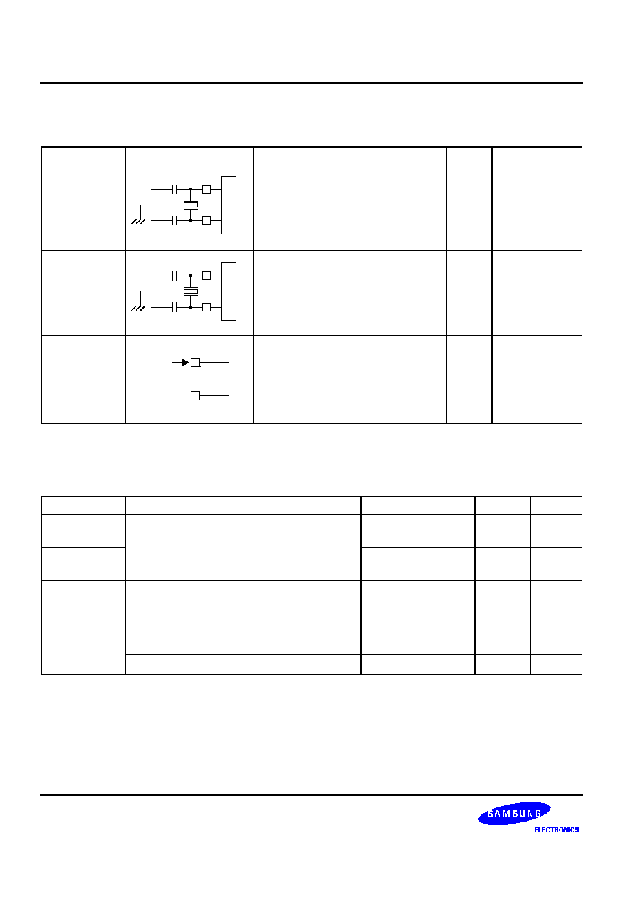
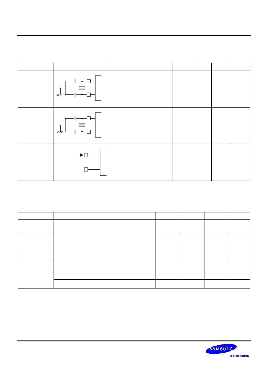
PIN CIRCUITS
V
DD
Pull-up
Resistor
V
DD
V
SS
Noise
Filter
Input/
Output
Stop release
Pull-up
Enable
Data
Output
Disable
External
Interrupt
Stop
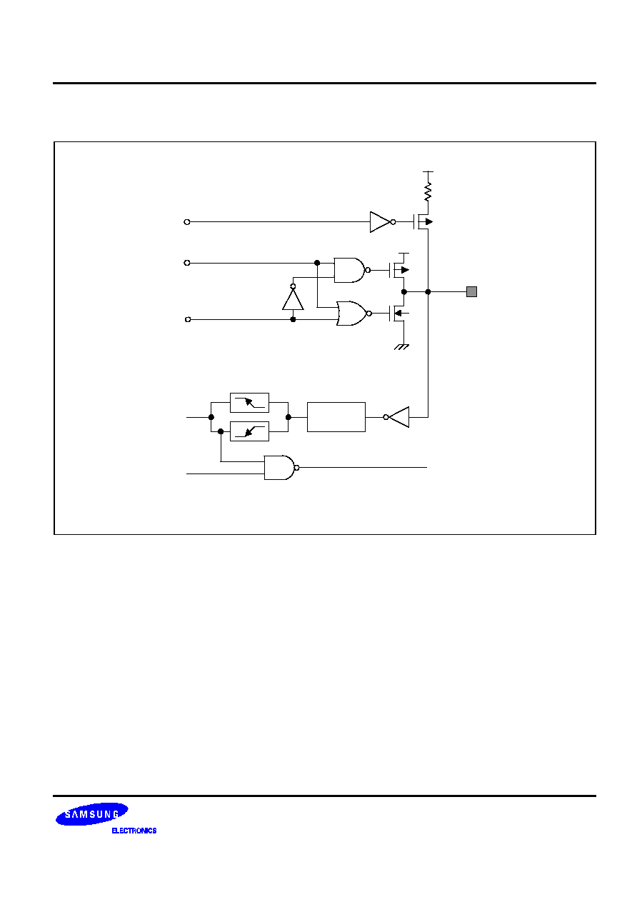
Figure 1-5. Pin Circuit Type 1 (Port 0 and Port2)
PRODUCT OVERVIEW
S3C80F7/C80F9/C80G7/C80G9 (KS88C01524/C01532/C01624/C01632)
1-10
PIN CIRCUITS (Continued)
V
DD
Pull-up
Resistor
V
DD
V
SS
Noise
Filter
Input/
Output
Pull-up
Enable
Data
Output Disable
Normal
Input
Open-Drain
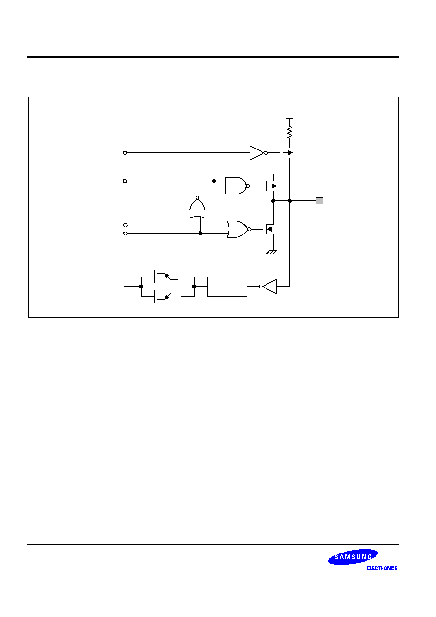
Figure 1-6. Pin Circuit Type 2 (Port 1)

S3C80F7/C80F9/C80G7/C80G9 (KS88C01524/C01532/C01624/C01632)
PRODUCT OVERVIEW
1-11
PIN CIRCUITS (Continued)
V
DD
Pull-up
Enable
V
DD
P3.0/T0PWM
T0CAP/(T1CAP)
Pull-up
Resistor
Open-Drain
Port 3.0 Data
V
SS
P3.0 Input
M
U
X
P3CON.2
Data
Output Disable
T0CAP/(T1CAP)
T0_PWM
Noise filter
M
U
X
P3CON.2,6,7
Figure 1-7. Pin Circuit Type 3 (P3.0)

PRODUCT OVERVIEW
S3C80F7/C80F9/C80G7/C80G9 (KS88C01524/C01532/C01624/C01632)
1-12
PIN CIRCUITS (Continued)
V
DD
Pull-up
Enable
V
DD
P3.1/REM/(T0CK)
Pull-up
Resistor
Open-Drain
Port 3.1 Data
V
SS
P3.1 Input
M
U
X
P3CON.5
Data
Output
Disable
T0CK
CAOF(CACON.0)
Carrier On/Off (P3.7)
Noise filter
M
U
X
P3CON.5,6,7
Figure 1-8. Pin Circuit Type 4 (P3.1) Circuit
V
DD
Pull-up
Resistor
Input
T0CK : P3.2
T1CAP: P3.3
M
U
X
Figure 1-9. Pin Circuit Type 5 (P3.2, P3.3)
S3C80F7/C80F9/C80G7/C80G9 (KS88C01524/C01532/C01624/C01632)
PRODUCT OVERVIEW
1-13
PIN CIRCUITS (Continued)
Data
Output
V
SS
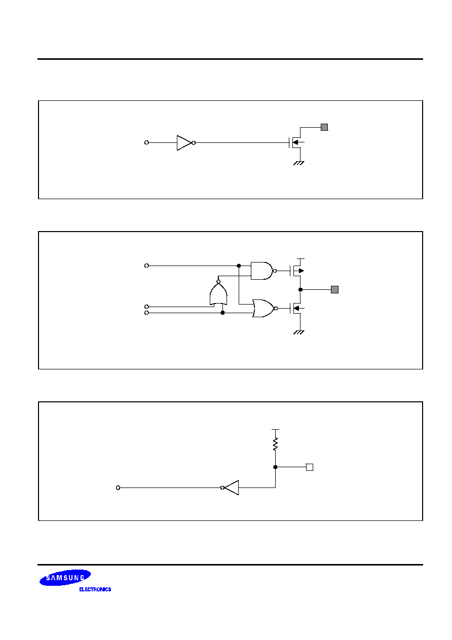
Figure 1-10. Pin Circuit type 6 (P3.4, P3.5)
V
DD
V
SS
Output
Data
Open-Drain
Output Disable
Figure 1-11. Pin Circuit type 7 (Port 4)
V
DD
Pull-up
Resistor
RESET
Figure 1-12. Pin Circuit type 8 (
RESET
)

S3C80F7/C80F9/C80G7/C80G9 (KS88C01524/C01532/C01624/C01632)
ELECTRICAL DATA
14-1
14
ELECTRICAL DATA 1 (S3C80F7/C80F9)
OVERVIEW
In this section, S3C80F7/C80F9 electrical characteristics are presented in tables and graphs. The information is
arranged in the following order:
-- Absolute maximum ratings
-- D.C. electrical characteristics
-- Data retention supply voltage in Stop mode
-- Stop mode release timing when initiated by an external interrupt
-- Stop mode release timing when initiated by a Reset
-- I/O capacitance
-- A.C. electrical characteristics
-- Input timing for external interrupts
-- Input timing for
RESET
-- Oscillation characteristics
-- Oscillation stabilization time

ELECTRICAL DATA
S3C80F7/C80F9/C80G7/C80G9 (KS88C01524/C01532/C01624/C01632)
14-2
Table 14-1. Absolute Maximum Ratings
(T
A
= 25
∞
C)
Parameter
Symbol
Conditions
Rating
Unit
Supply voltage
V
DD
≠
≠ 0.3 to + 6.5
V
Input voltage
V
IN
≠
≠ 0.3 to
V
DD
+ 0.3
V
Output voltage
V
O
All output pins
≠ 0.3 to V
DD
+ 0.3
V
Output current High
I
OH
One I/O pin active
≠ 18
mA
All I/O pins active
≠ 60
Output current Low
I
OL
One I/O pin active
+ 30
mA
Total pin current for ports 0, 1, and 2
+ 100
Total pin current for port 3
+ 40
Operating
temperature
T
A
≠
≠ 40 to + 85
∞
C
Storage temperature
T
STG
≠
≠ 65 to + 150
∞
C
Table 14-2. D.C. Electrical Characteristics
(T
A
= ≠ 40
∞
C to + 85
∞
C, V
DD
= 2.0 V to 5.0 V)
Parameter
Symbol
Conditions
Min
Typ
Max
Unit
Operating Voltage
V
DD
F
OSC
= 8 MHz
(Instruction clock = 2 MHz)
2.0
≠
5.0
V
Input High
voltage
V
IH1
All input pins except V
IH2
and V
IH3
0.8 V
DD
≠
V
DD
V
V
IH2
RESET
0.85 V
DD
V
DD
V
IH3
XIN
V
DD
≠ 0.3
V
DD
Input Low voltage
V
IL1
All input pins except V
IL2
and V
IL3
0
≠
0.2 V
DD
V
V
IL2
RESET
0.2 V
DD
V
IL3
XIN
0.3
Output High
voltage
V
OH1
V
DD
= 2.4 V I
OH
= ≠ 6 mA
Port 3.1 only, TA = 25
∞
C
V
DD
≠ 0.7
V
V
OH2
V
DD
= 2.4 V, I
OH
= ≠ 2.2mA
P3.0, P2.0≠2.3
T
A
= 25
∞
C
V
DD
≠
0.7
S3C80F7/C80F9/C80G7/C80G9 (KS88C01524/C01532/C01624/C01632)
ELECTRICAL DATA
14-3
Table 14-2. D.C. Electrical Characteristics (Continued)
(T
A
= ≠ 40
∞
C to + 85
∞
C, V
DD
= 2.0 V to 5.0 V)
Parameter
Symbol
Conditions
Min
Typ
Max
Unit
Output High
voltage
V
OH3
V
DD
= 2.4 V,I
OH
= ≠ 1 mA
Port0, Port1, P2.4-2.7 and Port4
T
A
= 25
∞
C
V
DD
≠
1.0
≠
≠
V
Output Low
voltage
V
OL1
V
DD
= 2.4 V, I
OL
= 12 mA, port
3.1 only, T
A
= 25
∞
C
≠
0.4
0.5
V
V
OL2
V
DD
= 2.4 V, I
OL
= 5 mA
P3.0, P3.4-3.5, P2.0-2.3
T
A
= 25
∞
C
0.4
0.5
V
OL3
I
OL
= 2mA
Port 0, Port1, P2.4-2.7 and Port4
T
A
= 25
∞
C
0.4
1
Input High
leakage current
I
LIH1
V
IN
= V
DD
All input pins except X
IN
and
X
OUT
≠
≠
1
µA
I
LIH2
V
IN
= V
DD
, X
IN
and X
OUT
20
Input Low
leakage current
I
LIL1
V
IN
= 0 V
All input pins except X
IN
, X
OUT
,
and
RESET
≠
≠
≠ 1
µA
I
LIL2
V
IN
= 0 V
X
IN
and X
OUT
≠ 20
Output High
leakage current
I
LOH
V
OUT
= V
DD
All output pins
≠
≠
1
µA
Output Low
leakage current
I
LOL
V
OUT
= 0 V
All output pins
≠
≠
≠ 1
µA
Pull-up resistors
R
L1
V
IN
= 0 V, V
DD
= 2.4 V
T
A
= 25
∞
C, Ports 0≠2, P3.2≠3.3
44
55
95
k
ELECTRICAL DATA
S3C80F7/C80F9/C80G7/C80G9 (KS88C01524/C01532/C01624/C01632)
14-4
Table 14-2. D.C. Electrical Characteristics (Continued)
(T
A
= ≠ 40
∞
C to + 85
∞
C, V
DD
= 2.0 V to 5.0 V)
Parameter
Symbol
Conditions
Min
Typ
Max
Unit
Supply current
(note)
I
DD1
Operating mode
V
DD
= 5.0 V
8 MHz crystal
≠
6
11
mA
4 MHz crystal
4.5
9
I
DD2
Idle mode
V
DD
= 5.0 V
8 MHz crystal
1.8
3.5
4 MHz crystal
1.6
3.0
I
DD3
Stop mode; V
DD
= 5.0 V
≠
18
25
uA
V
DD
= 3.6 V
12
15
V
DD
= 2.4 V
4.5
8
V
DD
= 0.7 V
1
1.5
NOTE: Supply current does not include current drawn through internal pull-up resistors or external output current loads.
Table 14-3. Characteristics of Low Voltage Detect circuit
(T
A
= ≠ 40
∞
C to + 85
∞
C)
Parameter
Symbol
Conditions
Min
Typ
Max
Unit
Hysteresys Voltage of
LVD (Slew Rate of LVD)
V
≠
≠
100
300
mV
Low level detect voltage
V
LVD
≠
2.00
2.20
2.40
V
Table 14-4. Data Retention Supply Voltage in Stop Mode
(T
A
= ≠ 40
∞
C to + 85
∞
C)
Parameter
Symbol
Conditions
Min
Typ
Max
Unit
Data retention supply
voltage
V
DDDR
≠
1.0
≠
5.0
V
Data retention supply
current
I
DDDR
V
DDDR
= 1.0 V
Stop mode
≠
≠
1
µA
S3C80F7/C80F9/C80G7/C80G9 (KS88C01524/C01532/C01624/C01632)
ELECTRICAL DATA
14-5
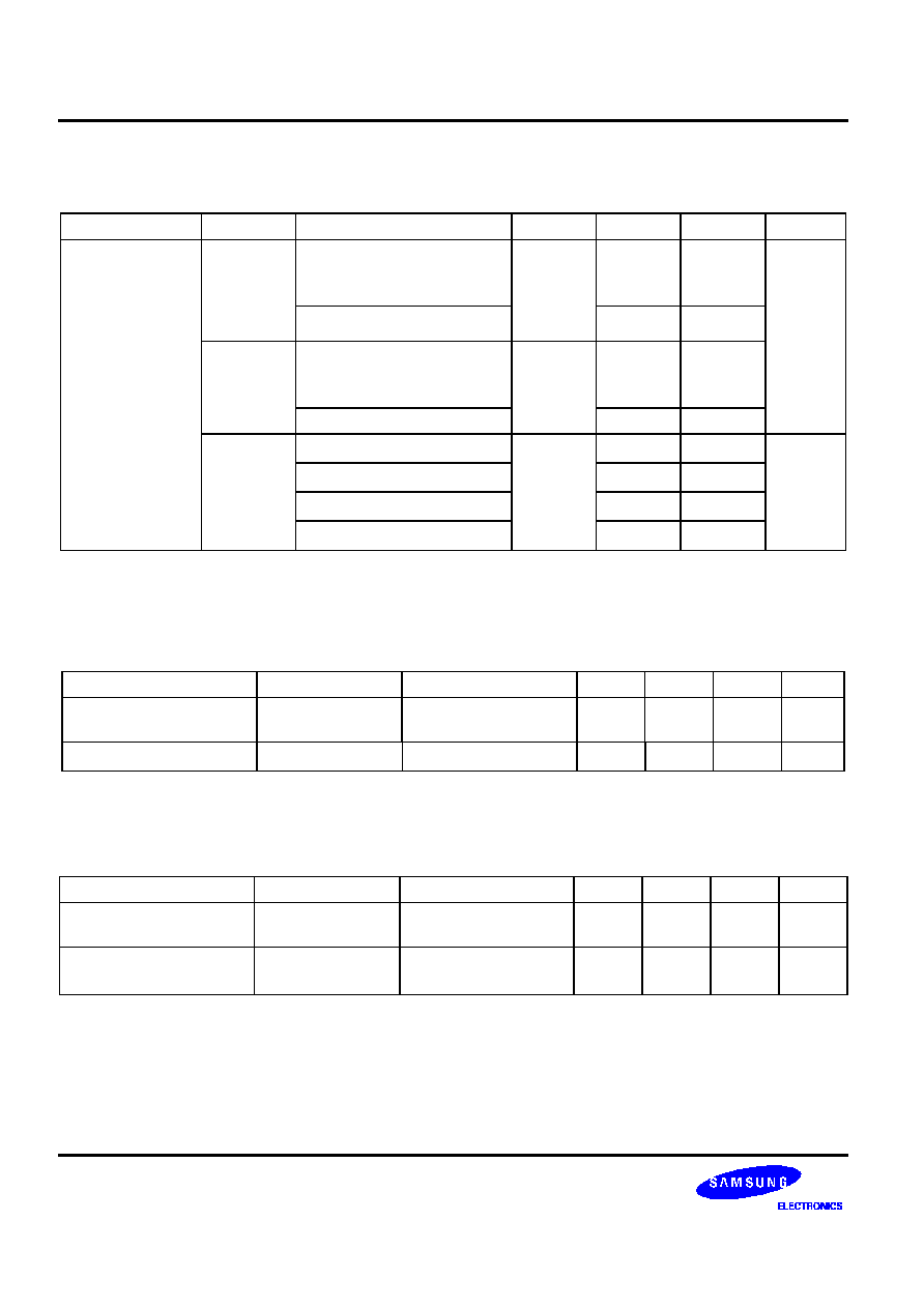
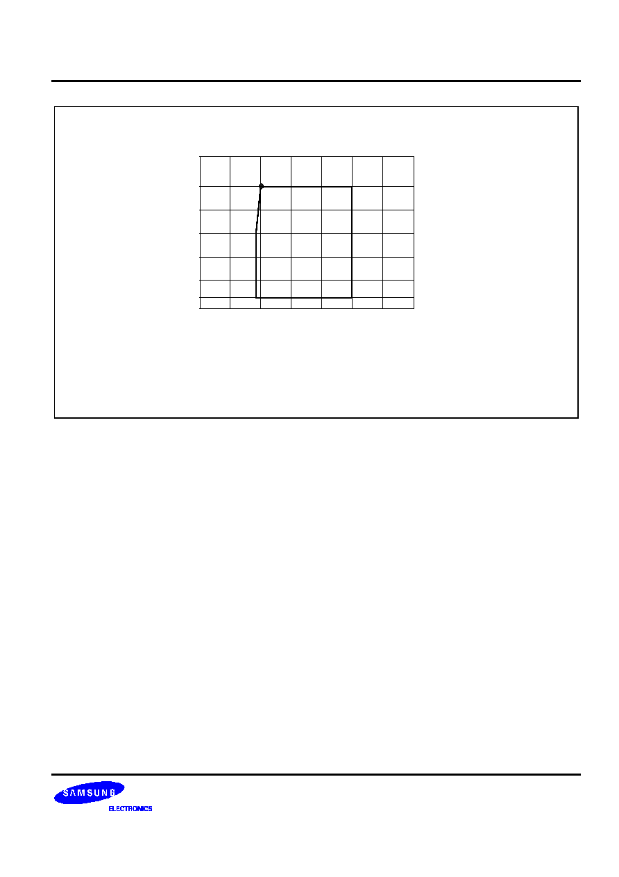
Execution of
STOP Instrction
~ ~
V
DDDR
~ ~
Stop Mode
Idle Mode
(Basic Timer Active)
Data Retention Mode
t
WAIT
EXT INT
V
DD
Normal
Operating
Mode
0.2V
DD
0.8V
DD
Figure 14-1. Stop Mode Release Timing When Initiated by an External Interrupt
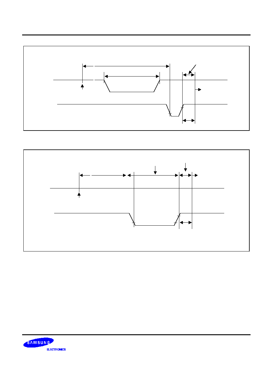
V
DD
~ ~
Normal
Operating
Mode
~ ~
Stop Mode
Oscillation Stabilization Time
t
WAIT
Reset
Occur
Execution of
STOP Instrction
RESET
NOTE
:
t
WAIT
is the same as 4096 x 16 x 1/f
OSC
.
Figure 14-2. Stop Mode Release Timing When Initiated by a
RESET
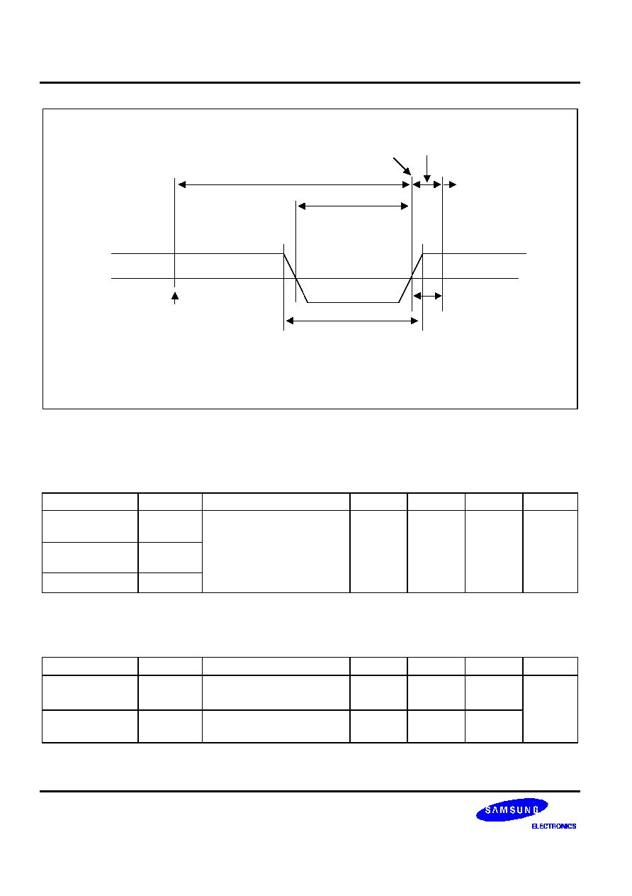
ELECTRICAL DATA
S3C80F7/C80F9/C80G7/C80G9 (KS88C01524/C01532/C01624/C01632)
14-6
Normal
Operating
Mode
~ ~
Stop Mode
Oscillation Stabilization Time
Reset
Occur
Execution of
STOP Instrction
V
DD
NOTE
:
t
WAIT
is the same as 4096 x 16 x 1/f
OSC
.
V
LVD
~ ~
Data Retention Time
V
DDDR
Back-up Mode
t
WAIT
Figure 14-3. Stop Mode Release Timing When Initiated by a LVD
Table 14-5. Input/Output Capacitance
(T
A
= ≠ 40
∞
C to + 85
∞
C , V
DD
=
0 V)
Parameter
Symbol
Conditions
Min
Typ
Max
Unit
Input
capacitance
C
IN
f = 1 MHz; unmeasured pins
are connected to V
SS
≠
≠
10
pF
Output
capacitance
C
OUT
I/O capacitance
C
IO
Table 14-6. A.C. Electrical Characteristics
(T
A
= ≠ 40
∞
C to + 85
∞
C)
Parameter
Symbol
Conditions
Min
Typ
Max
Unit
Interrupt input,
High, Low width
t
INTH
,
t
INTL
P0.0≠P0.7, P2.3≠P2.0
V
DD
= 5.0 V
200
300
≠
ns
RESET
input Low
width
t
RSL
Input
V
DD
= 5.0 V
1000
≠
≠
S3C80F7/C80F9/C80G7/C80G9 (KS88C01524/C01532/C01624/C01632)
ELECTRICAL DATA
14-7
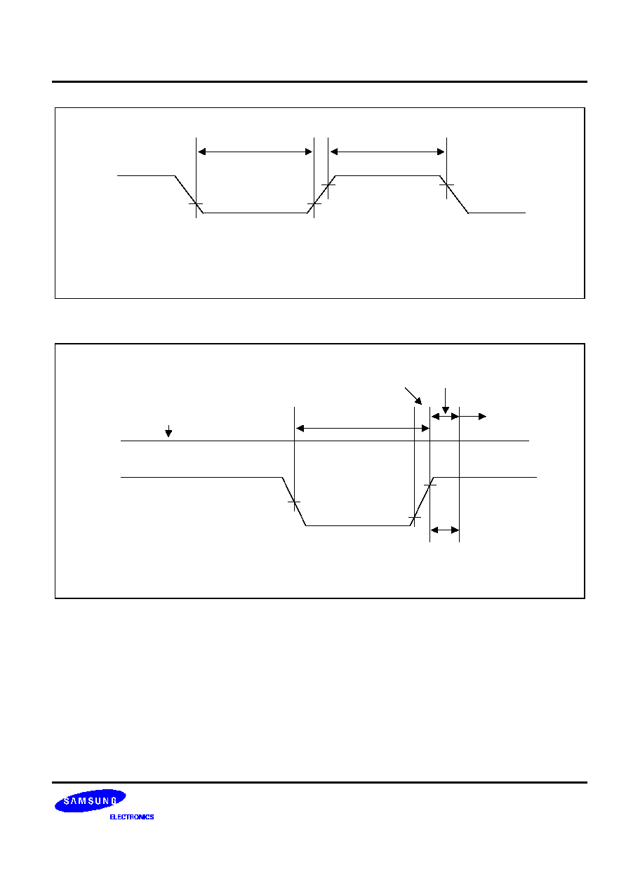
t
INTH
t
INTL
0.8 V
DD
0.2 V
DD
NOTE
:
The unit t
CPU
means one CPU clock period.
Figure 14-4. Input Timing for External Interrupts (Port 0, P2.3≠P2.0)
Normal
Operating
Mode
Oscillation Stabilization Time
Reset
Occur
V
DD
NOTE
:
t
WAIT
is the same as 4096 x 16 x 1/f
OSC
.
RESET
t
WAIT
Normal Operating Mode
Back-up Mode
(Stop Mode)
Figure 14-5. Input Timing for
RESET
ELECTRICAL DATA
S3C80F7/C80F9/C80G7/C80G9 (KS88C01524/C01532/C01624/C01632)
14-8
Table 14-7. Oscillation Characteristics
(T
A
= ≠ 40
∞
C + 85
∞
C)
Oscillator
Clock Circuit
Conditions
Min
Typ
Max
Unit
Crystal
X
IN
C1
C2
X
OUT
CPU clock oscillation
frequency
1
≠
8
MHz
Ceramic
X
IN
C1
C2
X
OUT
CPU clock oscillation
frequency
1
≠
8
MHz
External clock
X
IN
X
OUT
S3C80F9
External
Clock
Open Pin
X
IN
input frequency
1
≠
8
MHz
Table 14-8. Oscillation Stabilization Time
(T
A
= ≠ 40
∞
C + 85
∞
C, V
DD
= 4.5 V to 5.0 V)
Oscillator
Test Condition
Min
Typ
Max
Unit
Main crystal
f
OSC
> 400 kHz
≠
≠
20
ms
Main ceramic
Oscillation stabilization occurs when V
DD
is
equal to the minimum oscillator voltage range.
≠
≠
10
ms
External clock
(main system)
X
IN
input High and Low width (t
XH
, t
XL
)
25
≠
500
ns
Oscillator
stabilization
wait time
t
WAIT
when released by a reset
(1)
≠
2
16
/f
OSC
≠
ms
t
WAIT
when released by an interrupt
(2)
≠
≠
≠
ms
NOTES:
1.
f
OSC
is the oscillator frequency.
2.
The duration of the oscillation stabilization time (t
WAIT
) when it is released by an interrupt is determined by the setting
in the basic timer control register, BTCON.
S3C80F7/C80F9/C80G7/C80G9 (KS88C01524/C01532/C01624/C01632)
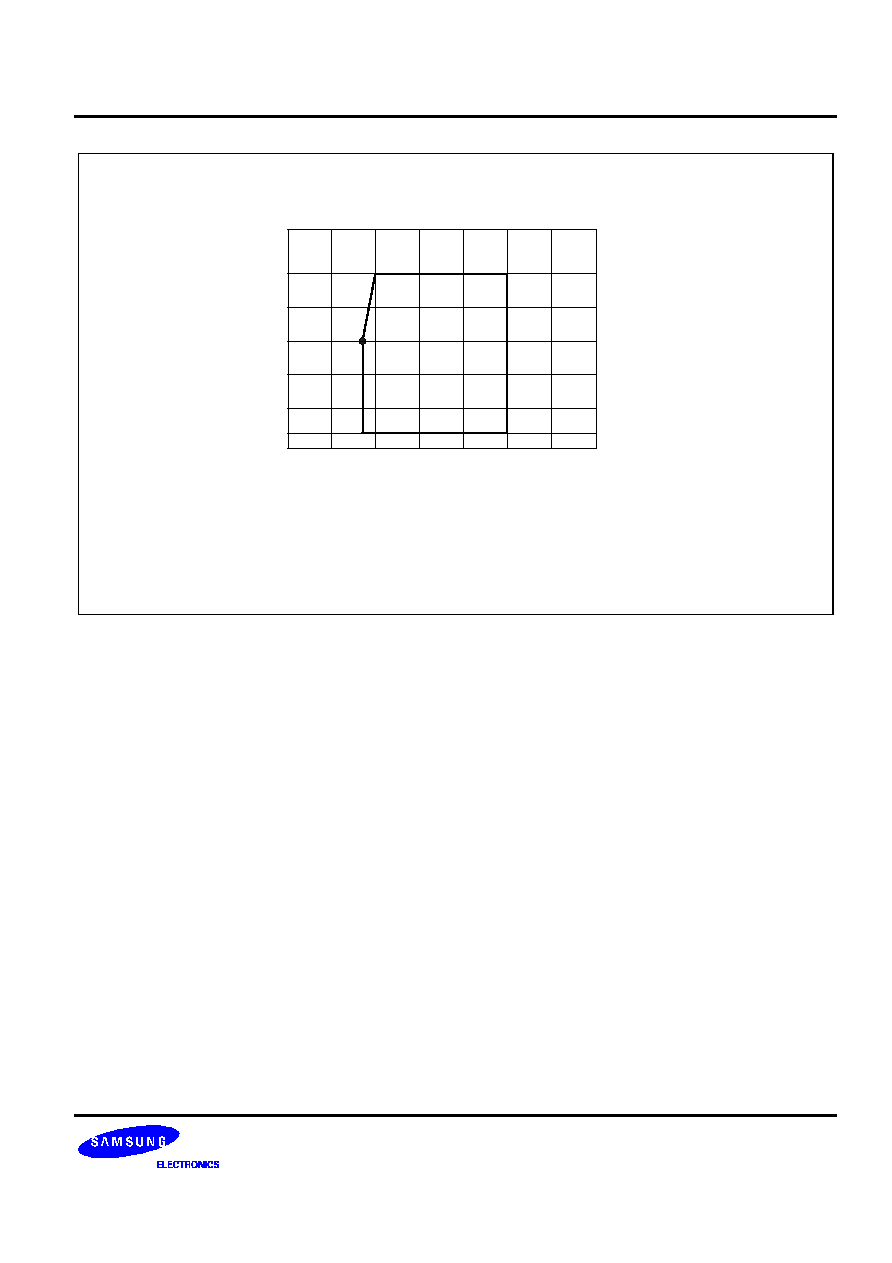
ELECTRICAL DATA
14-9
Instruction
Clock
100 kHz
fOSC
(Main Oscillator
Frequency)
1
2
3
4
5
Supply Voltage (V)
Instruction Clock = 1/6n x oscillator frequency (n = 1, 2, 8, or 16)
A: 2.0 V, 8 MHz
250 kHz
500 kHz
1.0 MHz
1.25 MHz
2 MHz
A
8 MHz
6 MHz
4 MHz
400 kHz
6
7
Figure 14-6. Operating Voltage Range of S3C80F9
S3C80F7/C80F9/C80G7/C80G9 (KS88C01524/C01532/C01624/C01632)
ELECTRICAL DATA
15-1
15
ELECTRICAL DATA 2 (S3C80G7/C80G9)
OVERVIEW
In this section, S3C80G7/C80G9 electrical characteristics are presented in tables and graphs. The information is
arranged in the following order:
-- Absolute maximum ratings
-- D.C. electrical characteristics
-- Data retention supply voltage in Stop mode
-- Stop mode release timing when initiated by an external interrupt
-- Stop mode release timing when initiated by a Reset
-- I/O capacitance
-- A.C. electrical characteristics
-- Input timing for external interrupts
-- Input timing for
RESET
-- Oscillation characteristics
-- Oscillation stabilization time
ELECTRICAL DATA
S3C80F7/C80F9/C80G7/C80G9 (KS88C01524/C01532/C01624/C01632)
15-2
Table 15-1. Absolute Maximum Ratings
(T
A
= 25
∞
C)
Parameter
Symbol
Conditions
Rating
Unit
Supply voltage
V
DD
≠
≠ 0.3 to + 6.5
V
Input voltage
V
IN
≠
≠ 0.3 to
V
DD
+ 0.3
V
Output voltage
V
O
All output pins
≠ 0.3 to V
DD
+ 0.3
V
Output current High
I
OH
One I/O pin active
≠ 18
mA
All I/O pins active
≠ 60
Output current Low
I
OL
One I/O pin active
+ 30
mA
Total pin current for ports 0, 1, and 2
+ 100
Total pin current for port 3
+ 40
Operating
temperature
T
A
≠
≠ 40 to + 85
∞
C
Storage temperature
T
STG
≠
≠ 65 to + 150
∞
C
Table 15-2. D.C. Electrical Characteristics
(T
A
= ≠ 40
∞
C to + 85
∞
C, V
DD
= 2.0 V to 5.0 V)
Parameter
Symbol
Conditions
Min
Typ
Max
Unit
Operating Voltage
V
DD
F
OSC
= 4 MHz
(Instruction clock = 1 MHz)
1.7
≠
5.0
V
Input High
voltage
V
IH1
All input pins except V
IH2
and V
IH3
0.8 V
DD
≠
V
DD
V
V
IH2
RESET
0.85 V
DD
V
DD
V
IH3
XIN
V
DD
≠ 0.3
V
DD
Input Low voltage
V
IL1
All input pins except V
IL2
and V
IL3
0
≠
0.2 V
DD
V
V
IL2
RESET
0.2 V
DD
V
IL3
XIN
0.3
Output High
voltage
V
OH1
V
DD
= 2.4 V I
OH
= ≠ 6 mA
Port 3.1 only, TA = 25
∞
C
V
DD
≠ 0.7
V
V
OH2
V
DD
= 2.4 V, I
OH
= ≠ 2.2mA
P3.0, P2.0≠2.3
T
A
= 25
∞
C
V
DD
≠ 0.7
S3C80F7/C80F9/C80G7/C80G9 (KS88C01524/C01532/C01624/C01632)
ELECTRICAL DATA
15-3
Table 15-2. D.C. Electrical Characteristics (Continued)
(T
A
= ≠ 40
∞
C to + 85
∞
C, V
DD
= 2.0 V to 5.0 V)
Parameter
Symbol
Conditions
Min
Typ
Max
Unit
Output High
voltage
V
OH3
V
DD
= 2.4 V,I
OH
= ≠ 1 mA
Port0, Port1, P2.4≠2.7 and Port4
T
A
= 25
∞
C
V
DD
≠
1.0
≠
≠
V
Output Low
voltage
V
OL1
V
DD
= 2.4 V, I
OL
= 12 mA, port
3.1 only, T
A
= 25
∞
C
≠
0.4
0.5
V
V
OL2
V
DD
= 2.4 V, I
OL
= 5 mA
P3.0, P3.4≠3.5, P2.0≠2.3
T
A
= 25
∞
C
0.4
0.5
V
OL3
I
OL
= 2mA
Port 0, Port1, P2.4≠2.7 and Port4
T
A
= 25
∞
C
0.4
1
Input High
leakage current
I
LIH1
V
IN
= V
DD
All input pins except X
IN
and
X
OUT
≠
≠
1
µA
I
LIH2
V
IN
= V
DD
, X
IN
and X
OUT
20
Input Low
leakage current
I
LIL1
V
IN
= 0 V
All input pins except X
IN
, X
OUT
,
and
RESET
≠
≠
≠ 1
µA
I
LIL2
V
IN
= 0 V
X
IN
and X
OUT
≠ 20
Output High
leakage current
I
LOH
V
OUT
= V
DD
All output pins
≠
≠
1
µA
Output Low
leakage current
I
LOL
V
OUT
= 0 V
All output pins
≠
≠
≠ 1
µA
Pull-up resistors
R
L1
V
IN
= 0 V, V
DD
= 2.4 V
T
A
= 25
∞
C, Ports 0≠2, P3.2≠3.3
44
55
95
k
ELECTRICAL DATA
S3C80F7/C80F9/C80G7/C80G9 (KS88C01524/C01532/C01624/C01632)
15-4
Table 15-2. D.C. Electrical Characteristics (Continued)
(T
A
= ≠ 40
∞
C to + 85
∞
C, V
DD
= 2.0 V to 5.0 V)
Parameter
Symbol
Conditions
Min
Typ
Max
Unit
Supply current
(note)
I
DD1
Operating mode
V
DD
= 5.0 V
4 MHz crystal
≠
4.5
9
mA
I
DD2
Idle mode
V
DD
= 5.0 V
4 MHz crystal
1.6
3.0
I
DD3
Stop mode;
V
DD
= 5.0 V
≠
1
6
uA
NOTE: Supply current does not include current drawn through internal pull-up resistors or external output current loads.
Table 15-3. Characteristics of Low Voltage Detect circuit
(T
A
= ≠ 40
∞
C to + 85
∞
C)
Parameter
Symbol
Conditions
Min
Typ
Max
Unit
Hysteresys Voltage of
LVD (Slew Rate of LVD)
V
≠
≠
100
300
mV
Low level detect voltage
V
LVD
≠
1.70
1.90
2.10
V
Table 15-4. Data Retention Supply Voltage in Stop Mode
(T
A
= ≠ 40
∞
C to + 85
∞
C)
Parameter
Symbol
Conditions
Min
Typ
Max
Unit
Data retention supply
voltage
V
DDDR
≠
1.0
≠
5.0
V
Data retention supply
current
I
DDDR
V
DDDR
= 1.0 V
Stop mode
≠
≠
1
µA

S3C80F7/C80F9/C80G7/C80G9 (KS88C01524/C01532/C01624/C01632)
ELECTRICAL DATA
15-5
Execution of
STOP Instrction
~ ~
V
DDDR
~ ~
Stop Mode
Idle Mode
(Basic Timer Active)
Data Retention Mode
t
WAIT
EXT INT
V
DD
Normal
Operating
Mode
0.2V
DD
0.8V
DD
Figure 15-1. Stop Mode Release Timing When Initiated by an External Interrupt
V
DD
~ ~
Normal
Operating
Mode
~ ~
Stop Mode
Oscillation Stabilization Time
t
WAIT
Reset
Occur
Execution of
STOP Instrction
RESET
NOTE
:
t
WAIT
is the same as 4096 x 16 x 1/f
OSC
.
Figure 15-2. Stop Mode Release Timing When Initiated by a
RESET
ELECTRICAL DATA
S3C80F7/C80F9/C80G7/C80G9 (KS88C01524/C01532/C01624/C01632)
15-6
Table 15-5. Input/Output Capacitance
(T
A
= ≠ 40
∞
C to + 85
∞
C , V
DD
=
0 V)
Parameter
Symbol
Conditions
Min
Typ
Max
Unit
Input
capacitance
C
IN
f = 1 MHz; unmeasured pins
are connected to V
SS
≠
≠
10
pF
Output
capacitance
C
OUT
I/O capacitance
C
IO
Table 15-6. A.C. Electrical Characteristics
(T
A
= ≠ 40
∞
C to + 85
∞
C)
Parameter
Symbol
Conditions
Min
Typ
Max
Unit
Interrupt input,
High, Low width
t
INTH
,
t
INTL
P0.0≠P0.7, P2.3≠P2.0
V
DD
= 5.0 V
200
300
≠
ns
RESET
input Low
width
t
RSL
Input
V
DD
= 5.0 V
1000
≠
≠

S3C80F7/C80F9/C80G7/C80G9 (KS88C01524/C01532/C01624/C01632)
ELECTRICAL DATA
15-7
t
INTH
t
INTL
0.8 V
DD
0.2 V
DD
NOTE
:
The unit t
CPU
means one CPU clock period.
Figure 15-3. Input Timing for External Interrupts (Port 0, P2.3≠P2.0)
Normal
Operating
Mode
Oscillation Stabilization Time
Reset
Occur
V
DD
NOTE
:
t
WAIT
is the same as 4096 x 16 x 1/f
OSC
.
RESET
t
WAIT
Normal Operating Mode
Back-up Mode
(Stop Mode)
Figure 15-4. Input Timing for
RESET
ELECTRICAL DATA
S3C80F7/C80F9/C80G7/C80G9 (KS88C01524/C01532/C01624/C01632)
15-8
Table 15-7. Oscillation Characteristics
(T
A
= ≠ 40
∞
C + 85
∞
C)
Oscillator
Clock Circuit
Conditions
Min
Typ
Max
Unit
Crystal
X
IN
C1
C2
X
OUT
CPU clock oscillation
frequency
1
≠
4
MHz
Ceramic
X
IN
C1
C2
X
OUT
CPU clock oscillation
frequency
1
≠
4
MHz
External clock
X
IN
X
OUT
S3C80G9
External
Clock
Open Pin
X
IN
input frequency
1
≠
4
MHz
Table 15-8. Oscillation Stabilization Time
(T
A
= ≠ 40
∞
C + 85
∞
C, V
DD
= 4.5 V to 5.0 V)
Oscillator
Test Condition
Min
Typ
Max
Unit
Main crystal
f
OSC
> 400 kHz
≠
≠
20
ms
Main ceramic
Oscillation stabilization occurs when V
DD
is
equal to the minimum oscillator voltage range.
≠
≠
10
ms
External clock
(main system)
X
IN
input High and Low width (t
XH
, t
XL
)
25
≠
500
ns
Oscillator
stabilization
wait time
t
WAIT
when released by a reset
(1)
≠
2
16
/f
OSC
≠
ms
t
WAIT
when released by an interrupt
(2)
≠
≠
≠
ms
NOTES:
1.
f
OSC
is the oscillator frequency.
2.
The duration of the oscillation stabilization time (t
WAIT
) when it is released by an interrupt is determined by the setting
in the basic timer control register, BTCON.
S3C80F7/C80F9/C80G7/C80G9 (KS88C01524/C01532/C01624/C01632)
ELECTRICAL DATA
15-9
Instruction
Clock
100 kHz
fOSC
(Main Oscillator
Frequency)
1
2
3
4
5
Supply Voltage (V)
Instruction Clock = 1/6n x oscillator frequency (n = 1, 2, 8, or 16)
A: 1.7 V, 4 MHz
250 kHz
500 kHz
1.0 MHz
1.25 MHz
2 MHz
A
8 MHz
6 MHz
4 MHz
400 kHz
6
7
Figure 15-6. Operating Voltage Range of S3C80G9
S3C80F7/C80F9/C80G7/C80G9 (KS88C01524/C01532/C01624/C01632)
MECHANICAL DATA
16-1
16
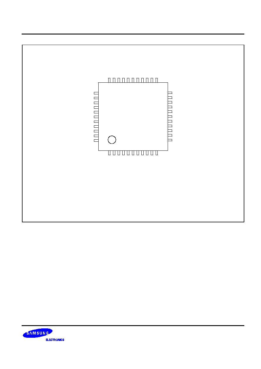
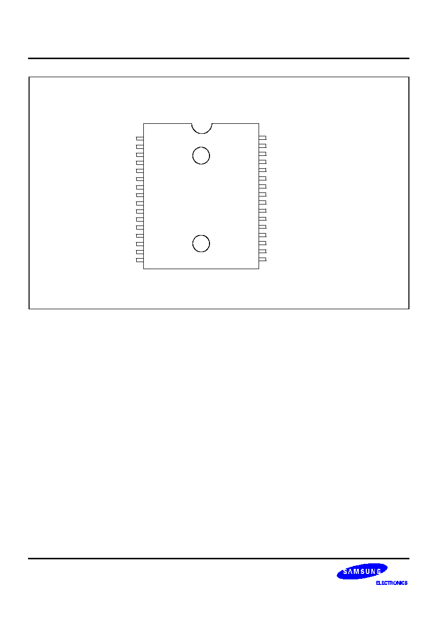
MECHANICAL DATA
OVERVIEW
The S3C80F7/C80F9/C80G7/C80G9 microcontroller is currently available in a 32-pin SOP, 42-pin SDIP and 44-
pin QFP package.
32-SOP-450A
20.30 MAX
19.90
± 0.20
#17
#16
0-8
0.25
+ 0.10
- 0.05
11.43
8.34
±
0.20
0.90
±
0.20
0.05 MIN
2.00
±
0.10
2.20 MAX
0.10 MAX
1.27
NOTE: Dimensions are in millimeters.
12.00
±
0
.30
#32
#1
(0.43)
0.40
± 0.10
Figure 16-1. 32-Pin SOP Package Dimension
MECHANICAL DATA
S3C80F7/C80F9/C80G7/C80G9 (KS88C01524/C01532/C01624/C01632)
16-2
NOTE: Dimensions are in millimeters.
39.50 MAX
39.10
± 0.20
0.50
±
0.10
1.78
(1.77)
0.51 MIN
3.30
± 0.30
3.50
±
0.20
5.08 MAX
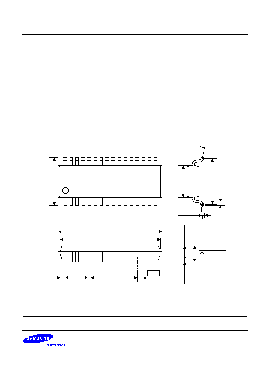
42-SDIP-600
0-15
1.00
±
0.10
0.25
+ 0.10- 0.05
15.24
14.00
±
0
.20
#42
#22
#21
#1
Figure 16-2. 42-Pin SDIP Package Dimension
S3C80F7/C80F9/C80G7/C80G9 (KS88C01524/C01532/C01624/C01632)
MECHANICAL DATA
16-3
44-QFP-1010B
#44
NOTE: Dimensions are in millimeters.
10.00
± 0.20
13.20
± 0.30
10.00
± 0.20
13.20
± 0.30
#1
0.35
+ 0.10
- 0.05
0.80
0.10 MAX
0.80 ± 0.20
0.05 MIN
2.05
± 0.10
2.30 MAX
0.15
+ 0.10
- 0.05
0-8
0.15 MAX
(1.00)
Figure 16-3. 44-Pin SQFP Package Dimension