KS88C6216/C6224/C6232/P6232
PRODUCT OVERVIEW
1-1
1
PRODUCT OVERVIEW
SAM8 PRODUCT FAMILY
Samsung's SAM8 family of 8-bit single-chip CMOS microcontrollers offers a fast and efficient CPU with a wide
range of integrated peripherals, in various mask-programmable ROM sizes. Analog its major CPU features are:
-- Efficient register-oriented architecture
-- Selectable CPU clock sources
-- Idle and Stop power-down mode release by interrupt
-- Built-in basic timer with watchdog function
The sophisticated interrupt structure recognizes up to eight interrupt levels. Each level can have one or more
interrupt sources and vectors. Fast interrupt processing (within a minimum of six CPU clocks) can be assigned to
specific interrupt levels.
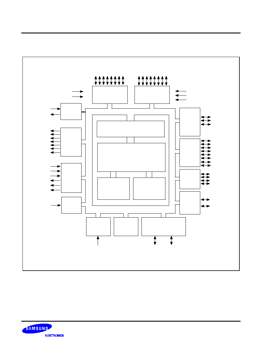
KS88C6216/C6224/C6232/P6232 MICROCONTROLLERS
KS88C6216/C6224/C6232/P6232 single-chip 8-bit
microcontrollers are based on the powerful SAM8
CPU architecture. The internal register file is logically
expanded to increase the on-chip register space.
KS88C6216/C6224/C6232/P6232 contain 16/32 K
bytes of on-chip program ROM.
In line with Samsung's modular design approach, the
following peripherals are integrated with the SAM8
core:
-- Four programmable I/O ports (total 27 pins)
-- One 8-bit basic timer for oscillation stabilization
and watchdog functions
-- One 8-bit general-purpose timer/counter with
selectable clock sources
-- One 12-bit counter with selectable clock sources,
including Hsync or Csync input
-- One interval timer
-- PWM block with seven 8-bit PWM circuits
-- Sync processor block (for Vsync and Hsync I/O,
Csync input, and Clamp signal output)
-- DDC and normal Multi-master IIC-bus
-- 4-channel A/D converter (8-bit resolution)
KS88C6216/C6224/C6232/P6232 are a versatile
microcontrollers which are ideal for use in multi-sync
monitors or in general-purpose applications that
require sophisticated timer/counter, PWM, sync
signal processing, A/D converter, and multi-master
IIC-bus support with DDC. They are available in a 42-
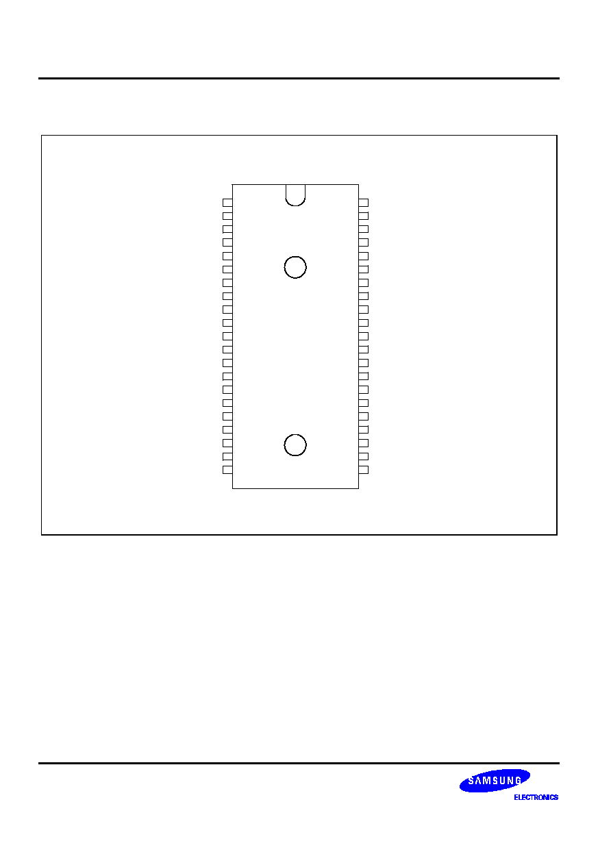
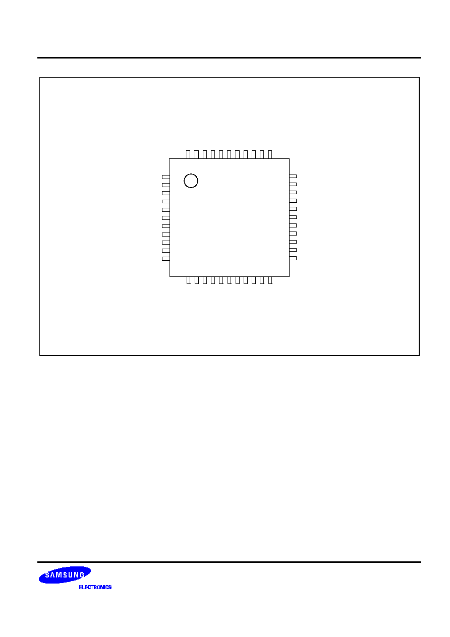
pin SDIP or a 44-pin QFP package.
OTP
KS88C6216/C6224/C6232 microcontrollers are also available in OTP (One Time Programmable) version named,
KS88P6232. KS88P6232 microcontroller has an on-chip 32-Kbyte one-time-programmable EPROM instead of
masked ROM. KS88P6232 is comparable to KS88C6216/C6224/C6232, both in function and pin configuration
except its ROM size.

PRODUCT OVERVIEW
KS88C6216/C6224/C6232/P6232
1-2
FEATURES
CPU
�
SAM8 CPU core
Memory
�
16/24/32-Kbyte internal program memory (ROM)
�
464-byte general-purpose register area
Instruction Set
�
78 instructions
�
IDLE and STOP instructions added for
power-down modes
Instruction Execution Time
�
Minimum 500 ns (with 12 MHz CPU clock)
Interrupts
�
Ten interrupt sources
�
Ten interrupt vectors
�
Seven interrupt level
�
Fast interrupt feature
General I/O
�
Four I/O Ports (total 27pins)
8-Bit Basic Timer
�
Programmable timer for oscillation stabilization
interval control or watchdog timer function
�
Three selective internal clock frequencies
Timer/Counters
�
One 8-bit Timer/Counter with several clock
sources (Capture mode)
�
One 12-bit Counter with H-sync and several clock
sources
�
One Interval Timer
Pulse Width Modulator (PWM)
�
8-bit PWM: 7-CH
Sync-Processor Block
�
Vsync-I, Hsync-I, Csync-I input and Vsync-O,
Hsync-O, Clamp-O output pins
�
Pseudo sync signal output
�
Auto SOG detection
�
Auto Hsync polarity detection
DDC Multi-Master IIC-Bus 1-Ch
�
Serial Peripheral Interface
�
Support for Display Data Channel
(DDC1/DDC2B/DDC2Bi/DDC2B+)
Normal Multi-Master IIC-Bus 1-Ch
�
Serial Peripheral Interface
A/D Converter
�
4-channel; 8-bit resolution
Oscillator Frequency
�
8 MHz to 12 MHz crystal operation
�
Internal Max. 12 MHz CPU clock
Operating Temperature Range
�
� 40
�
C to + 85
�
C
Operating Voltage Range
�
4.0 V to 5.5 V
Package Types
�
42-pin SDIP, 44-pin QFP