
184pin Unbuffered DDR SDRAM MODULE
M368L3313BT1
Rev. 0.9 June. 2001
128MB DDR SDRAM MODULE
Unbuffered 184pin DIMM
(32Mx64(16Mx64*2 bank) based on 16Mx8 DDR SDRAM)
64-bit Non-ECC/Parity
Revision 0.9
June. 2001
184pin Unbuffered DDR SDRAM MODULE
M368L3313BT1
Rev. 0.9 June. 2001
Revision History
Revision 0 (Aug 1998)
1. First release for internal usage
Revision 0.1 (May. 1999)
1. Changed die revision from B-die to C-die
2. Changed DC/AC characteristics item from old version.
Revision 0.2 (Aug. 1999)
1. Changed die revision from C-die to B-die
2. Modified binning policy
From To
-Z (133Mhz) -Z (133Mhz/266Mbps@CL=2)
-8 (125Mhz) -Y (133Mhz/266Mbps@CL=2.5)
-0 (100Mhz) -0 (100Mhz/200Mbps@CL=2)
3.Modified the following AC spec values
*1
: Changed description method for the same functionality. This means no difference from the previous version.
4.Changed the following AC parameter symbol From tDQCK To tAC
Output data access time from CK/CK
Revision 0.3 (Sept. 1999)
1. Changed the odering information.
1-1. Exclude KM mark.
From To
KMM368... M368.....
1-2. PCB Revison
From To
- Blank: 1st generation - 0: 1st gernation
- A : 2nd generation - 1: 2nd generation
- B : 2nd generation - 2: 3nd generation
Example:KMM368L3313BT M368L3313BT0
1-3. Modified binning policy
From To
- 0 (100Mhz/200Mbps@CL=2) - A0 (100Mhz/200Mbps@CL=2)
- Z (133Mhz/266Mbps@CL=2) - A2 (133Mhz/266Mbps@CL=2)
- Y (133Mhz/266Mbps@CL=2.5) - B0 (133Mhz/266Mbps@CL=2.5)
From.
To.
-Z
-0
-Z
-Y
-0
tAC
+/- 0.75ns
+/- 1ns
+/- 0.75ns
+/- 0.75ns
+/- 0.8ns
tDQSCK
+/- 0.75ns
+/- 1ns
+/- 0.75ns
+/- 0.75ns
+/- 0.8ns
tDQSQ
+/- 0.5ns
+/- 0.75ns
+/- 0.5ns
+/- 0.5ns
+/- 0.6ns
tDS/tDH
0.5 ns
0.75 ns
0.5 ns
0.5 ns
0.6 ns
tCDLR
*1
2.5tCK-tDQSS
2.5tCK-tDQSS
1tCK
1tCK
1tCK
tPRE
*1
1tCK +/- 0.75ns
1tCK +/- 1ns
0.9/1.1 tCK
0.9/1.1 tCK
0.9/1.1 tCK
tRPST
*1
tCK/2 +/- 0.75ns
tCK/2 +/- 1ns
0.4/0.6 tCK
0.4/0.6 tCK
0.4/0.6 tCK
tHZQ
*1
tCK/2 +/- 0.75ns
tCK/2 +/- 1ns
+/- 0.75ns
+/- 0.75ns
+/-0.8ns

184pin Unbuffered DDR SDRAM MODULE
M368L3313BT1
Rev. 0.9 June. 2001
Revision 0.4 (December. 1999)
1. Changed from 3.3V to 2.5V in VDDSPD power.
Revision 0.5 (April. 2000)
< Page 3 >
1. Changed from 1450mil to 1250mil in PCB height.
2. Changed pin 90 from WP to NC in pin configuration table.
3. Changed in pin configuration table as followings.
pin 16 : CK0 -> CK1
pin 17 : CK0 -> /CK1
pin 137 : CK1 -> CK0
pin 138 : CK1 -> /CK0
4. Removed WP in pin description.
< Page 4>
5. Changed Clock wiring as followings.
CK0 / CK0 6SDRAMs -> 4SDRAMs
CK1 / CK1 4SDRAMs -> 6SDRAMs
6. Changed bypassing to reflect common Vdd/Vddq plane.
7. Added A13, BA1.
8. Removed WP from serial PD.
< Page 5>
9.
Changed Power & DC operating condition.
< Page 6 >
10. Added Overshoot/Undershoot spec
. Vih(max) = 4.2V, the overshoot voltage duration is
3ns at VDD.
. Vil(min) =- 1.5V, the overshoot voltage duration is
3ns at VSS.
< Page 6,7 >
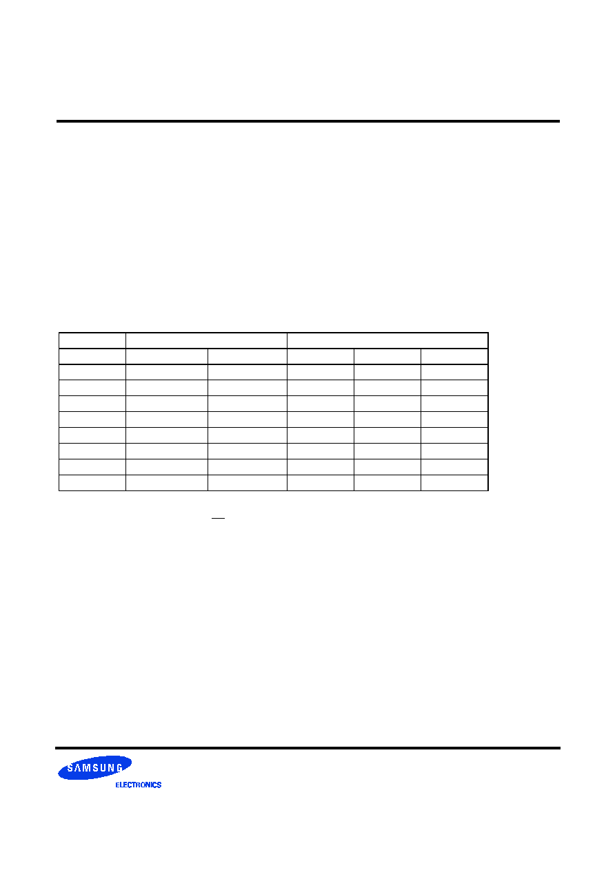
11. Changed AC operating conditions as follows.
Parameter
Symbol
From
To
Min
Max
Min
Max
I/O Reference voltage
V
REF
1.15
1.35
0.49*VDDQ
0.51*VDDQ
Input logic high voltage
V
IH
(DC)
V
REF
+0.18
V
DDQ
+0.3
V
REF
+0.15
V
DDQ
+0.3
Input logic low voltage
V
IL
(DC)
-0.3
V
REF
-0.18
-0.3
V
REF
-0.15
Input leakage current
I
I
-5
5
-2
2
Output High Current (V
OUT
= 1.95V)
I
OH
-15.2
-16.8
Output Low Current (V
OUT
= 0.35V)
I
OL
15.2
16.8
Parameter/Condition
Symbol
From
To
Min
Max
Min
Max
Input High (Logic 1) Voltage, DQ, DQS and DM signals VIH(AC)
VREF + 0.35
VREF + 0.31
Input Low (Logic 0) Voltage, DQ, DQS and DM signals. VIL(AC)
VREF - 0.35
VREF - 0.31
Input Differential Voltage, CK and CK inputs
VID(AC)
0.7
VDDQ+0.6
0.62
VDDQ+0.6

184pin Unbuffered DDR SDRAM MODULE
M368L3313BT1
Rev. 0.9 June. 2001
< Page 7 >
12. Changed Input/Output capacitance as follows.
< page 8, 9>
13. Changed AC parameters as follows.
14. Added AC parameters as follows
< Page 12>
15. Changed from 1450mil to 1250mil in Package dimension.
Revision 0.6 (June. 2000)
1. Changed PCB version from T0 to T1.
Parameter
Symbol
From
To
Min
Max
Min
Max
Input capacitance(A
0
~ A
11
, BA
0
~ BA
1
,RAS,CAS, WE )
C
IN1
-
90
65
81
Input capacitance(CKE
0,
CKE
1
)
C
IN2
-
62
42
50
Input capacitance(
CS
0
, CS
1
)
C
IN3
-
55
42
50
Input capacitance(
CLK
0
, CLK
1,
CLK
2
)
C
IN4
-
38
27
34
Data & DQS input/output capacitance(DQ
0
~DQ
63
)
C
OUT
-
16
10
13
Input capacitance(DM
0
~DM
8
)
C
IN5
-
16
10
13
Parameter
from
to
Comments
tDQSQ
+/- 0.5(PC266), +/- 0.6(PC200)
+0.5(PC266), +0.6(PC200)
tDV
+/- 0.35tCK
-
Removed
Parameter
Symbol
-A2(PC266@CL=2)
-B0(PC266@CL=2.5)
-A0(PC200@CL=2)
Min
Max
Min
Max
Min
Max
Output DQS valid window
tQH
tHPmin
-0.75ns
-
tHPmin
-0.75ns
-
tHPmin
-1.0ns
-
Clock half period
tHP
tCLmin
or
tCHmin
-
tCLmin
or
tCHmin
-
tCLmin
or
tCHmin
-
QFC setup to first DQS edge on reads
tQCS
0.9
1.1
0.9
1.1
0.9
1.1
QFC hold after last DQS edge on reads
tDQCH
0.4
0.6
0.4
0.6
0.4
0.6
Write command to QFC delay on write
tQCSW
4.0
4.0
4.0
Write burst end to QFC delay on write
tQCHW
1.25ns
0.5tCK
1.25ns
0.5tCK
1.25ns
0.5tCK
Write burst end to QFC delay on write
interrupted by Precharge
tQCHWI
1.25ns
1.5tCK
1.25ns
1.5tCK
1.25ns
1.5tCK

184pin Unbuffered DDR SDRAM MODULE
M368L3313BT1
Rev. 0.9 June. 2001
Revision 0.7 (October. 2000)
1.Added DC target spec values.
2.Deleted tDAL in AC parameter X.
Revision 0.8 (November. 2000)
1.Changed component placement on module PCB in package dimesions.
Revision 0.9 (June. 2001)
1. Changed module current speificaton
2. Changed typo size on module PCB in package dimesions. (from 2.6mm to 3mm).
3. Changed AC parameter table.