TV SOUND MPX FOR TWO CARRIER SYSTEM
S1A0688C01
1
INTRODUCTION
The S1A0688C01 is a monolithic integrated circuit designed for
demodulating two carrier TV-MPX broadcast.
FEATURES
∑
1st & 2nd Sound IF
∑
Double-PLL FM Detection
∑
AGC for CCA part
∑
Matrix for Multi-Sound Broadcasts
∑
Pilot Detector
∑
External Control Interface
∑
ID Indicators (Stereo, Bilingual)
∑
Available for Korea standard
∑
Non-clipping Output up to 400% modulation with AGC
∑
Available in DC control, Normal microcontroler control or IIC bus control systems
∑
ID output: Direct LED drive or IIC serial data output
∑
Non-adjust
ORDERING INFORMATION
Device
Package
Operating Temperature
S1A0688C01-A0B0
32
-
SDIP
-
400
-
10 to + 70
∞
C
32
-
SDIP
-
400
S1A0688C01
TV SOUND MPX FOR TWO CARRIER SYSTEM
2
BLOCK DIAGRAM
1
19
7
6
8
9
10
12
11
13
14
2
3
4
5
30
23
24
28
22
21
20
32
16
25
27
29
26
15
18
17
31
IF
IF
4.72MHz
1st PLL
4.5MHz
1st PLL
4.3MHz
VCO
A
A
30KHz
HPF
CCA
CCA
AGC
AMP
MATRIX
1/39
1/2
1/100
1/370
1/200
X20
100KHz
LPF
55.1KHz
SC BPF
AM DET
OFFSET CANCELLER
DN
CUT
COMP
MN
DET
DIGITAL FREQUENCY
DETECTOR
CONTROL TYPE
AUTO DETECT
U-COM INTERFACE
(DC/3-LINE U-COM/IIC-BUS)
ZAPPING
BLOCK
X3
276Hz
SC BPF
150Hz
SC BPF
390Hz
SC BPF
X8
VOLTAGE
REFERENCE
4.72MHz
2nd PLL
4.5MHz
2nd PLL
S1
S1
VCC
VDD
GND
VSS
CCA
PLL
TV SOUND MPX FOR TWO CARRIER SYSTEM
S1A0688C01
3
PIN CONFIGURATION
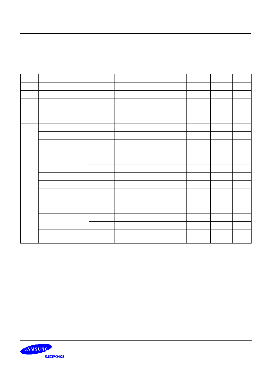
PIN DESCRIPTION
Pin No.
Description
Pin No.
Description
1
Analog GND
17
ID Filter Offset Canceling Cap.
2
SIF 2 Input
18
R Output
3
SIF 2 Bypass
19
Digital VSS
4
SIF 1 Bypass
20
Data Input / Output (SDA)
5
SIF 1 Input
21
Clock Input (SCL)
6
SIF 2 LPF Capacitor
22
Enable Input (EN)
7
SIF 1 LPF Capacitor
23
ID Indicator (Stereo)
8
SIF 1 Amplifier Capacitor
24
ID Indicator (Bilingual)
9
SIF 2 Amplifier Capacitor
25
Digital VDD
10
SIF 1 DET Output
26
AM DET Output
11
SIF 1 CCA Input
27
Frequency DET Input
12
SIF 2 DET Output
28
Slave Custom Code
13
SIF 2 CCA Input
29
External Clock In
14
AGC Detect Capacitor
30
Reference Clock Monitor
15
L output
31
Test Mode Switch
16
Analog VCC
32
Voltage Reference Capacitor
S1A0688C01
24
23
22
21
20
19
18
17
16
15
14
13
1
2
3
4
5
6
7
8
9
10
11
12
GND
26
25
28
27
30
29
32
31
IF2
BP2
BP1
IF1
LPC2
LPC1
AC1
AC2
S1O
S1I
S2O
AGC
S2I
LO
VCC
RC
TMS
RCM
ECI
SCC
FDI
ADO
VDD
BIB
STB
EN
SCL
VSS
SDA
RO
OFC
S1A0688C01
TV SOUND MPX FOR TWO CARRIER SYSTEM
4
ABSOLUTE MAXIMUM RATINGS
RECOMMENDED OPERATING CONDITIONS
Parameter
Symbol
Condition
Min.
Typ.
Max.
Unit
Maximum Supply voltage
VCC
max
Ta = 25
∞
C
V
I
= 0
-
-
6
V
Power Dissipation
P
D
-
-
1000
mW
Operating temperature
T
OPR
-
10
-
70
∞
C
Storage temperature
T
STG
-
40
-
125
∞
C
Parameter
Symbol
Condition
Min.
Typ.
Max.
Unit
Operating Voltage
V
OPR
-
4.7
5
5.5
V
TV SOUND MPX FOR TWO CARRIER SYSTEM
S1A0688C01
5
ELECTRICAL CHARACTERISTICS
DC Electrical Characteristics
(Ta = 25
∞
C, VCC = VDD = 5V, fm = 1kHz, V
I
= 80dB
µ
,
f =
±
25kHz, unless otherwise specified)
* : Pilot signal FM deviation is
±
2.5kHz after 50% AM modulation.
Parameter
Symbol
Condition
Min.
Typ.
Max.
Unit
ICC
Vi = 0
35
60
85
mA
IDD
Vi = 0
-
-
2.0
mA
SIF
Input Limiting Voltage
Vlim
-
-
-
50
dB
µ
AM Rejection Ratio
AMRR
AM 30% Mod
40
55
-
dB
Input Impedance
Zin
-
-
1
-
Kohm
PILOT
*
Pilot Input Sensitivity
Vps
-
-
-
50
dB
µ
ID ON time
Ton
MONO
ST, BI
-
1.0
1.5
SEC
ID OFF time
Toff
ST, BI
MONO
-
-
0.3
SEC
Output level
Vo
-
320
420
520
mVrms
Matrix
Matrix THD
THDm1
-
-
0.2
1.0
%
THDm2
f =
±
100kHz
-
0.5
5.0
%
Noise Output (RF off)
Voff
Carrier OFF
-
-
400
mVrms
Output Impedance
Zout
-
-
-
50
ohm
Separation Ratio
SEPtyp
non-adjust
25
-
-
dB
SEPadj
IIC Bus adjust
40
45
-
dB
Cross Talk
CT
f =
±
25kHz
50
55
-
dB
Matrix S/N Ratio
S/N
f =
±
25kHz
55
60
-
dB
S/N(st)
f =
±
25kHz (ST)
50
55
-
dB
MUTE Attenuation
Ratio
Amute
f =
±
25kHz
-
-
66
-
55
dB
S1A0688C01
TV SOUND MPX FOR TWO CARRIER SYSTEM
6
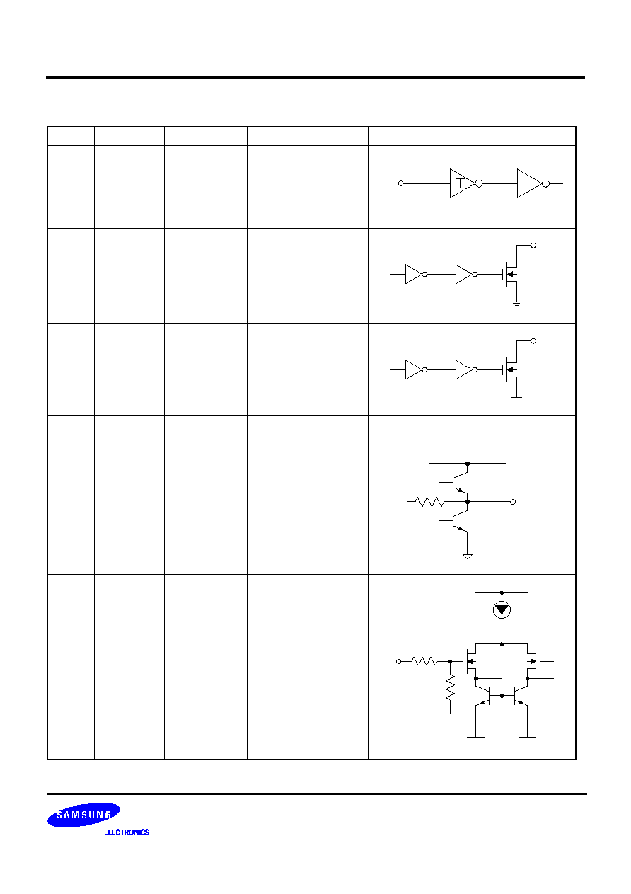
PIN DESCRIPTION
Pin No.
Symbol
Pin Name
Description
Internal Equivalence Circuit
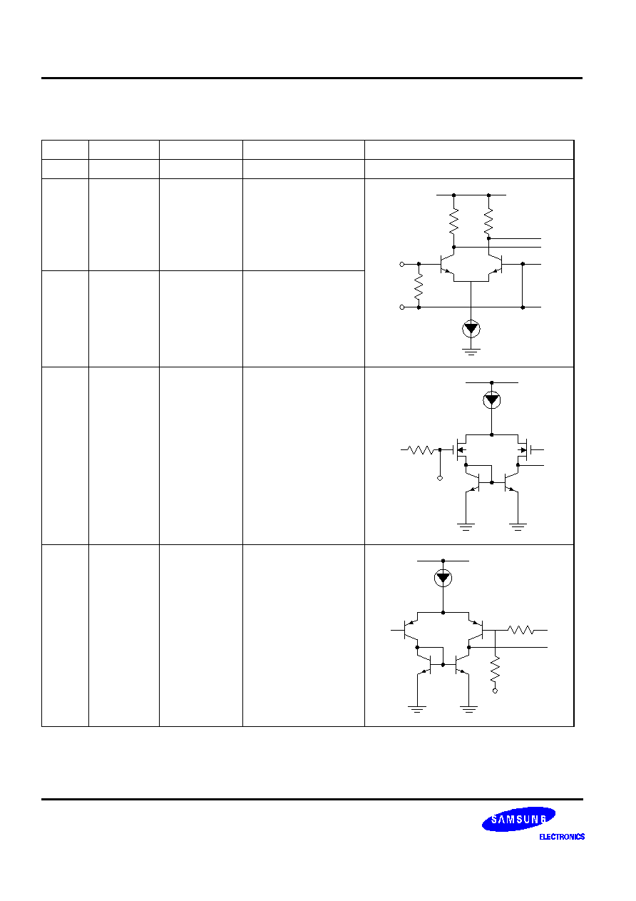
1
GND
Analog ground
-
-
2, 5
SIF2, SIF1
SIF input pin
SIF signal input through
a SIF filter
3, 4
BP2, BP1
IF bypass pin
IF Bypass pin is
grounded with a
capacitor
6, 7
LPC2, LPC1
PLL LPF pin
The external capacitor
extracts DC level from
the 1st PLL output of
FM DET.
8, 9
AC1, AC2
DET AMP NF
pin
Negative feedback pin
of FM DET amplifier
Grounded with a
capacitor
IF1
(IF2)
BP1
(BP2)
LPC1
(LPC2)
AC1
(AC2)
TV SOUND MPX FOR TWO CARRIER SYSTEM
S1A0688C01
7
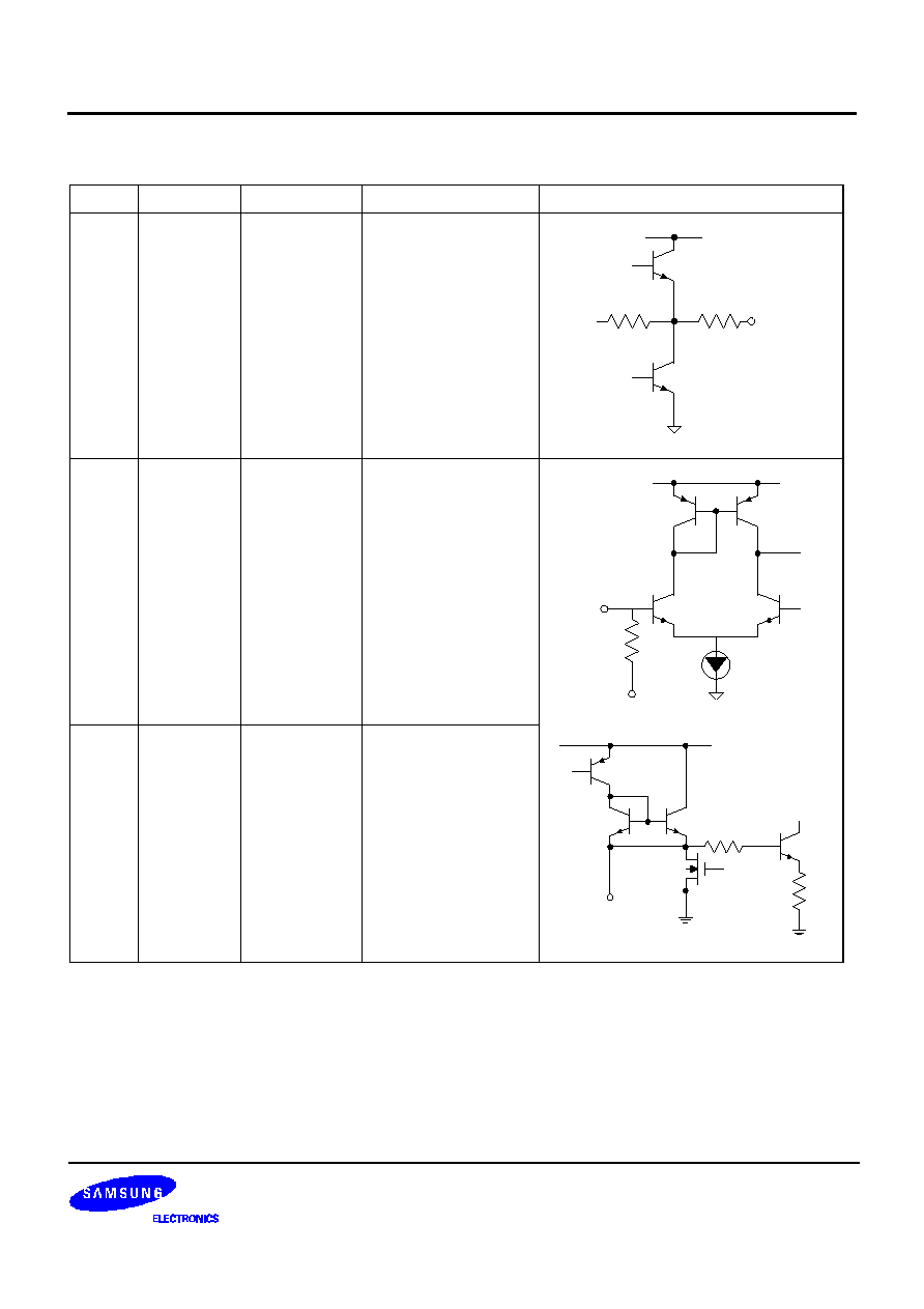
10, 12
S1O, S2O
FM DET output
FM DET output pin
connected with a de-
emphasis circuit
11, 13
S1I, S2I
FM detected
signal input pin
Input pin of current
control amplifier (CCA).
FM detected output
signal is added to this
pin.
14
AGC
AGC DET pin
AGC detect pin is
grounded through a
capacitor. If the signal
level is over the
predetermined value,
this terminal voltage will
be raised. AGC function
can be deactivated by
connect this terminal to
GND.
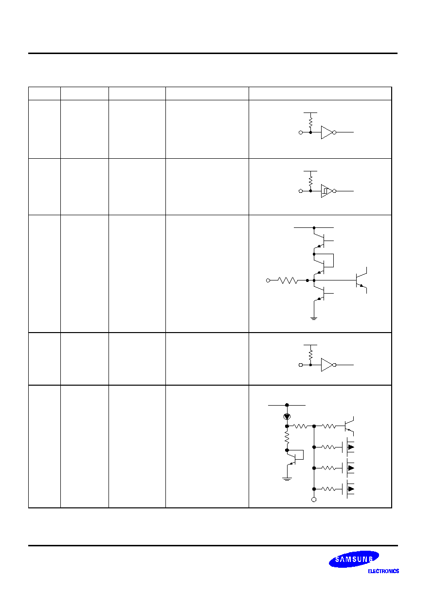
PIN DESCRIPTION
(Continued)
Pin No.
Symbol
Pin Name
Description
Internal Equivalence Circuit
S1O
(S2O)
S1I
(S2I)
BIAS
AGC
S1A0688C01
TV SOUND MPX FOR TWO CARRIER SYSTEM
8
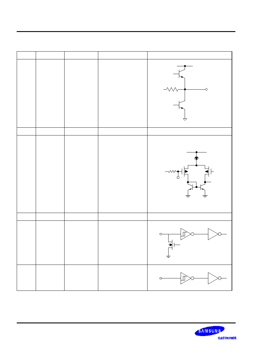
15, 18
LO, RO
Matrix output
pin
Audio output signal is
provided from this pin.
16
VCC
Analog power
-
-
17
OFC
ID BPF offset
cancel pin
The external capacitor
is used to eliminate
offset of ID filter
19
VSS
Digital ground
≠
≠
20
SDA
Serial data
input and
output
It is the data
communication line of
IIC bus used to
exchange the MICOM
data and IC internal
data.
21
SCL
Clock signal
CLOCK line of IIC bus.
PIN DESCRIPTION
(Continued)
Pin No.
Symbol
Pin Name
Description
Internal Equivalence Circuit
LO
(RO)
OFC
SDA
SCL
TV SOUND MPX FOR TWO CARRIER SYSTEM
S1A0688C01
9
22
EN
Enable select
pin
It is always
"
H
"
in DC
control system, always
"
L
"
in IIC bus system,
and used as strobe port
in normal MICOM
system.
23
STB
Stereo
indicator pin
When ID is detected as
STEREO, this pin will
remain
"
L
"
(OPEN
DRAIN).
24
BIB
Bilingual
indicator pin
When ID is detected as
Bilingual, this pin will
remain
"
L
"
(OPEN
DRAIN).
25
VDD
Power supply
(Digital)
-
-
26
ADO
AM DET output
pin
AM detected signal will
output from this
terminal.
27
FDI
Frequency
DET input pin
AM detected signal
goes into this terminal
coupled with a
capacitor to remove DC
offset.
PIN DESCRIPTION
(Continued)
Pin No.
Symbol
Pin Name
Description
Internal Equivalence Circuit
EN
STB
BIB
ADO
FDI
S1A0688C01
TV SOUND MPX FOR TWO CARRIER SYSTEM
10
28
SCC
Slave custom
code
When Open:
Slave Address =
84H (Write), 85 (Read)
When connect to VSS:
Slave Address =
86H (Write), 87 (Read)
29
ECI
External clock
input pin
Normal is open.
It can be used as high
speed test for IC maker.
30
RCM
Reference
clock monitor
Internal Reference
Clock Monitor IC maker
test option
31
TMS
Test mode
Switch
Normal State: Open
Test State: VSS
IC maker test option
32
RC
Voltage
Reference
Capacitor pin
Connect to capacitor to
stabilize the reference
voltage
PIN DESCRIPTION
(Continued)
Pin No.
Symbol
Pin Name
Description
Internal Equivalence Circuit
SCC
ECI
RCM
TMS
RC

TV SOUND MPX FOR TWO CARRIER SYSTEM
S1A0688C01
11
OPERATION DESCRIPTION
SYSTEM
S1A0688C01 consists of IF AMP, FM DET, AGC, MATRIX, U-COM Control INTERFACE and ID DET blocks. All
blocks are operable and available without adjust for Korea standard broadcast system.
IF AMP BLOCK
This block amplifies the provided IF signal to a detectable level of FM DET. Total gain is over 60dB and bandwidth
is about 3
-
10MHz.
FM DET
S1A0688C01 adopts non-adjust double-PLL type FM detection circuits. First PLL has a role of chasing FM carrier
frequency with wide holding range (for example, hold range is 2MHz) and second PLL does actual FM detection
with narrow holding range (about 300kHz), The free running frequency of 2nd PLL is same as the lock frequency of
1 st. PLL, and free running frequency of 1 st. PLL is determined by internal Resistor and Capacitor. The free run-
ning frequency can be varied by the variation of resistor and capacitor.
AGC
The AGC block comprises AGC detector part and CCA part (Current control Amplifier). The MATRIX output signal
level is set to 400mVrms when applied 100% modulated FM signal and supply voltage is 5V. As the gain of CCA is
about 6 dB and the gain of matrix is 6dB, so the output signal level of CCA is 200 mVrms and the matrix output is
400 mVrms. If over- modulated (over 200%) FM signal is added to S1A0688C01 input port, the output will be
clipped by supply voltage dynamic limitation range (The linear amplify range is limited lower than 800 mVrms).
To prevent this problem, In S1A0688C01 we use AGC circuit to reduce the gain of CCA part when the over- modu-
lated FM signal has been applied, AGC circuit is deactivated until the modulation is over 200%. If AGC is activated,
the THD and separation characteristics of output signal would be deteriorated because the gain of CCA is varied
according to modulation ratio.
S1A0688C01
TV SOUND MPX FOR TWO CARRIER SYSTEM
12
MATRIX
MATRIX part separates provided FM detected signal into MONO, STEREO, BILINGUAL, and SUB according to
broadcast status and end users setting, it mainly consists of analog switches and operational amplifiers. The input
and output signal format of MATRIX is shown as follows.
Broadcast Mode
Input
S1
S2
Remark
Stereo
L+R
L
-
R
-
Bilingual
Main
Sub
-
Mono
Main
None *
* can be main
User Select
Output
Stereo
Bilingual
Sub
Mono
Broadcast Mode
LOUT
ROUT
LOUT
ROUT
LOUT
ROUT
LOUT
ROUT
Stereo
2L
2R
L+R
L+R
L+R
L+R
L+R
L+R
Bilingual
Main
Main
Main
Sub
Sub
Sub
Main
Main
Mono
Main
Main
Main
Main
Main
Main
Main
Main
TV SOUND MPX FOR TWO CARRIER SYSTEM
S1A0688C01
13
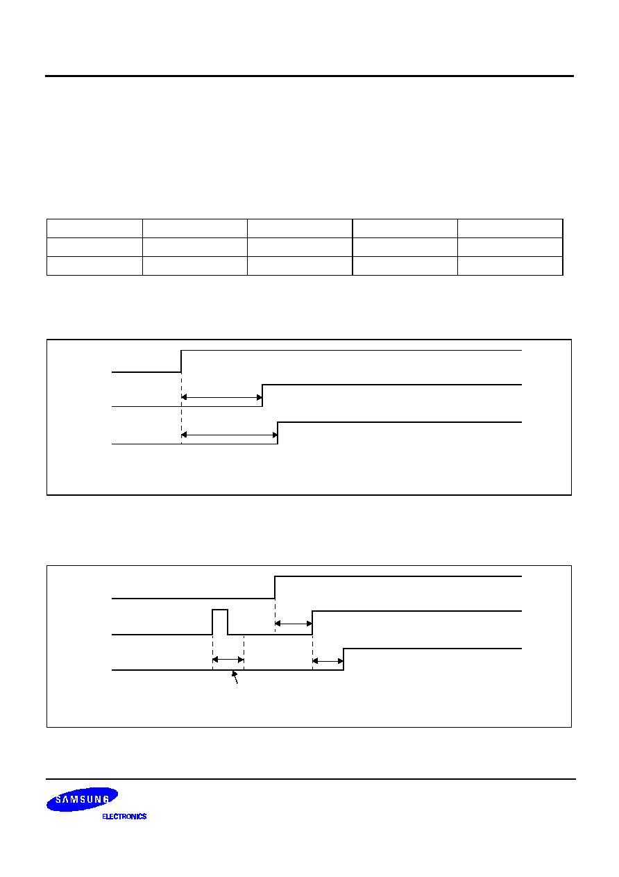
ID DET
ID signal is FM modulated to second carrier (SIF2) with a 2.5kHz FM modulation after AM modulated to 55kHz
PILOT sub-carrier with a 50% AM modulation. ID DET part consists of 3 blocks: that is filter block for extracting pilot
carrier, AM detector block for AM detection of ID signal and digital block for detecting the frequency of provided ID
signal logically. In the filter block, audio signal is removed by HPF and pilot signal is extracted by the automatically
adjusted switch - capacitor BPF (band pass filter) with a center frequency of 55kHz. ID signal is extracted from the
pilot carrier in the AM detector block, then Digital block detects the frequency of ID signal, The ID signal can be
detected in the range shown as follow:
This block
'
s circuit is configured to reduce the blinking of the ID, and consequently has the following characteris-
tics: typ 1 sec and Max 1.5 sec delay when converting from Mono to Stereo, or to Bilingual. 0.3 sec delay when
converting from Stereo or Bilingual to Mono. Therefore, when changing the channels on your TV set, a minimum of
1.5 sec is needed for ID Detect Time.
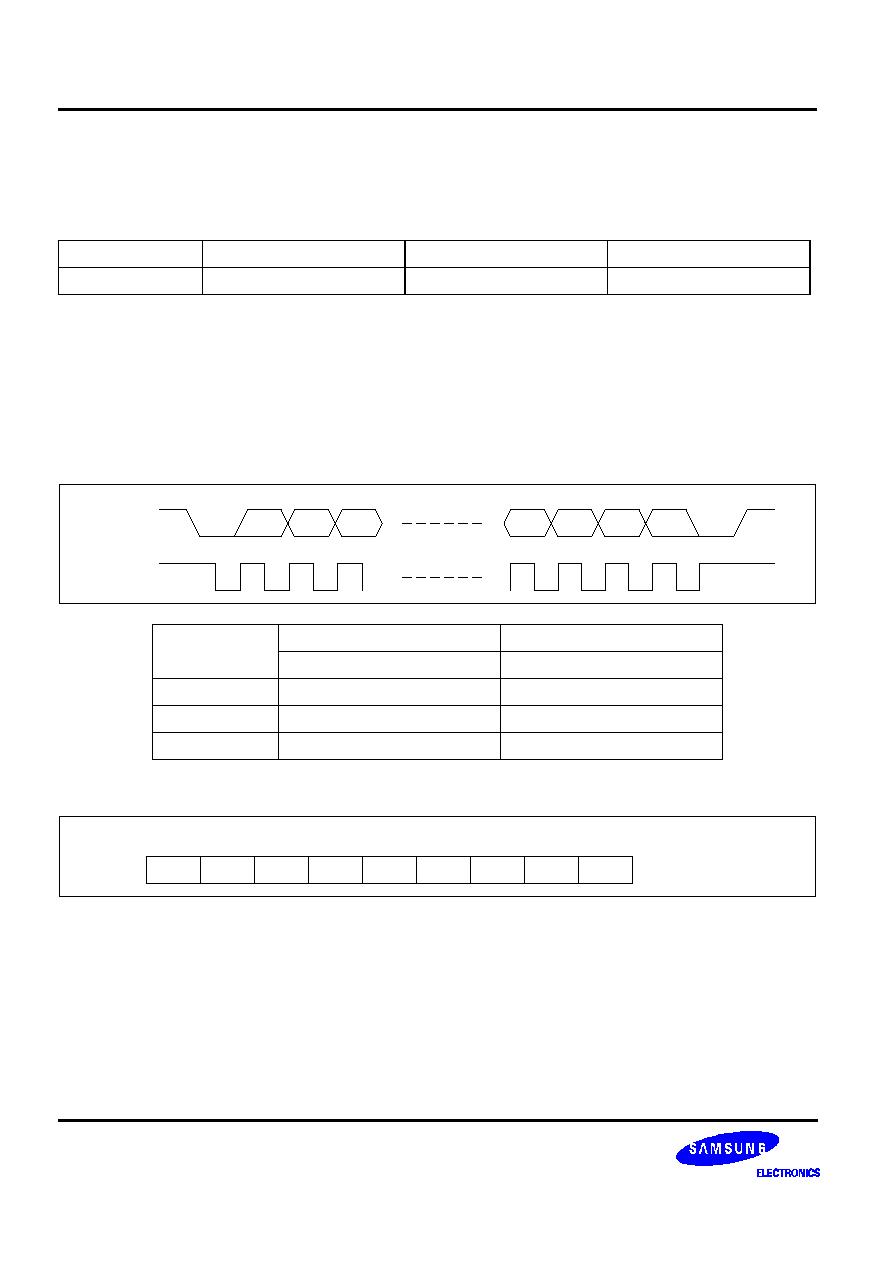
Figure 1. Timing Diagram for Changing Channels from Mono to stereo or Bilingual
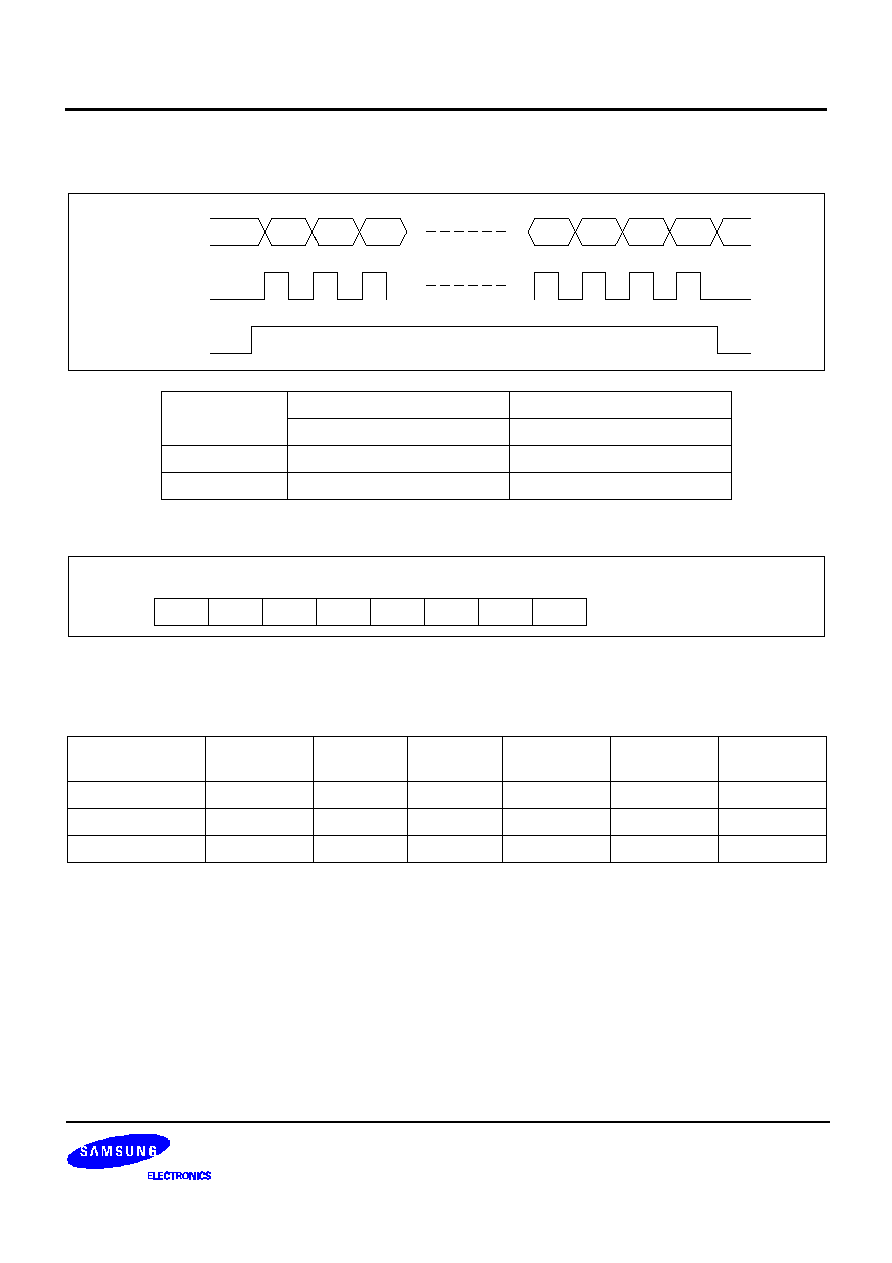
The ID Detect Block of the S1A0688C01 can momentarily malfunction if the signal is weak. Hence, we recommend
that you delay for at least 1 sec at Set MICOM before detecting the ID, if the ID changes at a fixed channel.
Figure 2. Timing Diagram when Channel is Fixed
ID
Low Off
Low On
High On
High Off
Stereo (150 Hz)
125 Hz
140 Hz
160 Hz
176 Hz
Bilingual (276 Hz)
237 Hz
255 Hz
300 Hz
312 Hz
T1
T2
Mono
Mono
Mono
Stereo or Bilingual
Stereo or Bilingual
Stereo or Bilingual
Broadcast
S1A0688C01
Set MICOM
T1: S1A0688C01
'
s ID Detect Time typ 1 sec, Max 1.5 sec
T2: When changing channels, set MICOM
'
s ID Detect Delay Time to a minimum of 1.5 sec.
T1
T3
Mono
Mono
Mono
Stereo or Bilingual
Stereo or Bilingual
Stereo or Bilingual
Broadcast
S1A0688C01
Set MICOM
T1: S1A0688C01
'
s ID Detect Time typ 1 sec, Max 1.5 sec
T3: When the channel is fixed, set MICOM
'
s ID Detect Delay Time to a minimum of 1 sec.
T3
Malfunction Skip
S1A0688C01
TV SOUND MPX FOR TWO CARRIER SYSTEM
14
MICOM
S1A0688C01 is available in DC control, normal microcontroller control, and IIC BUS microcontroller control system,
and it can distinguish the control type automatically by monitoring PIN 22 (EN) status. The relation of control source
type and PIN 22 status is shown as follows.
Protocol of IIC BUS microcontroller control (PIN 22: L)
The S1A0688C01 can be controlled via the 2-line IIC BUS by the microcontroller. The two lines (SDA-serial data.
SCL-serial clock) exchange information between the devices connected to the IIC bus. SDA is bidirectional line
which is connected to a positive supply voltage via a pull up resistor. When the bus is free both lined are HIGH. The
data on the SDA line must be stable during the High-powered of the clock. The HIGH or LOW data can only
change when the clock signal line is LOW. A HIGH -to -LOW transition of the SDA line while SCL is HIGH is
defined as a start condition. A LOW- to -HIGH transition of the SDA line while SCL is HIGH is defined as a stop
condition. The bus receiver will be reset by the reception of a start condition and is considered to be busy after the
start condition. After a stop condition the bus is considered as free again.
Data transmitted to the S1A0688C01 starts with the module address as follows:
IIC Bus
Normal MICOM
DC Control
EN (Pin 22)
always
"
L
"
MICOM strobe
always
"
H
"
1st Byte
1
-
7th bit
Chip select code (1000010B)
8th bit
R/W
9th, 18th, 27th bit
Acknowledge
2nd Byte
10th
-
17th bit
SUB address (function)
3rd Byte
197th
-
26th bit
Data (D1
-
D8)
SDA
SCL
3
2
1
25
26
27
1
0
0
0
0
1
0
R/W
ACK
MSB
LSB
MSB First.
TV SOUND MPX FOR TWO CARRIER SYSTEM
S1A0688C01
15
Protocol of normal microcontroller control (PIN 22: STROBE)
The module address of S1A0688C01 in normal microcontroller control mode is as follows:
.
The maximum STROBE pulse width in normal microcontroller control mode should be under 6.0 msec. If the
STROBE pulse width excess the limit, S1A0688C01 will be changed to DC control mode.
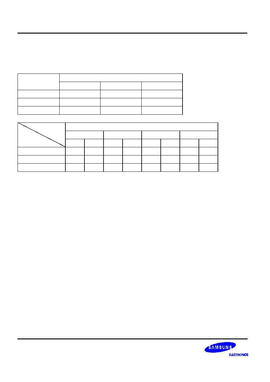
Control Item in Each Control Mode
In each control mode, control items is limited as follows:
NOTES:
1.
PRE-SET: When power is ON, MICOM initials the status of S1A0688C01 to preset status.
(All IC has same preset status data)
2.
PRE-ADJUST SET: When power is ON, MICOM initials the status of S1A0688C01 to pre-measured and stored status.
(Different each IC)
3.
DATA TRANSMISSION: Transmit stored data to MICOM when MICOM requests.
4.
RECEIVE ACKNOWLEDGE: Return acknowledge signal to MICOM after DATA receipt.
1st Byte
1
-
7th bit
Chip select code (1000010B)
8th bit
Not use (don
'
t care)
2nd Type
9th
-
16th bit
Function assignment
3rd Type
17th
-
24th bit
Data (D1
-
D8)
Control
Mode Change
Mute
Preset
Pre-adjust set
Data
Transmission
Receive
Acknowledge
IIC Bus
O
O
O
O
O
O
Normal MICOM
O
O
O
◊
◊
◊
DC Control
◊
◊
◊
◊
◊
◊
SDA
SCL
3
2
1
22
23
24
STROBE
(EN)
1
0
0
0
0
1
0
D
MSB
LSB
MSB First.
S1A0688C01
TV SOUND MPX FOR TWO CARRIER SYSTEM
16
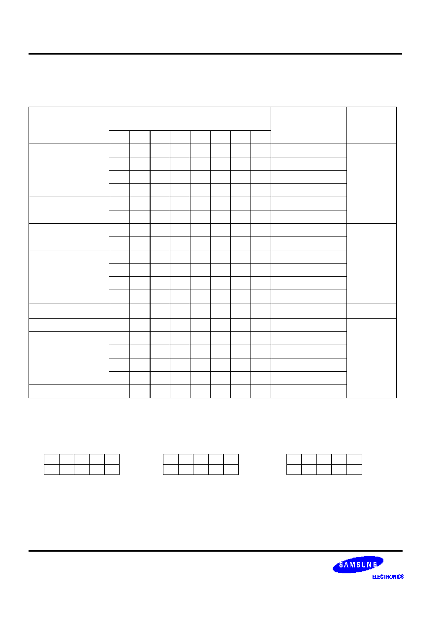
MICOM control map
In IIC BUS mode, SLAVE Address = WRITE: 84H, READ: 85H
In normal MICOM mode, chip select code = 1000010B
NOTES:
1.
MSB first
2.
When power is ON, all latch data are
"
0
"
, S1A0688B is set to MONO OFF, MUTE OFF, SEPARATION
ADJUST DEFAULT (00001XXX).
3.
Separation Adjust Data
SUB ADDRESS
(2nd BYTE)
(MSB<->LSB)
DATA (3rd BYTE)
MSB LSB
FUNCTION
REMARK
D1
D2
D3
D4
D5
D6
D7
D8
000XXXXX
(Mode Control)
0
0
X
X
X
X
X
X
Mono
End user
control
1
0
X
X
X
X
X
X
Stereo
0
1
X
X
X
X
X
X
Bilingual
1
1
X
X
X
X
X
X
Sub
001XXXXX
(Mute Control)
0
X
X
X
X
X
X
X
Mute Off
1
X
X
X
X
X
X
X
Mute
010XXXXX
(Test Mode Control)
0
X
X
X
X
X
X
X
Normal mode
Ic maker
test
1
X
X
X
X
X
X
X
Test mode
011XXXXX
(Free Run Frequency
Control)
0
0
X
X
X
X
X
X
Default
1
0
X
X
X
X
X
X
Frequency down
0
1
X
X
X
X
X
X
Default zap
1
1
X
X
X
X
X
X
Frequency down zap
100XXXXX
D1
D2
D3
D4
D5
X
X
X
Separation adjust
(3)
Set maker
101XXXXX
S1U
S1D
S2U
S2D
X
X
X
X
Pin DC cont.
IC maker
test
110XXXXX
(Test Mode)
0
0
X
X
X
X
X
X
Operating
1
0
X
X
X
X
X
X
Slave zap
0
1
X
X
X
X
X
X
Master zap
1
1
X
X
X
X
X
X
External clock
111XXXXX
X
X
X
X
X
X
X
X
Not use
D1
D2
D3
D4
D5
D1
D2
D3
D4
D5
D1
D2
D3
D4
D5
0
0
0
0
0
(MIN) <---
1
0
0
0
0
(TYP) ---->
1
1
1
1
1
(MAX)
TV SOUND MPX FOR TWO CARRIER SYSTEM
S1A0688C01
17
Control Function Description
∑
MODE CONTROL: Control the MATRIX structure according to broadcast status and end user
'
s setting.
S1A0688C01 has 4 modes (MONO, STEREO, BILINGUAL and SUB)
∑
MUTE CONTROL: When MUTE CONTROL is on, the audio output of S1A0688C01 is off.
∑
SEP. ADJUST: The separation characteristic of S1A0688C01 in STEREO mode can be controlled by IIC BUS.
This option controls S2 FM demodulated output signal level so as to make the separation characteristic in best
status.
∑
TEST MODE: IC makers test item.
DC Control Map (PIN22: H)
READ Mode in IIC BUS MICOM Control Mode
S1A0688C01 can transmit the data which is registered inside IC to the MICOM in IIC BUS control system.
If the 8th bit of module address is
`
H
'
, it means MICOM requests the data stored in the IC and S1A0688C01 enter
data transmission mode. During the read mode, S1A0688C01 ignores the data the data of 2nd type (SUB address)
and transmits the internal data within the period of 3rd byte. The SDA line of MICOM should be maintain H to
accept transmitted data from IC. The format of read data is as follows.no
DC (Logic) Input
Function
SCL
SDA
0
0
Mono
1
0
Stereo
0
1
Bilingual
1
1
Sub
Bit of 3rd Byte
1
2
3
4
Read Mode
5
6
7
8
Transmit Data
BI
ST
BI
ST
ZC
ZC
0
1
0
0
1
1
Mono
Option for IC maker
(ZC: IC test option)
1
0
0
1
Bilingual
0
1
1
0
Stereo
Others
Transmission error
S1A0688C01
TV SOUND MPX FOR TWO CARRIER SYSTEM
18
Others
In IIC BUS control system, if the SLAVE address is correct, the acknowledge signal will be generated by
S1A0688C01 no matter the sub address is right or wrong, When sub address is wrong IC will do nothing.
NOTES:
1.
The characteristic of SIF Filter should be suitable to MPX sound system.
We suggest to use MURATA Co. products: SFSH4.5MCB and SFSH4.72MCB.
2.
If you need to use two chip in one set (e.g. TVCR), You should separate the chips by select pin 28 voltage.
When it is high or open, Write =84H, Read = 85H.
When pin 28 is connected to ground, Write =86H, Read = 87H.
3.
Program control method:
1. Under window 95 environment, extract kb22688b.zip
2. Install: setup.exe
3. Run kb22688b.exe
4.
PC parallel port pin description:
PIN
1
2
3
19
SIGNAL
SDA
SCL
EN
GND
TV SOUND MPX FOR TWO CARRIER SYSTEM
S1A0688C01
19
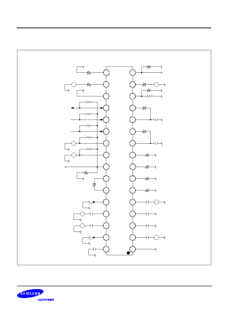
TEST CIRCUIT
R-OUT
L- OUT
VCC
S1A0688C01
1
2
3
4
7
28
27
26
25
8
5
6
30
29
32
31
9
10
11
12
15
14
13
16
20
19
18
17
22
21
24
23
0.047
µ
F
0.047
µ
F
1
µ
F
1
µ
F
10
µ
F
10
µ
F
4.7
µ
F
0.039
µ
F
0.039
µ
F
10
µ
F
1M
4.7
µ
F
100
µ
F
4.7
µ
F
10
µ
F
SDA
SCL
EN
ST
TCLK
1
µ
F
10
µ
F
0.1
µ
F
4.7
µ
F
S
S
0.047
µ
F
0.047
µ
F
SIF1
SIF2
M
M
M
BI
M
S
M
47k
47k
47k
47k
47k
0.1
µ
F
0.1
µ
F
RCM
S2
S1
VDD
S1A0688C01
TV SOUND MPX FOR TWO CARRIER SYSTEM
20
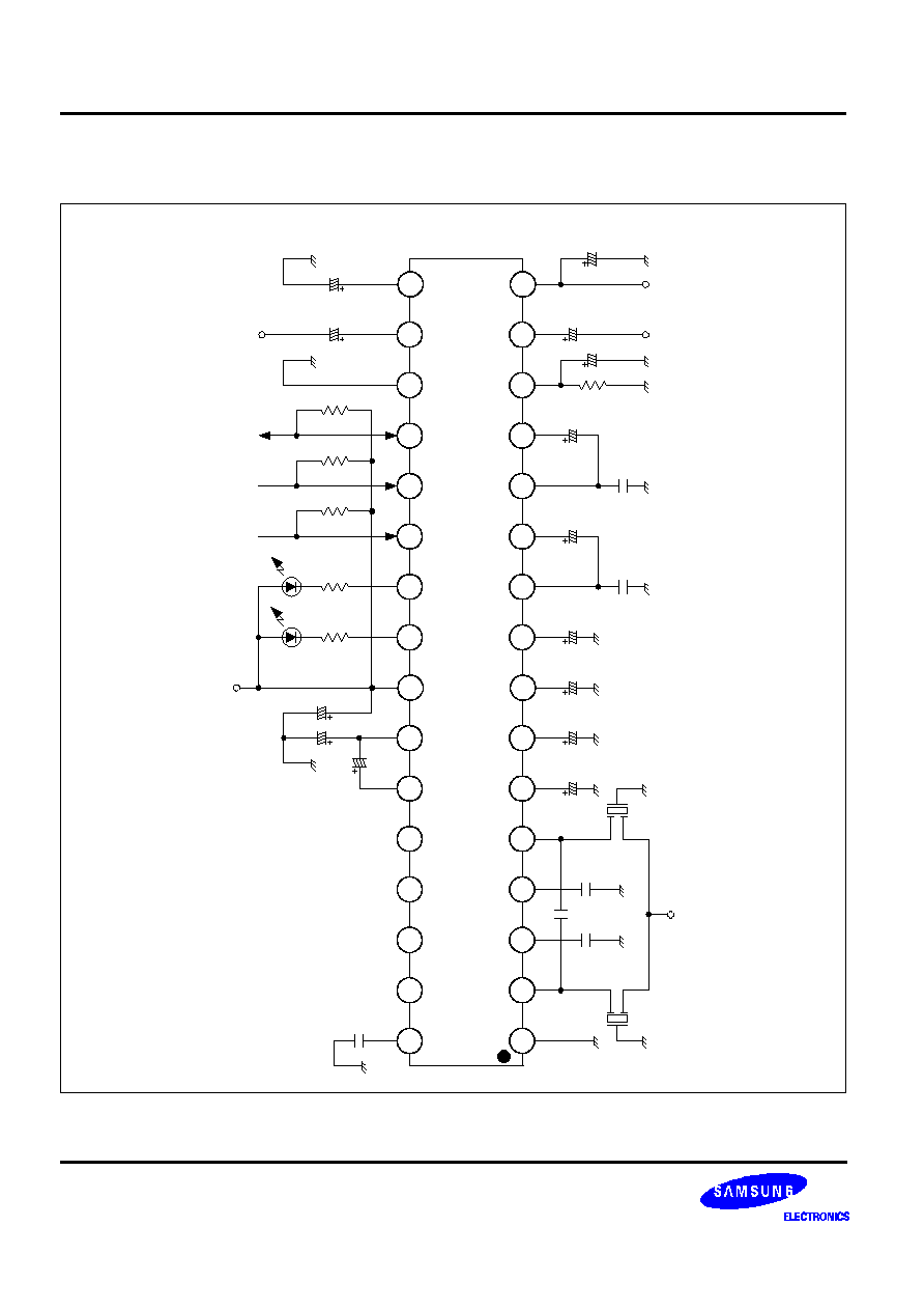
APPLICATION CIRCUIT
R-OUT
L- OUT
4.72MHz
3pF
VCC
S1A0688C01
1
2
3
4
7
28
27
26
25
8
5
6
30
29
32
31
9
10
11
12
15
14
13
16
20
19
18
17
22
21
24
23
0.047
µ
F
0.047
µ
F
4.5MHz
1
µ
F
1
µ
F
10
µ
F
10
µ
F
4.7
µ
F
0.039
µ
F
0.039
µ
F
10
µ
F
1M
4.7
µ
F
100
µ
F
4.7
µ
F
10
µ
F
SDA
SCL
EN
ST
N.C
VDD
1
µ
F
100
µ
F
1
µ
F
0.1
µ
F
N.C
N.C
N.C
4.7
µ
F
47k
47k
47k
470
470