DUAL LOW NOISE EQ AMP
S1A2221A01
1
INTRODUCTION
The S1A2221A01 is a monolithic integrated circuit for car ste-
reos,which possesses 2-channel low noise amplifiers and a
regulated power supply.
FEATURES
∑
Suitable for a car stereo
∑
Low noise amplifier
∑
Voltage regulator included
∑
Good ripple rejection
∑
High channel separation (65dB Typ)
∑
Minimum number of external parts required
ORDERING INFORMATION
BLOCK DIAGRAM
Device
Package
Operating Temperature
S1A2221A01-I0U0
8
-
SlP
-
20
∞
C -- +70
∞
C
8
-
SIP
1
2
3
4
5
6
7
8
+
-
AMP1
VOLTAGE
REGULATOR
+
-
AMP1
INPUT1
NF1
OUTPUT1
V
CC
OUTPUT2
NF2
INPUT2
GND

S1A2221A01
DUAL LOW NOISE EQ AMP
2
ABSOLUTE MAXIMUM RATINGS (Ta = 25
∞
C)
ELECTRICAL CHARACTERISTICS
(T = 25
∞
C, V
CC
= 12V, R
L
= 10K, f = 1kHz, NAB, unless otherwise specified)
Characteristic
Symbol
Value
Unit
Supply Voltage
V
CC
18
V
Power Dissipation
P
O
200
mW
Operating Temperature
T
OPR
-
20 -- +70
∞
C
Storage Temperature
T
STG
-
40 -- +125
∞
C
Characteristic
Symbol
Test Conditions
Min.
Typ.
Max.
Unit
Quiescent Circuit Current
I
CCQ
V
I
= 0
-
6.0
9.0
mA
Open Loop Voltage Gain
G
VO
-
65
80
-
dB
Closed Loop Voltage Gain
G
VE
V
O
= 0.5 V
33
35
37
dB
Output Voltage
V
O
THD = 1%
0.6
1.0
-
V
Total Harmonic Distortion
THD
V
O
= 0.5 V
-
0.1
0.3
%
Input Resistance
R
I
-
-
150
-
K
Equivalent Input Noise Voltage
V
NI
R
G
= 2.2k
BW (
-
3dB) =15Hz
-
30kHz
-
1.0
2.0
µ
V
Cross Talk
CT
R
G
= 2.2k
50
65
-
dB

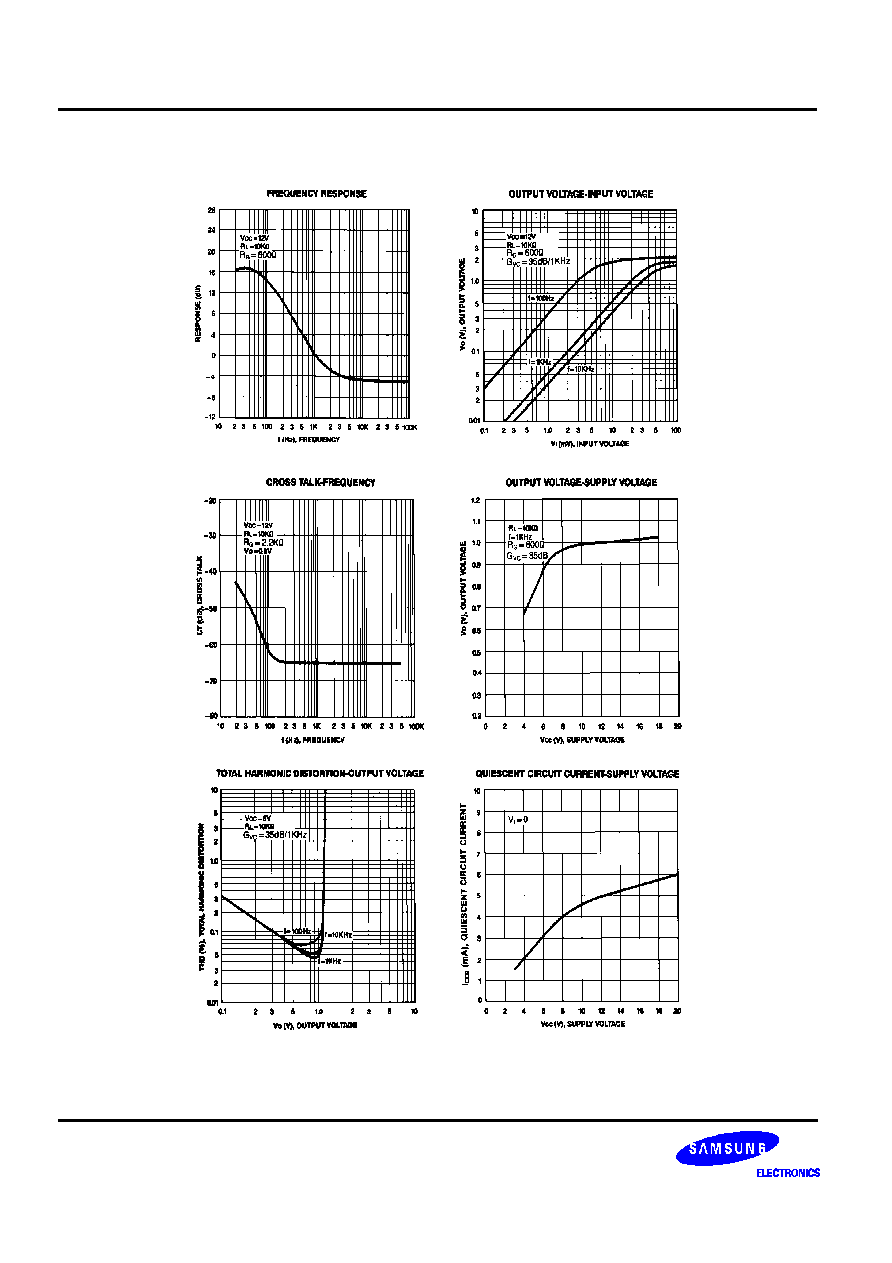
DUAL LOW NOISE EQ AMP
S1A2221A01
5
APPLICATION INFORMATION
External Components (Refer to test circuits)
C
1
(C
10
): Noise filter
These capacitors prevent radio interference in strong electric fields. The recommended value is 1000 pF.
C
2
(C
8
):Input coupling capacitor
The recommended value is 10
µ
F. If made too small, the low frequency characteristics will change for the
worse, but too large a value will increase the rising time when power is applied.
C
1
(C
9
):Negative feedback capacitor
The lower cut-off frequency depends on the value of these capacitors and is determined as follows:
f
L
: Low cut-off frequency
If the value of these capacitors is made larger, the starting time of the amplifier is delayed further.
C
5
(C
6
): Output coupling capacitor
The recommended value is 10
µ
F.
R
2
, R
3
, C
7
(R
4
, R
5
, C
4
): Equalizer network
The time constants of standard NAB characteristic are as follows.
R
1
(R
6
): Feedback component
The closed loop gain is determined approximately by the following relationship.
Choose R
2
, R
3
, (DC resistance of NAB element) as 100 K approximately.
Tape speed
9.5 cm/sec
4.75 cm/sec
T2
T1
C
7
(R
2
+ R
3
)
R
2
, C
7
3180
µ
sec
90
µ
sec
1590
µ
sec
120
µ
sec
C
3
(C
8
) =
1
2
f
L
∑
R1
+
47
µ
R
1
R
2
R
3
C
7
GVC = 20 log (dB)
Z = R
2
+ R
3
//C
7
Z + R
1
R
1