
DEFLECTION PROCESSOR FOR MULTISYNC MONITORS
S1D2147A01
0
DEFLECTION PROCESSOR
The S1D2147A01is a monolithic integrated circuit assembled
in a 42 pins shrunk dual in line plastic package.
The goal of this IC is to control all the functions related to the
horizontal and vertical deflection in multimodes or multisync
monitors.
FUNCTIONS
∑ Positive or Negative sync polarities
∑ Auto-sync horizontal processing
∑ H-PLL lock/unlock identification
∑ Auto-sync Vertical processing
∑ East/West signal processing block
∑ B+ controller
∑ Safety blanking output
FEATURES
(HORIZONTAL)
∑ Dual Pll concept
∑ Self-adaptative (30 to 70kHz)
∑ X-ray protection input
∑ DC adjustable duty-cycle
∑ Internal 1st
PLL lock/unlock information
∑ Wide range DC controlled H-position
∑ ON/OFF switch (for PWR management)
∑ Two H-drive polarities
(VERTICAL)
∑ Vertical ramp generator
∑ 50 to 120Hz AGC Loop
∑ DC controlled V-amp, V-pos, S-amp & S-centring
∑ ON/OFF Switch
(B+ REGULATOR)
∑ Internal PWM generator for B+ current mode
step-up conveter
∑ DC adjustable B+ voltage
∑ Output pulse synchronised on horizontal frequency
∑ Internal MAX current limitation
42-SDIP-600
ORDERING INFORMATION
Device
Package
Operation Temperature
S1D2147A01-A0B0
42-SDIP
0
∞
C -- 70
∞
C
(GENERAL)
∑ Accept Positive or Negative Horizontal &
Vertical sync polarities
∑ Separate H & V TTL input
∑ Safety blanking output
(E
WPCC
)
∑ Vertical parabola generator with DC
∑ controlled keystone & amplitude
S1D2147A01 DEFLECTION PROCESSOR FOR MULTISYNC MONITORS
1
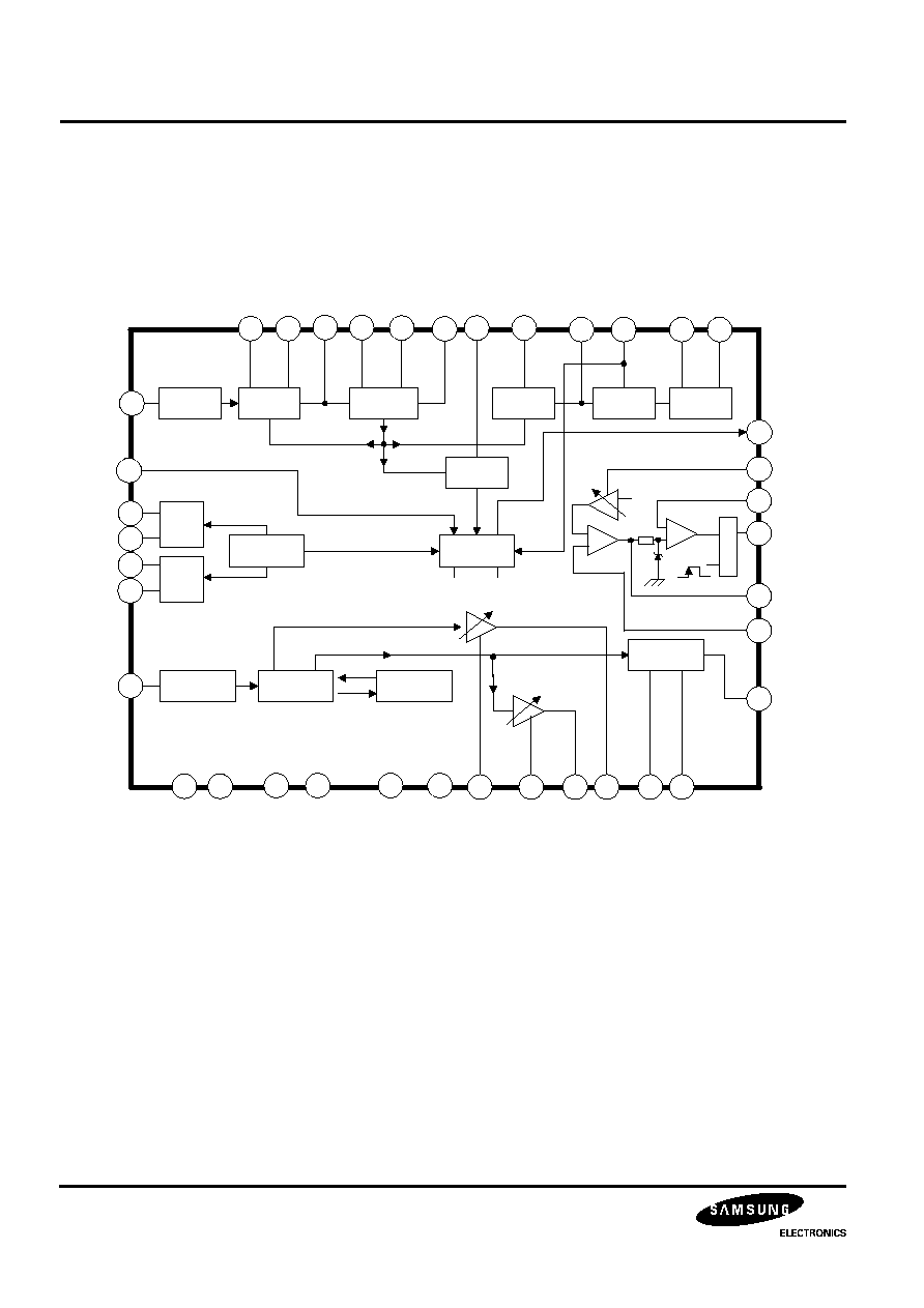
BLOCK DIAGRAM
SBLKOUT
4
16
17
34
22
42
39
23
41
19
+
-
INPUT
INTERFACE
1st PHASE
COMP
VCO
2nd PHASE
COMP
LOCK
DETECT
SAFETY
PROCESSOR
PHASE
SHAPER
OUTPUT
BUTTER
35
15
12
11
10
14
13
3
1
2
20
21
-
+
R
S
40
36
BANDGAP
EA
H-VREF
5
24
26
V-VREF
INPUT
INTERFACE
VERTICAL
OSCILLATOR
S
CORRECTION
PARABOLA
GENERATOR
28
29
27
25
18
33
31
30
32
38
37
EW-AMP
GND
VCC
VCAP
VAGCCAP
VS-CENT
VS-AMP
V-POS
V-AMP
VOUT
DCOUT
KEYST
B+ADJ
I
B+OUT
COMP
REGIN
E/WOUT
HSYNC
XRAY-IN
HREF
HGND
VGND
VREF
VSYNC
PLL1NHIB
H-POS
PLL1F
R0
C0
FH-MIN
HLOCK-CAP
HFLY
PLL2C
H-DUTY
H-OUTEM
H-OUTCOL
V
VCC
OUTPUT
INHIBITION
SENSE
REF
V
DEFLECTION PROCESSOR FOR MULTISYNC MONITORS
S1D2147A01
2
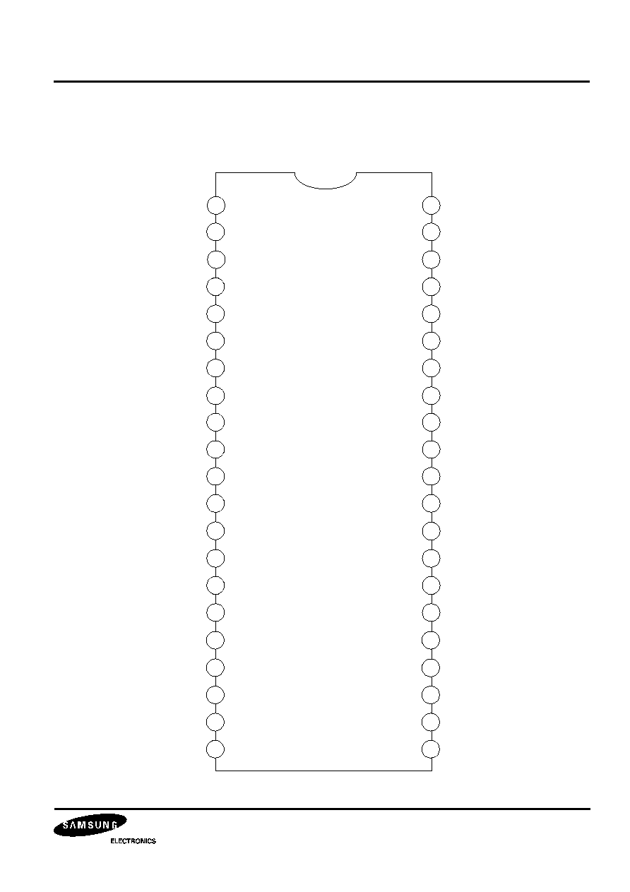
PIN CONFIGURATIONS
V-AMP
COMP
REGIN
HREF
NC
NC
NC
HGND
PLL1-INHIB
E/WOUT
VS-CENT
VSYNC
B+ ADJ
9
3
2
1
6
5
8
7
37
31
41
40
35
36
10
29
39
34
VOUT
FH-MIN
PLL1F
4
14
12
38
NC
HFLY
H-DUTY
PLL2C
13
C0
HLOCK-CAP
11
R0
30
KEYST
I-SENSE
V-POS
42
32
V-DCOUT
33
S1D2147
15
16
28
27
H-POS
XRAY-IN
VS-AMP
VCAP
VREF
VGND
26
24
VAGCCAP
GND
HSYNC
19
17
18
VCC
25
20
21
23
22
H-OUTEM
H-OUTCOL
SBLK-OUT
B+ OUT
E/W-AMP

S1D2147A01 DEFLECTION PROCESSOR FOR MULTISYNC MONITORS
3
PIN DESCRIPTION
Table 1. Pin Description
Pin No
Pin Name
Description
1
PLL2C
Second PLL Loop Filter
2
H-DUTY
DC Control of Horizontal Drive Output Pulse Duty-cycle.
If this pin grounded, the horizontal and vertical outputs are inhibited. By connecting a
capacitor on the this pin a soft-start function may be realized on h-drive output.
3
H-FLY
Horizontal Flyback Input (Positive Polarity)
4
H-GND
Horizontal section ground. Must be connected only to components related to H
blocks.
5
H-REF
Horizontal section reference voltage. Must be filtered by capacitor to pin 4.
6
NC
7
NC
8
NC
9
NC
10
C0
Horizontal Oscillator Capacitor. To be connected to pin 4.
11
R0
Horizontal Oscillator Resistor. To be connected to pin 4.
12
PLL1F
First PLL Loop filter. To be connected to pin 4.
13
HLOCK-CAP
First PLL Lock/Unlock Time Constant Capacitor. Capacitor filtering the freqency
change detected on pin 13. When frequency is changing, a blanking pulse is
generated on pin 23, the duration of this pulse is proportionnal to the capacitor on
pin 13. To be connected to pin 4.
14
FH-MIN
DC Control for free running frequency setting. Comming from DAC output or DC
voltage generated by a resistor bridge connected between pin 5 and 4.
15
H-POS
DC Control for Horizontal Centering
16
XRAY-IN
X-RAY Protection input (with Internal latch function)
17
H-SYNC
TTL Horizontal Sync Input
18
Vcc
Supply Voltage (12V Typical)
19
GND
Ground
20
H-OUTEM
Horizontal Drive Output (emiter of internal transistor)
21
H-OUTCOL
Horizontal Drive Output (open collector of internal transistor)
22
B+OUT
B+ PWM Regulator output
23
SBLK
OUT
Safety Blanking output. Activated during frequency changes, when X-RAY input is
triggered or when VS is too low.
24
VGND
Vertical Section Signal Ground
25
VAGCCAP
Memory Capacitor for Automatic Gain Control Loop in Vertical Ramp Generator
26
V
REF
Vertical Section Reference Voltage

DEFLECTION PROCESSOR FOR MULTISYNC MONITORS
S1D2147A01
4
27
VCAP
Vertical Sawtooth Generator Capacitor
28
VS-AMP
DC Control of Vertical S-Shape Amplitude
29
VS-CENT
DC Control of Vertical S-Centering
30
V-OUT
Vertical Ramp Output (with frequency independant amplitude and S-Correction)
31
V-AMP
DC Control of Vertical Amplitude Adjustment
32
VDCOUT
Vertical Position Reference Voltage Output Temperature matched with V-AMP
output
33
V-POS
DC Control of Vertical Position Adjustment
34
V-SYNC
Vertical TTL Sync Input
35
PLL1INHIB
TTL Input for PLL1 Output Current Inhibition (To be used in case of comp sync input
signal)
36
E/WOUT
East/West Pincushion Correction Parabola Output
37
E/W-AMP
DC Control East/West Pincushion Correction Amplitude
38
KEYST
DC Control of Keystone Correction
39
B+ADJ
DC Control of B+ Adjustment
40
REGIN
Regulation Input of B+ Control Loop
41
COMP
B+ Error Amplifier Output for Frequency Compensation and Gain Setting
42
I
SENSE
Sensing of External B+ Switching Transistor Emitter Current
Table 1. Pin Description (Continued)
Pin No
Pin Name
Description

S1D2147A01 DEFLECTION PROCESSOR FOR MULTISYNC MONITORS
5
ABSOLUTE MAXIMUM RATINGS
THERMAL CHARACTERISTICS
HORIZONTAL SECTION
OPERATING CONDITIONS
NO
Item
Symbol
Spec
Unit
1
Supply Voltage (Pin 18)
V
CC
13.5
V
2
Maximum Voltage on Pins 2, 14,15, 28, 29, 31, 33, 37, 38, 39
Pin 3
Pins 17, 34
Pin 40
Pin 42
Pin 16
V
IN
8
1.8
6
8
8
6
V
3
ESD Succeptibility
Human Body Model, 100pF Discharge through 1.5k
EIAJ Norm, 200pF Discharge through 0
VESD
2
300
kV
V
4
Storage Temperature
T
stg
-40, +150
∞
C
5
Maximum Operating Junction Temperature
T
j
150
∞
C
6
Operating Temperature
T
opr
0, +70
∞
C
NO
Item
Symbol
Spec
Unit
1
Junction-Ambient Thermal Resistance
ja
65
∞
C/W
Parameter
Symbol
Conditions
Min
Typ
Max
Unit
VCO
Oscillator Resistor Min Value (Pin 11)
R0min
6
k
Oscillator Capacitor Min Value (Pin 10)
C0min
390
pF
Maximum Oscillator Frequency
Fmax
70
kHz
Horizontal Sync Input Voltage (Pin 17)
HsVR
0
5.5
V
INPUT SECTION
Minimum Input Pulses Duration (Pin 17)
MinD
1
µ
S
Maximum Input Signal Duty Cycle (Pin 17)
Mduty
25
%
OUTPUT SECTION
Maximum Input Peak Current (Pin 3)
I3m
2
mA
Horizontal Drive Output Max Current
Pin 20
Pin 21
HOI1
HOI2
Sourced current
Sink current
20
20
mA
mA
DC CONTROL VOLTAGE

DEFLECTION PROCESSOR FOR MULTISYNC MONITORS
S1D2147A01
6
DC Voltage Range on DC Controls (Pins 2-14-15)
DCadj
V
REF-H
= 8V
2
6
V
Parameter
Symbol
Conditions
Min
Typ
Max
Unit

S1D2147A01 DEFLECTION PROCESSOR FOR MULTISYNC MONITORS
7
ELECTRICAL CHARACTERISTICS
(Vcc = 12 V, Tamb = 25
∞
C)
Table 2. Horizontal Section Electrical Characteristics
Parameter
Symbol
Conditions
Min
Typ
Max
Unit
SUPPLY AND REFERENCE VOLTAGES
Supply Voltage (Pin 18)
V
CC
10.8
12
13.2
V
Supply Current (Pin 18)
I
CC
See Figure 1
40
60
mA
Reference Voltage for Horizontal
Section (Pin 5)
V
REF-H
7.4
8
8.6
V
Max Sourced Current on V
REF-H
(Pin 5)
I
REF-H
2
mA
Reference Voltage for Vertical
Section (Pin 26)
V
REF-V
7.4
8
8.6
V
Max Sourced Current on V
REF-V
(Pin 26)
I
REF-V
2
mA
INPUT SECTION/PLL1
Horizontal Input Threshold Voltage
(Pin 17)
V
INTH
Low level voltage
High level voltage
2
0.8
V
VCO Control Voltage (Pin 12)
V
VCO
V
REF-H
= 8V
1.6 to 6.2
V
VCO Gain, dF/dV (Pin 12)
V
COG
R0 = 6.49k
,
C0 = 680pF
15
kHz/V
Horizontal Phase Adjustment
(Pin 15)
Hph
% of Horizontal period
±
10
%
Free running frequency
adjustment (pin 14)
FFadj
Without H-sync signal
±
20
%
PLL1 Capture Range
Fh Min
Fh Max
CR
See conditions on Figure 1
70
28
kHz
kHz
PLL 1 Inhibition (Pin 35)
PLL ON
PLL OFF
PLLinh
V
35
V
35
2
0.8
V
V
SECOND PLL AND HORIZONTAL OUTPUT SECTION
Flyback Horizontal Threshold
Voltage (Pin 3)
FBth
0.65
0.75
V
Horizontal Jitter
Hjit
150
ppm
Horizontal Drive Output Duty-cycle
(Pin 20 or 21)
Minimum
Maximum
HDmin HDmax
V
2
= 2V
V
2
= 2V
45
30
50
35
%
%
Horizontal Drive Low Level Output
Voltage
HDvd
Pin 20 to GND,
V
21
-V
20
, I
OUT
= 20mA
1.1
1.7
V

DEFLECTION PROCESSOR FOR MULTISYNC MONITORS
S1D2147A01
8
VERTICAL SECTION
OPERATING CONDITIONS
ELECTRICAL CHARACTERISTICS
(VCC = 12V, Tamb = 25
∞
C)
Horizontal Drive High Level Output
Voltage (output on Pin 20)
HDem
Pin 21 to V
CC
,
I
OUT
= 20mA
9.5
10
V
X-RAY Protection Input Threshold
Voltage (Pin 16)
XRAYth
1.6
1.8
V
Maximum Output Current on Safety
Blanking Output
ISblkO
I
23
10
mA
Low-Level Voltage on Safety
Blanking output
VSblkO
V
23
with I
23
= 10mA
0.25
0.5
V
Internal Clamping Voltage on 2nd
PLL Loop Filter Output (Pin 1)
Vphi2
Vmin
Vmax
1.6
3.2
V
Pin2 Threshold Voltage to Stop
H-out, V-out
B+out and to Activate S-BLK
(OFF Mode when V
2
< V
OFF
)
V
OFF
V
2
1
V
Parameter
Symbol
Conditions
Min
Typ
Max
Unit
Vertical Sync Input Voltage (Pin 34)
VSVR
0
5.5
V
Table 3. Vertical Section Electrical Characteristics
Parameter
Symbol
Conditions
Min
Typ
Max
Unit
Pin 23-28-29 bias current
(Currnt sourced by PNP base)
IBIASP
For V23-28-29 = 2V
2
∞
C
Pin 31 bias Current
(Current sunk by PNP base)
IBIASN
For V31 = 6V
0.5
∞
C
Vertical sync input threshold voltage
VSth
Pin 34; High-level
Low -level
2
0.8
V
V
Vertical sync input bias current
(Current sourced by PNP base)
VSBI
V34 = 0.8V
1
µ
A
Voltage at ramp bottom point
VRB
On Pin 27
2/8
VREF-V
Voltage at ramp top point (with sync)
VRT
On Pin 27
5/8
VREF-V
Voltage at ramp top point (without sync)
VRTF
On Pin 27
VRT-0.1
V
Table 2. Horizontal Section Electrical Characteristics (Continued)
Parameter
Symbol
Conditions
Min
Typ
Max
Unit

S1D2147A01 DEFLECTION PROCESSOR FOR MULTISYNC MONITORS
9
Output current range on pin 27 during
ramp charging time. Current to charge
capacitor between pin 27 and ground
IR27
V28 = 2V
(2)
,
2V < V27 < 5V
Min current
Max current
100
15
135
20
µ
A
µ
A
Minimum Vertical sync pulse width
VSW
Pin 34
5
µ
S
Vertical sync input maximum duty-cycle
VSmDut Pin 34
15
%
Vertical Sawtooth discharge time duration
VSTD
On pin 27, with 150nF
cap
85
µ
S
Vertical Free running frequency ( V28 = 2V )
VFRF
Measured on pin 27
Cosc (pin 27) = 150nF
100
Hz
AUTO-SYNC frequency see
(3)
ASFR
With C27 = 150nF
±
5%
50
120
Hz
Ramp Amplitude Thermal Drift
RATD
On pin 30 see
(1)
(0
∞
C < Tamp < 70
∞
C )
100
ppm/
∞
C
Ramp Amplitude Drift Versus Frquency
RAFD
V31 = 6V, C27 = 150nF
50Hz < F < 120Hz
200
ppm/
Hz
Ramp Linearity on Pin 27 127 / I27
RIin
V28 = 2V, V25 = X =
4.3V
2.5V < V27 < 4.5V
0.5
%
Minimum Load on Pin 25 for less than 1%
Vertical Amplitude Drift
RIoad
50
k
Vertical Position Adjustment Votlage on pin 32
Vpos
V33 = 2V
V33 = 4V
V33 = 6V
3.65
3.2
3.5
3.8
3.3
V
V
V
Max Current on Vertical Position Control output
(pin32)
IVPOS
±
2
mA
Vertical Output Votlage (on pin 30)
(peak to peak voltage on pin 30)
Vor
V31 = 2V
V31 = 4V
V31 = 6V
3.75
2
3
4
2.2
V
V
V
DC Votlage on Vertical Output (pin 30)
VOUTDC See
(4)
7/16
VREF-V
Vertical output maximum output current
V0I
On Pin 30
±
5
mA
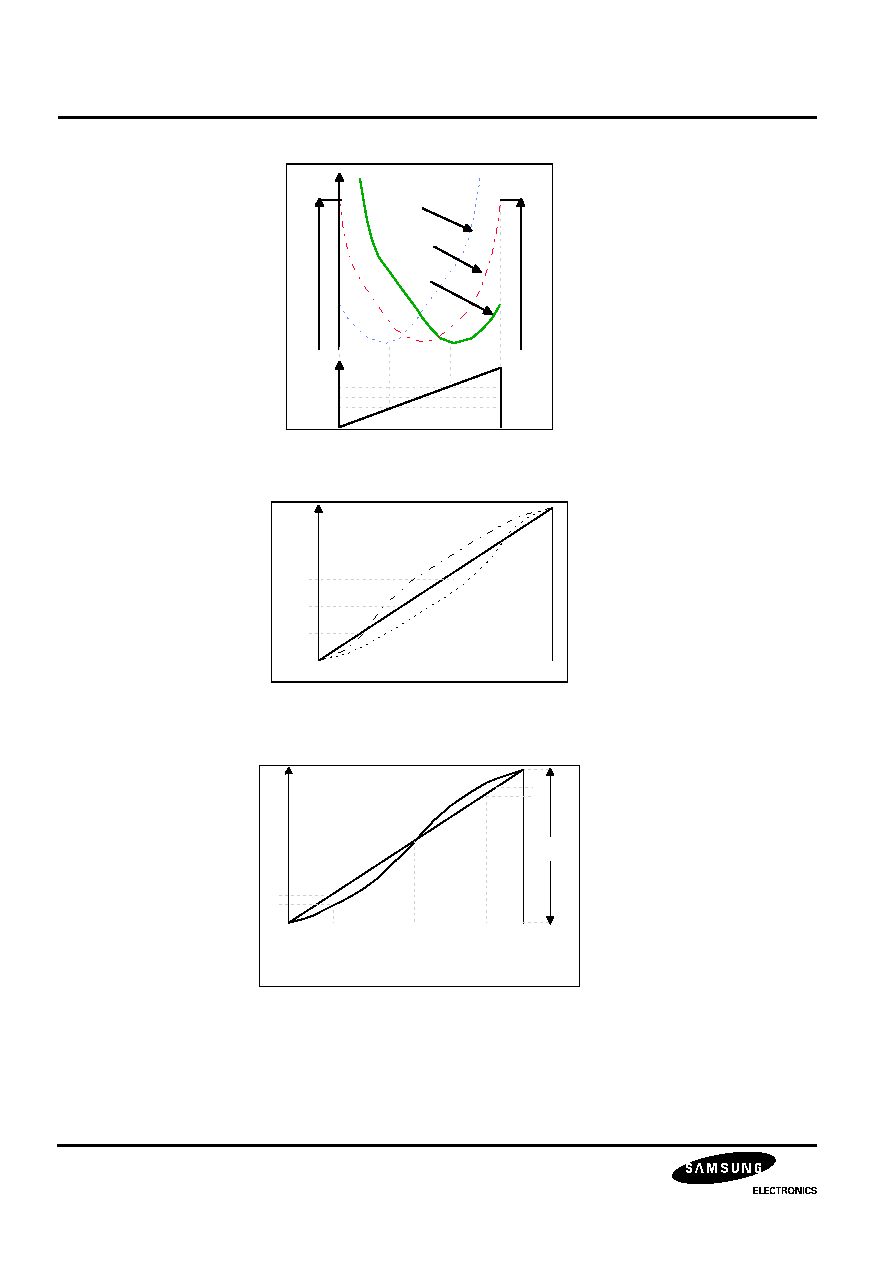
Max vertical S-Correction Amplifitude
(V28 = 2V inhibits S-CORR; V28 = 6V gives
maximum S-CORR) (see figure 3)
dVS
V/V30pp at T/4
V/V30pp at 3T/4
-4
+4
%
%
C-Correction adjustment range voltage on
pin 27 for maximum slope on the ramp
(with S-Correstion ) (see figure 4)
Ccorr
V29 = 2V
V29 = 4V
V29 = 6V
3
3.5
4
V
V
V
Table 3. Vertical Section Electrical Characteristics (Continued)
Parameter
Symbol
Conditions
Min
Typ
Max
Unit

DEFLECTION PROCESSOR FOR MULTISYNC MONITORS
S1D2147A01
10
B+ SECTION
OPERATING CONDITIONS
ELECTRICAL CHARACTERISTICS
(V
CC
= 12V, Tamb = 25
∞
C)
EAST/WEST PARABOLA GENERATOR
ELECTRICAL CHARACTERISTICS
(VCC = 12V, Tamb = 25
∞
C)
Parameter
Symbol
Conditions
Min
Typ
Max
Unit
Maximum Error Amplifier Output
Current
EAOI
Source by pin 14
Sunk by pin 41
0.5
2
mA
mA
Minimum Feedback Resistor
FeedRes Resistor between pins 40 and 41
5
k
Table 4. B+ Section Electrical Characteristics
Parameter
Symbol
Conditions
Min
Typ
Max
Unit
Error Amplifier Open loop gain
OLG
At low frequency
see
(
1
)
85
dB
Unity gain bandwidth
UGBW
see
(1)
6
MHz
Regulation input bias current
IRI
Current sourced by
pin 40 (PNP base)
0.2
µ
A
Maximum guaranted error amplifier
output current
EAOI
Current sourced by pin 41
Current sink by pin 41
0.5
2
mA
mA
Current Sense Input Voltage Gain
CSG
Pin 42
3
Max Current Sense Input Threshold
Votlage
MCEth
Pin 42
1.2
V
Current Sense Input Bias Current
ISI
Current sunk by pin 42
(NPN base)
1
µ
A
Maximum External Power Transistor
on Time
Tonmax
% of H-period
@ f0 = 27kHz
75
%
B+ Output Low Level Saturation
voltage
B+OSV
V
22
with I
22
= 10mA
0.25
V
Internal Reference voltage
IVref
On error amp (+) input for V
39
= 4V
4.9
V
Internal Reference Voltage Adjustment
V
RERADJ
2V < V39 < 6V
±
14
%
Table 5. East/West Parabola Generator Electrical Characteristics
Parameter
Symbol
Conditions
Min
Typ
Max
Unit
Parabola symetry adjustment capability
(for Keystone adjustment; with pin 38)
Vsym
See figure 2; Internal voltage
V38 = 2V
V38 = 4V
V38 = 6V
3.2
3.5
3.8
V

S1D2147A01 DEFLECTION PROCESSOR FOR MULTISYNC MONITORS
11
NOTES:
1.
These parameters are not tested on each unit. They are measured during our internal qualification procedure
which includes characterization on batches comming from comers of our processes and also temperature
characterization.
2 . When 2V are applied on pin 28 (Vertical S-Correction control ), then the S-Correction is inhibited, consequently the
sawtooth have a linear shape.
3.
It is the frequency range for which the VERTICAL OSCILLATOR will automatically synchorize, using a single
capacitor value on Pin 27 and with a constant ramp amplitude.
4.
Typically 3.5V for vertical reference voltage typical value (8V).
Keystone adjustment capability
B/A ratio
A/B ratio
Kadj
See figure 2; V37 = 4V
V38 = 2V
V38 = 6V
2.3
2.0
Parabola amplitude adjustment capability
Maximum amplitude on pin 36
Maximum ratio between max and min
Paramp
V38 = 4.3V, V28 = 2V
V37 = 2V
2V < V37 < 6V
3.3
2.4
3.8
3
4.3
V
Table 5. East/West Parabola Generator Electrical Characteristics (Continued)
Parameter
Symbol
Conditions
Min
Typ
Max
Unit

DEFLECTION PROCESSOR FOR MULTISYNC MONITORS
S1D2147A01
12
APPLICATION CIRCUIT
Figure 1. Application Circuit
V-AMP
COMP
REGIN
HREF
S4
S2
S3
HGND
PLL1-INHIB
E/WOUT
VS-CENT
VSYNC
B+ ADJ
VOUT
FH-MIN
PLL1F
S1
HFLY
H-DUTY
PLL2C
C0
HLOCK-CAP
R0
KEYST
I-SENSE
V-POS
V-DCOUT
H-POS
XRAY-IN
VS-AMP
VCAP
VREF
VGND
VAGCCAP
GND
HSYNC
VCC
H-OUTEM
H-OUTCOL
SBLK-OUT
B+ OUT
E/W-AMP
+
+
12V
1
2
3
4
5
6
7
8
9
10
11
12
13
14
15
16
17
18
19
20
21
42
41
40
39
38
37
35
36
34
33
32
31
30
29
28
27
26
25
24
23
22
S1D2147A01
56K 1/6W
100nF
22K 1/6W
36K 1/6W
1uF
+
10k 1/6W
47K 1/6W
Vref
+
+
0.47uF
12V
+
1K 1/6W
12k 1/6W
33k 1/6W
220 nF 64V
22k 1/6W
47k 15k
1/6W
100uF
16V
3.3k
1/6W
47k
1/6W
B+ DRIVE
100nF
100V
1.5k
1/6W
1.8k
1/6W
1N4148
1K 1/6W
100pF 50V
470uF
16V
27k
1/
6W
4.7k
1/6W
10uF
18k 1/
6W
22nF MP
1.2k
1/6W
10nF
4.7uF
1k 1/6w
220nF MP
5.6k 1/4W MF
680pF MONO
100uF 16V
H-ref
103
1N4148
1N4148
2.20nF
100V
1nF 50v
24k 1/6W
1k 1/6W
30k 1/8W
5.6k 1/6W
22nF
H-DRIVE
To vertical Amp(+)
5V
1N4148
82k 1/6W
E/W OUT
S-PIN
KEY-STONE
V-posi
V-sync
To vertical Amp
10nF
1uF
6.8k
20k
1/4W
MF
20k
1M
R
R
D
+
C
V-SIZE
V-LIN
H-SYNC1
H-POSI
AFC
H-SIZE
I-SENSE
H-REF
AFC
+
S1D2147A01 DEFLECTION PROCESSOR FOR MULTISYNC MONITORS
13
Figure 2. Keystone Adjusment
Figure 3. Amplitude Adjusment
Figure 4. Correction Adjusment
V
36
A
B
V
38
= 2V
V
38
= 4V
V
38
= 6V
V
27
3.8
3.5
3.2
V
27
T
0
4.0V
3.5V
3.0V
°‚
V
0
T/4
T/2
3T/2
T
V
30
V30pp
°‚
V increase when V
28
increase.
°‚
V = 0 when V
28
= 0.