S1D2502A01 VIDEO AMP MERGED OSD PROCESSOR FOR MONITORS
0
Preliminary
VIDEO AMP MERGED OSD PROCESSOR
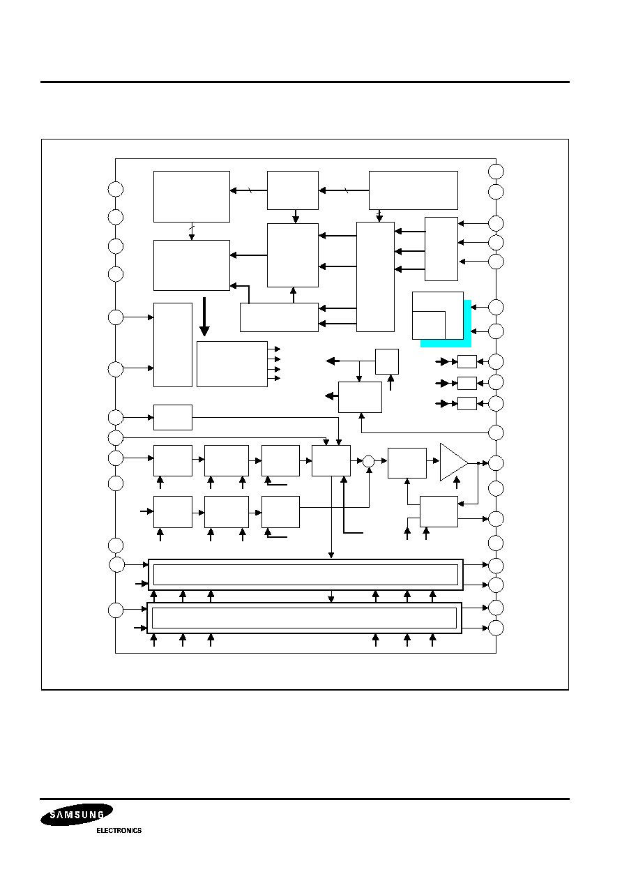
The S1D2502A01 is a very high frequency video amplifier
& wide range OSD processor 1 chip system with I
2
C Bus
control used in monitors. It contains 3 matched R/G/B video
amplifiers with OSD processor and provides flexible
interfacing to I
2
C Bus controlled adjustment systems.
FUNCTIONS
∑
R/G/B video amplifier
∑
OSD processor
∑
I
2
C bus control
∑
Cut-off brightness control
∑
R/G/B sub contrast/cut-off control
∑
Half tone
FEATURES
VIDEO AMP PART
∑
3-channel R/G/B video amplifier, 175MHz @f-3dB
∑
I
2
C bus control items
--
Contrast control: -38dB
--
Sub contrast control for each channel: -12dB
--
Brightness control
--
OSD contrast control: -38dB
--
Cut-off brightness control (AC coupling)
--
Cut-off control for each channel (AC coupling)
--
Switch registers for SBLK and video half tone and
CLP/BLK polarity selection and INT/EXT CLP selection
and generated CLP width control
∑
Built in ABL (automatic beam limitation)
∑
Built in video input clamp, BRT clamp
∑
Built in video half tone (3mode) function on OSD
pictures
∑
Capable of 8.0Vp-p output swing
∑
Improvement of rise & fall time (2.2ns)
∑
Cut-off brightness control
∑
Built in blank gate with spot killer
∑
Clamp pulse generator
∑
OSD intensity
∑
BLK, CLP polarity selection
∑
Clamp gate with anti OSD sagging
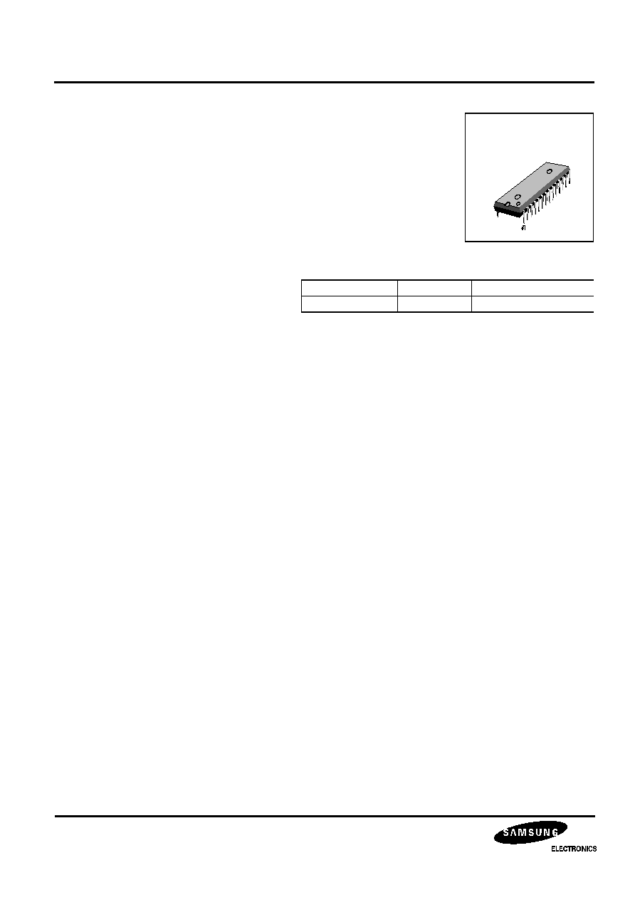
32-DIP-600A
ORDERING INFORMATION
Device
Package
Operating Temperature
S1D2502A01-D0B0
32-DIP-600A
-20
∞
C -- +75
∞
C
OSD PART
∑
Built in 1K-byte SRAM
∑
448 ROM fonts (each font consists of 12
◊
18
dots.)
∑
Full screen memory architecture
∑
Wide range PLL available (15kHz
--
96kHz,
Reference 800 X 600)
∑
Programmable vertical height of character
∑
Programmable vertical and horizontal
positioning
∑
Character color selection up to 16 different
colors
∑
Programmable background color (up to 16
colors)
∑
Character blinking, bordering and shadowing
∑
Color blinking
∑
Character scrolling
∑
Fade-in and fade-out
∑
Box drawing
∑
Character sizing up to four times
∑
76.8MHz pixel frequency from on-chip PLL
(Reference 800 X 600)
VIDEO AMP MERGED OSD PROCESSOR FOR MONITORS
S1D2502A01
3
Preliminary
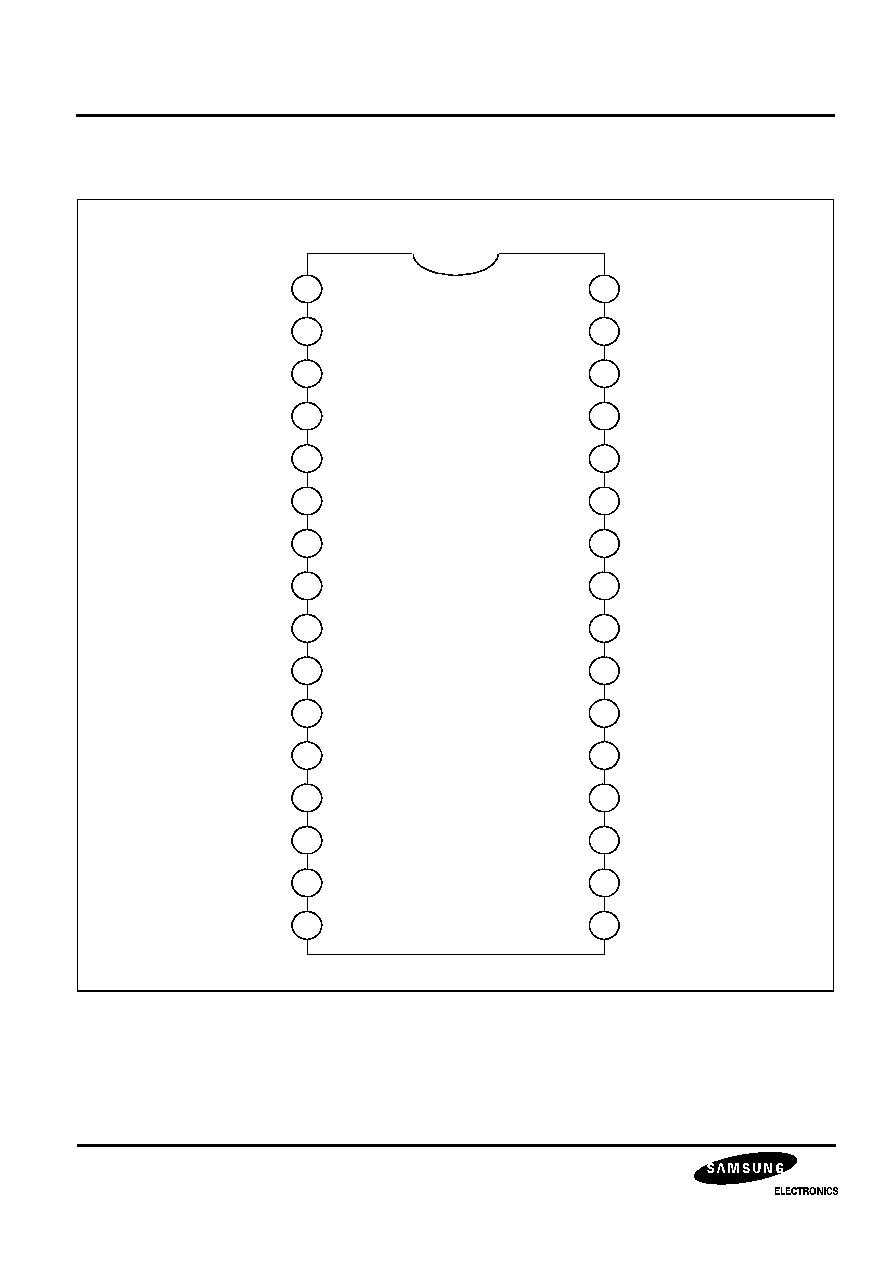
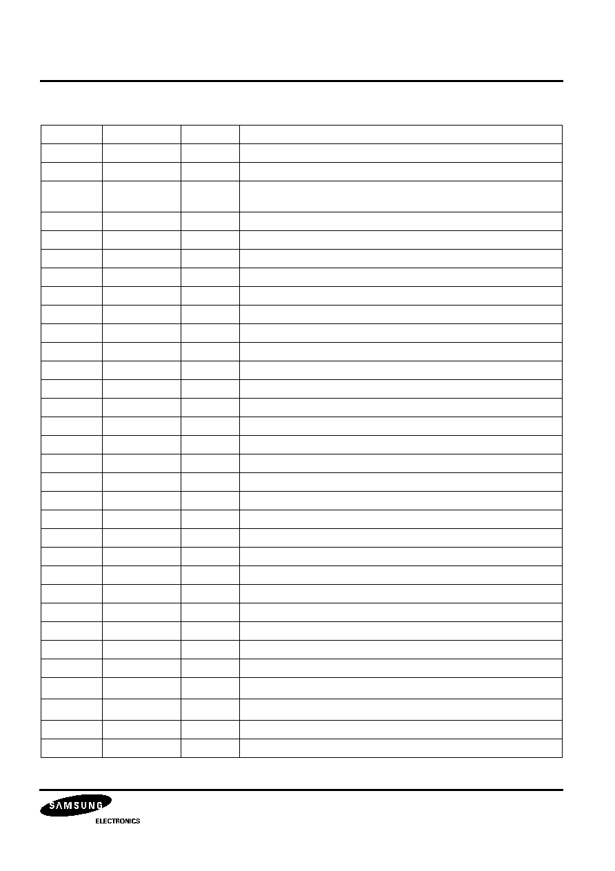
Table 1. Pin Configuration
Pin No.
Symbol
I/O
Configuration
1
VFLB
I
Vertical flyback signal
2
VSSA
-
Ground (PLL part)
3
VCO_IN_P
I
This voltage is generated at the external loop filter and goes into the
input stage of the VCO.
4
VREF1
O
Charge pump output
5
VREF
O
PLL regulator filter
6
VDDA
-
+5V supply voltage for PLL part
7
CONT_CAP
-
Contrast control for AMP part
8
ABL
-
Auto beam limit.
9
GND3
-
Ground for video AMP part(for AMP control)
10
CLP_IN
-
Video clamp pulse input
11
VCC3
-
+12V supply voltage for video AMP part(for AMP control)
12
RIN
I
Video signal input (red)
13
VCC1
-
+12V supply voltage for video AMP(for main video signal process)
14
GIN
I
Video signal input (green)
15
GND1
-
Ground for video AMP part(for main video signal process)
16
BIN
I
Video signal input (blue)
17
BCLP
-
B output clamp cap
18
BOUT
O
Video signal output (blue)
19
GND2
-
Ground for video AMP part(for video output drive)
20
GCLP
-
G output clamp cap
21
GOUT
O
Video signal output (green)
22
VCC2
-
+12V supply voltage for video AMP part(for video output drive)
23
RCLP
-
R output clamp cap
24
ROUT
O
Video signal output (red)
25
BCT
-
B cut-off output
26
GCT
-
G cut-off output
27
RCT
-
R cut-off output
28
VSS
-
Ground for digital part
29
SCL
I
Serial clock (I
2
C)
30
SDA
I/O
Serial data (I
2
C)
31
VDD
-
+5V supply voltage for digital part
32
HFLB
I
Horizontal flyback signal