
S1D2514X01 VIDEO AMP MERGED OSD PROCESSOR FOR MONITORS
0
Preliminary
VIDEO AMP MERGED OSD PROCESSOR
The S1D2514X01 is a very high frequency video amplifier
& wide range OSD processor 1 chip system with I
2
C Bus
control used in monitors. It contains 3 matched R/G/B video
amplifiers with OSD processor and provides flexible
interfacing to I
2
C Bus controlled adjustment systems.
FUNCTIONS
∑
R/G/B video amplifier
∑
OSD processor
∑
I
2
C bus control
∑
Cut-off brightness control
∑
R/G/B sub contrast/cut-off control
∑
Half tone
FEATURES
VIDEO AMP PART
∑
3-channel R/G/B video amplifier, 150MHz @f-3dB
∑
I
2
C bus control items
-- Contrast control: -38dB
- Sub contrast control for each channel: -12dB
- Brightness control
- OSD contrast control: -38dB
- Cut-off brightness control (AC coupling)
- Cut-off control for each channel (AC coupling)
- Switch registers for SBLK and video half tone and
CLP/BLK polarity selection and INT/EXT CLP selection
∑
Built in ABL (automatic beam limitation)
∑
Built in video input clamp, BRT clamp
∑
Built in video half tone (3mode) function on OSD
pictures
∑
Capable of 8.0Vp-p output swing
∑
Improvement of rise & fall time (2.2ns)
∑
Cut-off brightness control
∑
Built in blank gate with spot killer
∑
Clamp pulse generator
∑
OSD intensity
∑
BLK, CLP polarity selection
∑
Clamp gate with anti OSD sagging
32-DIP-600A
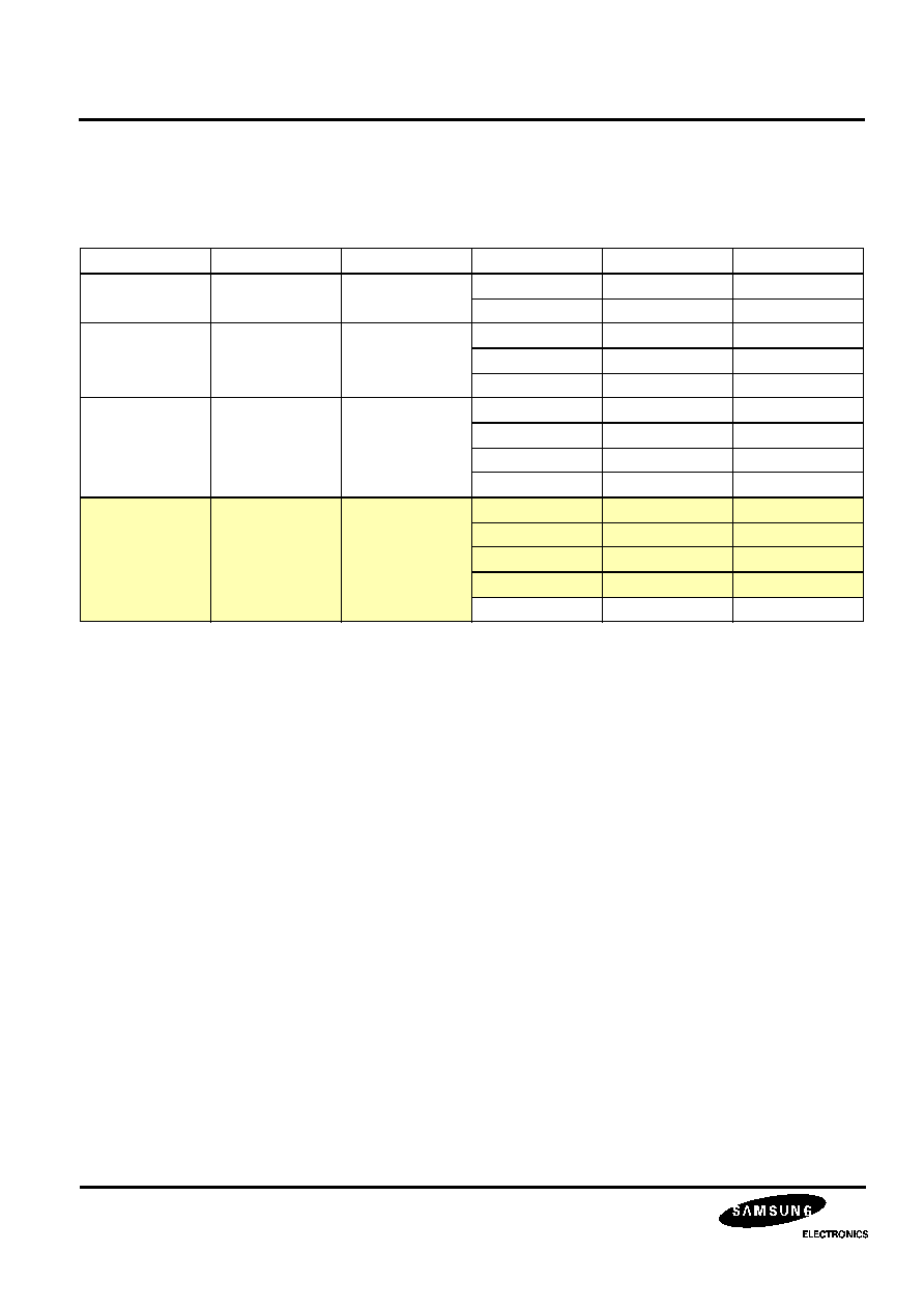
ORDERING INFORMATION
Device
Package
Operating Temperature
S1D2514X01-D0B0
32-DIP-600A
-20
∞
C
-
+75
∞
C
OSD PART
∑
Built in 1K-byte SRAM
∑
256 ROM fonts (each font consists of 12
◊
18
dots.)
∑
Full screen memory architecture
∑
Wide range PLL available (15kHz -- 90kHz,
Reference 800 X 600)
∑
Programmable vertical height of character
∑
Programmable vertical and horizontal
positioning
∑
Character color selection up to 16 different
colors (in a units of character)
∑
Programmable background color (up to 16
colors)
∑
Character blinking and shadowing
∑
Character scrolling
∑
72MHz pixel frequency from on-chip PLL
(Reference 800 ± 600)
∑
Full white pattern generation function

VIDEO AMP MERGED OSD PROCESSOR FOR MONITORS
S1D2514X01
1
Preliminary
BLOCK DIAGRAM
Figure 1. Functional Block Diagram
Latches
D/A
(448 x 18 x 12)
VDDA
(480 x 16)
OSD
Control
Display
Output Stage
Font Data
Timing Controller
Frame Ctrl
ROM Ctrl
Band
Gap.Ref
Multi (3 mode)
Half Tone
RGB OSD
FBL
INTE
HT DET.
BLK
Int
Clamp
Pulse
Gen.
CLP
BLK
HFLB
CLK
H_Pulse
V_Pulse
I
2
C bus
decoder
32
1
3
30
29
6
2
V/I
27
26
25
V/I
V/I
R cut off
G cut off
B cut off
R/G/B OSD
FBLK
Intensity
10
ABL
Video
Input
Clamp
Video
Half Tone
SW
Sub
Cont.
Control
Video
Contrast
OSD
Input
Cilp.
OSD
Half Tone
SW
OSD
Cont.
Control
I
2
C
I
2
C
I
2
C
FBLK
FBLK
I
2
C
CLP
HT DET.
12
7
R OSD
+
Sub
Cont.
Control
24
Birght
Control
BLK
CLP
I
2
C
22
23
I
2
C Cont. Cntl
G-CHANNEL
B-CHANNEL
CLP
HT DET.
FBLK
CLP
BLK
I
2
C
CLP
HT DET.
FBLK
CLP
BLK
I
2
C
16
14
G OSD
B OSD
13
15
8
5
4
9
11
28
31
20
21
17
18
VSSA
HFLB
VFLB
VCO_IN_P
SDA
SCL
RCT
GCT
BCT
CLP_IN
R OUT
VCC2
R CLP
G CLP
G OUT
B CLP
B OUT
VSS
VCC3
GND3
VREF1
VREF
ABL
CONT_CAP
RIN
GND1
VCC1
GIN
BIN
ROM
Address
RAM Data
9
16
16
Ctrl Data
12
Display Ctrl
H/V/CLK Ctrl
H/V/CLK Ctrl
Frame Ctrl
ROM Ctrl
Amp
Out
Ctrl Font
19
GND2

S1D2514X01 VIDEO AMP MERGED OSD PROCESSOR FOR MONITORS
2
Preliminary
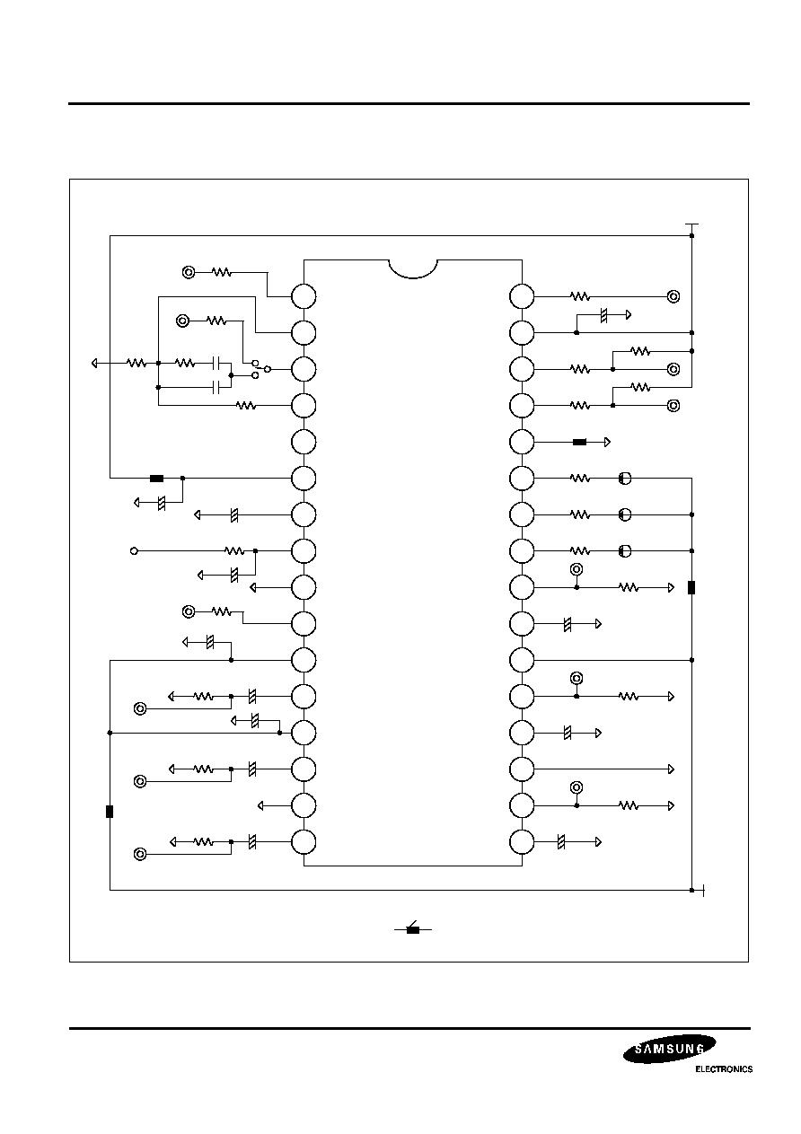
PIN CONFIGURATION
Figure 2. Pin Configuration
K
B
2
5
1
4
32
31
30
29
28
27
26
25
24
23
22
21
20
19
18
17
1
2
3
4
5
6
7
8
9
10
11
12
13
14
15
16
HFLB
VDD
SDA
SCL
VSS
RCT
GCT
BCT
ROUT
RCLP
VCC2
GOUT
GCLP
GND2
BOUT
BCLP
VFLB
VSSA
VCO_IN_P
VREF1
VREF
VDDA
CONT_CAP
ABL_IN
GND3
CLP_IN
VCC3
RIN
VCC1
GIN
GND1
BIN
S1D2514X01

VIDEO AMP MERGED OSD PROCESSOR FOR MONITORS
S1D2514X01
3
Preliminary
Table 1. Pin Configuration
Pin No.
Symbol
I/O
Configuration
1
VFLB
I
Vertical flyback signal
2
VSSA
-
Ground (PLL part)
3
VCO_IN_P
I
This voltage is generated at the external loop filter and goes into the
input stage of the VCO.
4
VREF1
O
Charge pump output
5
VREF
O
PLL regulator filter
6
VDDA
-
+5V supply voltage for PLL part
7
CONT_CAP
-
Contrast control for AMP part
8
ABL
-
Auto beam limit.
9
GND3
-
Ground for video AMP part(for AMP control)
10
CLP_IN
-
Video clamp pulse input
11
VCC3
-
+12V supply voltage for video AMP part(for AMP control)
12
RIN
I
Video signal input (red)
13
VCC1
-
+12V supply voltage for video AMP(for main video signal process)
14
GIN
I
Video signal input (green)
15
GND1
-
Ground for video AMP part(for main video signal process)
16
BIN
I
Video signal input (blue)
17
BCLP
-
B output clamp cap
18
BOUT
O
Video signal output (blue)
19
GND2
-
Ground for video AMP part(for video output drive)
20
GCLP
-
G output clamp cap
21
GOUT
O
Video signal output (green)
22
VCC2
-
+12V supply voltage for video AMP part(for video output drive)
23
RCLP
-
R output clamp cap
24
ROUT
O
Video signal output (red)
25
BCT
-
B cut-off output
26
GCT
-
G cut-off output
27
RCT
-
R cut-off output
28
VSS
-
Ground for digital part
29
SCL
I
Serial clock (I
2
C)
30
SDA
I/O
Serial data (I
2
C)
31
VDD
-
+5V supply voltage for digital part
32
HFLB
I
Horizontal flyback signal
S1D2514X01 VIDEO AMP MERGED OSD PROCESSOR FOR MONITORS
4
Preliminary
PIN DESCRIPTION
Table 2. Pin Description
Pin No
Pin Name
Schematic
Description
1
32
VFLB
HFLB
FLB signal is in TTL level
Multi polarity input
3
4
5
VCO_IN_P
VPEF1
VREF
PLL loop filter output
BandGap ref. output
7
Contrast cap
(CONT_CAP)
Contrast cap range
(0.1uF -- 5uF)
8
ABL_IN
ABL input DC range
(1 -- 4.5V)
VFLB
HFLB
4.0K
100
µ
A
Vref
I
2
C Data
2K
250
µ
A
Vref
Vref
100K
VCC

VIDEO AMP MERGED OSD PROCESSOR FOR MONITORS
S1D2514X01
5
Preliminary
10
CLP_IN
Multi polarity input
Clamp gate pulse TTL level
input
12
14
16
Red video input
(RIN)
Green video input
(GIN)
Blue video input
(BIN)
Max input video signal is 0.7
Vpp
17
20
23
Blue (B clamp cap)
Green (G clamp cap)
Red (R clamp)
Brightness controlling actives by
charging and discharging of the
external cap. (0.1
µ
F)
(During clamp gate)
Table 2. Pin Description (Continued)
Pin No
Pin Name
Schematic
Description
10K
50K
VCC
12K
0.2K
VCC
Video_In
VCC
CLP
0.2K
0.2K
Iclamp
S1D2514X01 VIDEO AMP MERGED OSD PROCESSOR FOR MONITORS
Preliminary
18
21
24
Blue video output
(BOUT)
Green video output
(GOUT)
Red video output
(ROUT)
Video signal output
27
26
25
Red cut-off control
(RCT)
Green cut-off control
(GCT)
Blue cut-off control
(BCT)
Cut-off control output
29
SCL
Serial clock input port of I
2
C bus
30
SDA
Serial data input port of I
2
C bus
Table 2. Pin Description (Continued)
Pin No
Pin Name
Schematic
Description
Isink
0.04K
VCC
Video_Out
0.5K
0.05K
CTX
0.2K
0-600uA 0-200uA 50uA 100uA
SCL
ACK
SDA

VIDEO AMP MERGED OSD PROCESSOR FOR MONITORS
S1D2514X01
7
Preliminary
ABSOLUTE MAXIMUM RATINGS
(see 1)
(Ta = 25
∞
C)
THERMAL & ESD PARAMETER
Table 3. Absolute Maximum Ratings
No
Item
Symbol
Value
Unit
Min
Typ
Max
1
Maximum supply voltage
V
CC
-
-
13.2
V
V
DD
-
-
6.5
2
Operating temperature
(see 2)
Topr
-20
-
75
∞
C
3
Storage temperature
Tstg
-65
150
∞
C
4
Operating supply voltage
V
CCop
11.4
12.0
12.6
V
(see 3)
V
DDop
4.75
5.00
5.25
5
Power dissipation
P
D
-
-
W
Table 4. Thermal & ESD Parameter
No
Item
Symbol
Value
Unit
Min
Typ
Max
1
Thermal resistance
(junction-ambient)
ja
-
48
-
∞
C/W
2
Junction temperature
Tj
-
150
-
∞
C
3
Human body model
(C = 100p, R = 1.5k)
HBM
2
-
-
KV
4
Machine model
(C = 200p, R = 0)
MM
300
-
-
V
5
Charge device model
CDM
800
-
-
V
S1D2514X01 VIDEO AMP MERGED OSD PROCESSOR FOR MONITORS
8
Preliminary
ELECTRICAL CHARACTERISTICS
DC ELECTRICAL CHARACTERISTICS
(Tamb = 25
∞
C, V
CC
= 12V, V
DD
= V
DDA
= 5V, ABL input voltage = 5V, HFLB input signal = S3, load resistors =
470
, except OSD part current 35
mA,
unless otherwise stated)
Table 5. DC Electrical Characteristics
Parameter
Symbol
Conditions
Value
Unit
Min
Typ
Max
Supply current
I
CC
(see 4)
100
125
130
mA
Minimum supply current
I
CC
min
V
CC
= 11.4V
95
110
120
mA
Maximum supply current
I
CC
max
V
CC
= 12.6V
105
130
140
mA
ABS supply current
I
CC
abs
V
CC
= 13.2V
-
-
175
mA
Video input bias voltage
V bias
1.8
2.1
2.4
V
Video black level voltage (POR)
V blackpor
1.20
1.50
1.80
V
Black level voltage channel difference (POR)
V blackpor
(see 5)
10
-
-
%
Video black level voltage (FFH)
V blackff
04 = FFH
(see 13)
2.2
2.7
3.2
V
Black level voltage channel difference (FFH)
V blackff
10
-
-
%
Video black level voltage (00H)
V black00
04 = 00H
-
0.2
0.5
V
Black level voltage channel difference (00H)
V black00
10
-
-
%
Spot killer voltage
Vspot
V
CC
= Var.
9.20
10.4
11.2
V
Cut-off current (FFH)
ICTff
Pin25, 26, 27 = 12V
09 -- 0B: FFH
0C: 00H
500
625
750
µ
A
Cut-off current (00H)
ICT00
Pin25, 26, 27 = 12V
09 -- 0C: 00H
-
2.0
5.0
µ
A
Cut-off brightness current (FFH)
ICTBRTff
Pin25, 26, 27 = 12V
09 -- 0B: 00H
0C: FFH
100
180
260
µ
A
Cut-off brightness current (80H)
ICTBRT80
Pin25, 26, 27 = 12V
09 -- 0B: 00H
0C: 80H
50
90
130
µ
A
Cut-off offset current 1
ICS1
Pin25, 26, 27 = 12V
09 -- 0C: 00H
0E: 11H
25
50
75
µ
A
VIDEO AMP MERGED OSD PROCESSOR FOR MONITORS
S1D2514X01
9
Preliminary
Total external cut-off current range
Cut-off offset current 2
ICS2
Pin25, 26, 27 = 12V
09 -- 0C: 00H
0E: 12H
50
100
130
µ
A
Soft BLK output voltage
Vsblk
0D: 80H
0E: 14H
-
0.2
0.5
V
Clamp cap voltage (POR)
Vcap
6.0
7.0
8.0
V
Table 5. DC Electrical Characteristics (Continued)
Parameter
Symbol
Conditions
Value
Unit
Min
Typ
Max
Red
cut-off
Creen
cut-off
Blue
cut-off
Cut-Off Brightness
CS2
CS1
Cut-Off Offset
Switch
600uA
200uA
100uA
50uA
150uA
S1D2514X01 VIDEO AMP MERGED OSD PROCESSOR FOR MONITORS
10
Preliminary
AC ELECTRICAL CHARACTERISTICS
(Tamb = 25
∞
C, V
CC
= 12V, V
DD
= V
DDA
= 5V, ABL input voltage = 5V, HFLB input signal = S3, load resistors =
470
, Vin = 0.7Vpp manually adjust video output pins 18, 21 and 24 to 4V DC for the AC test
(see 11)
unless
otherwise stated
(see 12)
)
Table 6. AC Electrical Characteristics
Parameter
Symbol
Conditions
Value
Unit
Min
Typ
Max
Contrast max. output voltage
Vcff
03, 05, 06, 07 = FFH
04, 08 -- 0C = 80H
RGB input = S1
5.0
5.7
6.4
Vpp
Contrast max. output channel difference
Vcff
10
-
-
%
Contrast center output voltage
Vc80
03, 04, 08 -- 0C = 80H
05, 06, 07 = FFH
RGB input = S1
2.5
2.85
3.2
Vpp
Contrast center output channel difference
Vc80
10
-
-
%
Contrast max. - Center attenuation
C
C = 20log (Vc80/Vcff)
-8
-6
-4
dB
Sub contrast center output voltage
Vd80
03 = FFH
04 -- 0C = 80H
RGB input = S1
2.3
2.6
2.9
Vpp
Sub contrast center output channel
difference
Vd80
10
-
-
%
Sub contrast min. output voltage
Vd00
03 = FFH, 05-- 07: 00H
04, 08 -- 0C = 80H
RGB input = S1
1.3
1.6
1.9
Vpp
Sub contrast min. output channel difference
Vd00
10
-
-
%
Sub contrast max. - min. attenuation
D
D = 20log (Vd00/Vcff)
-14
-12
-10
dB
ABL control range
ABL
(see 15)
-12
-10
-8
dB
R/G/B video rising time
(see 7)
tr (video)
03, 05 -- 07: FFH
04, 08 -- 0C: 80H
RGB input = S2
-
2.2
2.8
ns
R/G/B video falling time
(see 7)
tf (video)
-
2.2
2.8
ns
R/G/B blank output rising time
(see 7)
tr (blank)
POR
HFLB: S4
-
6.0
12.0
ns
R/G/B blank output falling time
(see 7)
tf (blank)
-
8.0
15.0
ns
R/G/B video band width
(see 7, 8)
f (-3dB)
(see 16)
150
-
-
MHz
Video AMP 50MHz cross talk
CT_50M
(see7, 9)
(see 17)
-
-25
-20
dB
Video AMP 130MHz cross talk
CT_130M
(see7, 9)
(see 18)
-
-15
-10
dB
Absolute gain match
Avmatch
(see 6)
-1
-
1
dB
Gain change between amplifier
Avtrack
(see 7)
-1
-
1
dB

VIDEO AMP MERGED OSD PROCESSOR FOR MONITORS
S1D2514X01
11
Preliminary
OSD ELECTRICAL CHARCTERISTICS
(Tamb = 25
∞
C, V
CC
= 12V, V
DD
= V
DDA
= 5V, HFLB input voltage = S3, load rosistors = 470
, V-AMP test
registor's FBLK, OSD input conditions unless otherwise stated)
Table 7. OSD Electrical Chaacteristics
Parameter
Symbol
Conditions
Value
Unit
Min
Typ
Max
OSD contrast max. output voltage
Vocff
08 = FFH
OSD RGB output conditions
5.4
6.4
7.4
Vpp
OSD contrast max. output channel
difference
Vocff
10
-
-
%
OSD contrast center output voltage
Voc80
08 = 80H
OSD RGB output conditions
2.7
3.2
3.7
Vpp
OSD contrast center output channel
difference
Voc80
10
-
-
%
R/G/B OSD rising time
tr (OSD)
08: FFH
-
4.0
5.0
ns
R/G/B OSD falling time
tf (OSD)
-
4.0
5.0
ns
HT video level
HTvideo
ABL = 6V
RGB input = S1
03, 05 -- 08: FFH
0D: 01H
OSD black conditions input
HTvideo = 20log(V
htvideo
/V
cff
)
-6.0
-4.5
-3.0
dB
HT video output channel difference
HTvideo
15
-
-
%
HT OSD level
HTosd
ABL = 6V
05 -- 08: FFH
0D: 0FH
OSD white condition input
HTosd = 20log (V
htosd
/
V
ocff
)
-7.0
-5.5
-4.0
dB
HT OSD output channel difference
HTosd
15
-
-
%

VIDEO AMP MERGED OSD PROCESSOR FOR MONITORS
12
Preliminary
OPERATION TIMINGS
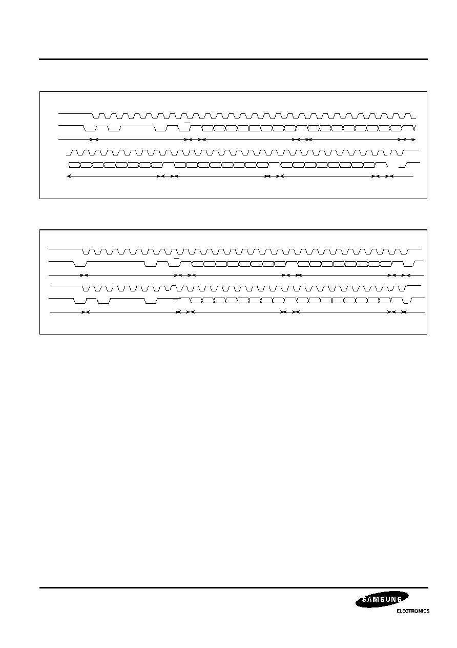
Table 8. Operation Timings
Parameter
Symbol
Min
Typ
Max
Unit
Input Signal HFLB, VFLB
Horizontal flyback signal frequency
f
HFLB
-
-
120
kHz
Vertical flyback signal frequency
f
VFLB
-
-
200
Hz
I
2
C Interface SDA, SCL (Refer to Figure 3)
SCL clock frequency
f
SCL
-
-
300
kHz
Hold time for start condition
t
hs
500
-
-
ns
Set up time for stop condition
t
sus
500
-
-
ns
Low duration of clock
t
low
400
-
-
ns
High duration of clock
t
high
400
-
-
ns
Hold time for data
t
hd
0
-
-
ns
Set up time for data
t
sud
500
-
-
ns
Time between 2 access
t
ss
500
-
-
ns
Fall time of SDA
t
fSDA
-
-
20
ns
Rise time of both SCL and SDA
t
rSDA
-
-
-
ns
Figure 3. I
2
C Bus Timing Diagram
SDA
SCL
ths
tsud
tss
thd
thigh
tlow
tsus

VIDEO AMP MERGED OSD PROCESSOR FOR MONITORS
S1D2514X01
13
Preliminary
OSD PART DC ELECTRICAL CHARACTERISTICS
(Ta = 25 C, V
DDA
DD
= 5V)
Parameter
Symbol
Typ
Max
Supply voltage
V
4.75
5.00
V
Supply current
I
DD
-
25
Input voltage
V
0.8V
DD
-
V
IL
-
V
SS
V
Output voltage
±
1mA)
OH
0.8V
-
-
V
OL
-
V
+ 0.4
V
I
IL
-
10
A
VCO input voltage
VCO
2.5

S1D2514X01 VIDEO AMP MERGED OSD PROCESSOR FOR MONITORS
14
Preliminary
NOTES:
1.
Absolute maximum rating indicates the limit beyond which damage to the device may occur.
2.
Operating ratings indicate conditions for which the device is functional but do not guarantee specific performance limits.
For guaranteed specifications and test conditions, see the electrical characteristics. The guaranteed specifications apply
only for the test conditions listed. Some performance characteristics may degrade when the device is not operated under
the listed test conditions.
3.
V
CC
supply pins 11, 13, and 22 must be externally wired together to prevent internal damage during V
CC
power on/off
cycles.
4.
The supply current specified is the quiescent current for VCC
1
/VCC
2
and VCC
3
with RL =
, The supply current
for VCC2 (pin 22) also depends on the output load.
5.
Output voltage is dependent on load resistor. Test circuit uses RL = 470
6.
Measure gain difference between any two amplifiers Vin = 700mVpp.
7.
When measuring video amplifier bandwidth or pulse rise and fall times, a double sided full ground plane printed circuit
board without socket is recommended. Video amplifier 50MHz cross talk test also requires this printed circuit board. The
reason for a double sided full ground plane PCB is that large measurement variations occur in single sided PCBs.
8.
Adjust input frequency from 10MHz (AV max reference level) to the -3dB frequency (f -3dB).
9.
Measure output levels of the other two undriven amplifiers relative to the driven amplifier to determine channel separation.
Terminate the undriven amplifier inputs to simulate generator loading. Repeat test at fin = 50MHz for cross talk 50MHz.
10. A minimum pulse width of 200 ns is guaranteed for a horizontal line of 15kHz. This limit is guaranteed by design. if a lower
line rate is used a longer clamp pulse may be required.
11. During the AC test the 4V DC level is the center voltage of the AC output signal. For example. If the output is 4Vpp the
signal will swing between 2V DC and 6V DC.
12. These parameters are not tested on each product which is controlled by an internal qualification procedure.
13. The conditions block's 03, 04, 05... etc. signify sub address' 0F03, 0F04, 0F05... etc.
14. Sub address 0F03, 0F05 -- 0F07: FFH
0F04, 0F08 -- 0F0C: 80H
RGB input = S1,
When the ABL input voltage is 0V, the R/G/B's output voltage is VR/VG/VB and uses the formula ABLR = 20log (VR/V
cffR
)
15. OSD TST mode = High, CLP operation off,
RGB input = S5 (frequency sweep),
RGB input clamp cap = 2.1V DC,
RGB clamp cap (pin 23/20/17) = Vcap voltage (7.0V),
S5's frequency 1MHz
130MHz sweep, -3dB point = 20log (V
130MHz
/
V
1MHz
)
03, 05 -- 07: FFH
04, 08 -- 0C: 80H
0F: 80H
16. OSD TST mode = High, CLP operation off,
RGB input clamp cap = 2.1V DC,
RGB clamp cap (pin 23/20/17) = Vcap voltage (7.0V),
03, 05 -- 07: FFH
04, 08 -- 0C: 80H
0F: 80H
R input = S5 (50MHz)
CT_50M = 20log (V
outG
/V
outR
) or 20log (V
outB
/
V
outR
)
17. OSD TST mode = High, CLP operation off,
RGB input clamp cap = 2.1V DC,
RGB clamp cap (pin 23/20/17) = Vcap voltage (7.0V),
03, 05 -- 07: FFH
04, 08 -- 0C: 80H
0F: 80H
R input = S5 (130MHz)
CT_150M = 20log (V
outG
/V
outR
) or 20log (V
outB
/V
outR
)
VIDEO AMP MERGED OSD PROCESSOR FOR MONITORS
S1D2514X01
Preliminary
TEST SIGNAL FORMAT
∑
S1, S2 signal's low level must be synchronized with the S3 signal's sync. term.
∑
The input signal level uses the IC pin as reference.
Table 10. Test Signal Format
Signal
Name
Input Signal Formal
Signal Description
S1
Video gain measurement
Video = 1MHz/0.7Vpp
Sync = 50kHz
S2
Video Tr/Tf measurement
f = 200kHz
V = 0.7Vpp
Duty = 50%
S3
HFLB (posi & nega.) input
f = 50kHz
t = 2uS
V = 0V/5V
S4
OSD level measurement
Blank Tr/Tf measurement
f = 50kHz
V = 0V/5V
S5
Crosstalk test
Bandwidth measurement
1MHz/10MHz/50MHz/
130MHz
Vref = input clamp voltage
Vi = 0.7Vpp
Sync
[V]
4uS
[t]
Video
[V]
[t]
Vpp
0.7
f = 200kHz
Duty = 50%
[t]
t = 2uS
[V]
f = 50kHz
0V
5V
[V]
[t]
f = 200kHz
Duty = 50%
[V]
[t]
Vref
[V]
Vi
S1D2514X01 VIDEO AMP MERGED OSD PROCESSOR FOR MONITORS
16
Preliminary
TEST CIRCUIT
Figure 4. Test Circuit
1
2
3
4
5
6
7
8
9
10
11
12
13
14
15
16
32
31
30
29
28
27
26
25
24
23
22
21
20
19
18
17
VFLB
VSSA
VCO_IN_P
VREF1
VREF
VDDA
CONT_CAP
ABL_IN
GND3
CLP_IN
VCC3
RIN
VCC1
GIN
GND1
BIN
HFLB
VDD
SDA
SCL
VSS
RCT
GCT
BCT
ROUT
RCLP
VCC2
GOUT
GCLP
GND2
BOUT
BCLP
KB2514
Magnetic core
33
BNC1
33
BNC2
10uF
5.6K
33pF
1M
27K
1
2
SW1
100u
1u
100
1u
ABL
33
BNC6
100u
75
0.1u
100u
BNC7
BNC8
75
0.1u
0.1u
75
BNC9
0.1u
470
0.1u
470
0.1u
470
2K
2K
2K
33
4.7K
BNC5
BNC5
4.7K
33
100u
BNC3
33
V
DD
= 5.0V
V
SS
= 12.0V
S1D2514X01
VIDEO AMP MERGED OSD PROCESSOR FOR MONITORS
S1D2514X01
17
Preliminary
FUNCTIONAL DESCRIPTIONS
DATA TRANSMISSION
The interface between S1D2514X01 and MCU follows the I
2
C protocol. After the starting pulse, the transmission
takes place in the following order: Slave address with R/W bit, 2-byte register address, 2-byte data, and stop
condition. an acknowledge signal is received for each byte, excluding only the start/stop condition. The 2-byte
register address is composed of an 8-bit row address, and an 8-bit column address. The order of transmission for
a 2-byte register address is 'Row address
Column address'. The 2 bytes of data is because S1D2514X01 has a
16-bit base register configuration. S1D2514X01's slave address is BAh. It is BBh in read mode, and BAh in write
mode.
∑
Address Bit Pattern for Display Registers Data
(a) row address bit pattern
R3 - R0: Valid data for row address
(b) Column address bit pattern
C4 - C0: Valid data for column address
X:Don't care bit
∑
Data Transmission Format
A15
A14
A13
A12
A11
A10
A9
A8
X
X
X
X
R3
R2
R1
R0
A7
A6
A5
A4
A3
A2
A1
A0
X
X
X
C4
C3
C2
C1
C0
Figure 5. Data Transmission Format at Writing Operation
Figure 6. Data Transmission Format at Reading Operation
Start
Slave address
ACK
Row address
ACK
Column address
ACK
Data byte N
ACK
Data byte N+1
ACK
Stop
Start
Slave address
ACK
Row address
ACK
Column address
ACK
Stop
Start
Slave address
ACK
Data byte N
ACK
Data byte N+1
ACK
Stop
S1D2514X01 VIDEO AMP MERGED OSD PROCESSOR FOR MONITORS
18
Preliminary
∑
SDA / SCL Signal At Communication
Figure 7. SDA line and SCL line (Write Operation)
Figure 8. SDA line and SCL line (Read Operation)
SDA
A5
A4
A3
A2
A1
A0
A6
A7
A9
A8
A10
A11
A12
A13
A14
A15
R/W
SCL
START
IIC SLAVE ADDRESS
ACK
MSB ADDRESS
ACK
LSB ADDRESS
ACK
SCL
D1
D0
D2
D3
D4
D5
D6
D7
SDA
D1 D0
D2
D3
D4
D5
D6
D7
ACK
DATA BYTE N(MSB DATA)
ACK
STOP
ACK
DATA BYTE N(LSB DATA)
D1
D0
D2
D3
D4
D5
D6
D7
DATA BYTE N(MSB DATA)
...
...
SDA
A5
A4
A3
A2
A1
A0
A6
A7
A9
A8
A10
A11
A12
A13
A14
A15
R/W
SCL
START
IIC SLAVE ADDRESS
ACK
MSB ADDRESS
ACK
LSB ADDRESS
ACK
SCL
D9
D8
D10
D11
D12
D13
D14
D15
SDA
D1 D0
D2
D3
D4
D5
D6
D7
ACK
DATA BYTE N(LSB)
ACK STOP
ACK
DATA BYTE N(MSB)
STOP
R/W
START
IIC SLAVE ADDRESS

VIDEO AMP MERGED OSD PROCESSOR FOR MONITORS
S1D2514X01
19
Preliminary
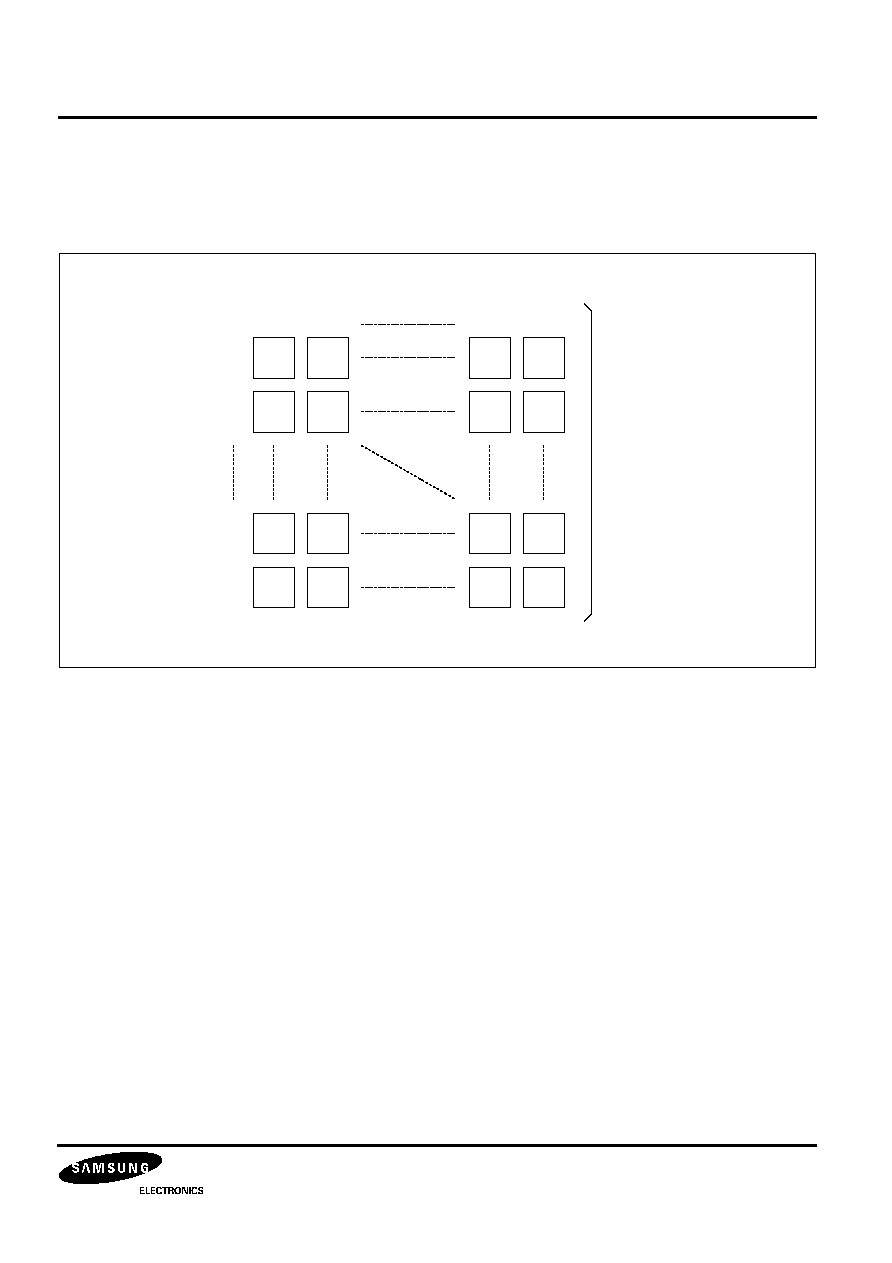
MEMORY MAP
The display RAM's address of the row and column number are assigned in order. The display RAM is composed of
3 register groups (character & attribute register, frame control register and V-AMP control register).
The display area in the monitor screen is 30 column
◊
15 row, so the related character & attribute registers are also
30 column
◊
15 row. Each register has a character address and characteristics corresponding to the display
location on the screen, and one register is composed of 16 bits. The lower 8 bits select the font from the 256 ROM
fonts, and the upper 8 bits give font characteristics to the selected font.
The frame control registers are in the 16th row. It controls OSD's display location, character height and scroll in
units of frame.
The V-AMP control registers are also located in the 17th row.
Figure 9. Memory Map of Display Registers
00 01 02 03
00 01
00
01
02
13
14
12
Character & Attribute Registers [Display RAM]
(30 x15 Character Display)
Frame Control Registers
Video-AMP Control Registers
15
Row
Row
Row
Row
Row
Row
00 01 02 03 04 05
Row 16
27 28 29

S1D2514X01 VIDEO AMP MERGED OSD PROCESSOR FOR MONITORS
20
Preliminary
REGISTER DESCRIPTION
Character & Attribute Register: Row00 ~ 14, Column00 ~ 29
Frame Control Register 0: Row15, Column00
Frame Control Register 1: Row15, Column01
Frame Control Register 2: Row15, Column02
Blink SHA
RB
RG
RR
CB
CG
CR
C7
C6
C5
C4
C3
C2
C1
C0
F
E
D
C
B
A
9
8
7
6
5
4
3
2
1
0
Character Code (256 fonts)
Character Attribute
Extended Code
CTL1
CTL0
-
-
-
-
-
-
-
FullW EX-EN BGEN ScrEN
ScrT
BliEN
BliT
Erase
EN
F
E
D
C
B
A
9
8
7
6
5
4
3
2
1
0
CP1
CP0
Fpll
HF2
HF1
HF0
dot1
dot0 HPOL VPOL CH5
CH4
CH3
CH2
CH1
CH0
F
E
D
C
B
A
9
8
7
6
5
4
3
2
1
0
Character Height Control
Polarity
PLL Control
Frame Control Register 3: Row15, Column03
HP7
HP6
HP5
HP4
HP3
HP2
HP1
HP0
VP7
VP6
VP5
VP4
VP3
VP2
VP1
VP0
F
E
D
C
B
A
9
8
7
6
5
4
3
2
1
0
Vertical Start Posiotion
Horizontal Start Posiotion
Blink SHA RINT CINT
F
E
D
C
B
A
9
8
7
6
5
4
3
2
1
0
CTL11
Blink SHA RINT CINT Blink SHA RINT CINT Blink SHA RINT CINT
CTL10
CTL01
CTL00

VIDEO AMP MERGED OSD PROCESSOR FOR MONITORS
S1D2514X01
21
Preliminary
Figure 10. Register Description
'
-
' ; Don't care bit
Video AMP Control Register: Row 16, Column 00 - 05
BRT7
BRT6
BRT5 BRT4
BRT3
BRT2
BRT1 BRT0
VC7
VC6
VC5
VC4
VC3
VC2
VC1
VC0
F
E
D
C
B
A
9
8
7
6
5
4
3
2
1
0
Contrast Control
Brightness Control
Column 00
GSB7 GSB6 GSB5 GSB4 GSB3 GSB2 GSB1 GSB0 RSB7 RSB6 RSB5 RSB4 RSB3 RSB2 RSB1 RSB0
F
E
D
C
B
A
9
8
7
6
5
4
3
2
1
0
R SUB Contrast Control
G SUB Contrast Control
Column 01
OSD7 OSD6 OSD5 OSD4 OSD3 OSD2 OSD1 OSD0 BSB7
BSB6
BSB5
BSB4
BSB3
BSB2
BSB1
BSB0
F
E
D
C
B
A
9
8
7
6
5
4
3
2
1
0
B SUB Contrast Control
OSD Contrast Control
Column 02
GWB7 GWB6 GWB5 GWB4 GWB3 GWB2 GWB1 GWB0 RWB7 RWB6 RWB5 RWB4 RWB3 RWB2 RWB1 RWB0
F
E
D
C
B
A
9
8
7
6
5
4
3
2
1
0
R Cut-off Control
G Cut-off Control
Column 03
CUT7 CUT6 CUT5 CUT4 CUT3 CUT2 CUT1 CUT0 BWB7 BWB6 BWB5 BWB4 BWB3 BWB2 BWB1 BWB0
F
E
D
C
B
A
9
8
7
6
5
4
3
2
1
0
B Cut-off Control
Cut-off Brightness Control
Column 04
CLPS CLPP BLKP
CS2
CS1
HG3
HR3
HB3
SB
HG2
HR2
HB2
HG1
HR1
HB1
HT
F
E
D
C
B
A
9
8
7
6
5
4
3
2
1
0
Column 05

S1D2514X01 VIDEO AMP MERGED OSD PROCESSOR FOR MONITORS
22
Preliminary
Table 11. Register Description
Registers
Bits
Description
Character &
Attribute Registers
(Row 00 ~ 14,
Column 00 ~ 29)
C7 -- C0
(Bit 7 -- 0)
Character code address
This is the address of 256 ROM fonts.
CB, CG, CR
(Bit A -- 8)
Character color
The character color is chosen from 16 colors using these 3 bits and the
frame control register 3's CINT bit.
RB, RG, RR
(Bit D -- B)
Raster color is determined by these bits.
The raster color is chosen from out of 16 colors using these 3 bits and the
frame control register 3's RINT bit.
SHA / CTL0
(Bit E)
Character shadowing / CTL0(Extended Code)
If you set the frame control register 0's EX-EN bit to '0', this bit carries out
character shadowing feature.( If SHA bit is '1', the character shadowing is
shown)
If you set the frame control register 0's EX-EN bit to '1', this bit is used for
extended code.
Blink / CTL1
(BIt F)
Character blinking / CTL1(Extended Code)
If you set the frame control register 0's EX-EN bit to '0', this bit carries out
character blinking feature.( If Blink bit is '1', the character blinking feature is
shown)
If you set the frame control register 0's EX-EN bit to '1', this bit is used for
extended code.
If you set the Frame Control Register 0's 'EX-EN' bit as '1', the Character & Attribute Register's 'SHA' and 'Blink'
bits are used to call the Extended Code.
In other words, the combination of SHA and Blink bits can call four kind Extended Code 'CTL00', 'CTL01',
'CTL10' and 'CTL11', the CINT, RINT, SHA and Blink features can be carried out in a unit of character fonts.

VIDEO AMP MERGED OSD PROCESSOR FOR MONITORS
S1D2514X01
23
Preliminary
Frame Control
Registers - 0
(Row15,
Column00)
EN
(Bit 0)
OSD enable
OSD is enabled when this bit is '1'. In other words, if this bit isn't '1'OSD is
not output inspite of writing control data. We recommend that you enable
the OSD after setting the control registers (such as the character & attribute
register) because of video and OSD output timing.
Erase
(Bit 1)
RAM erasing
If this bit is '1', the RAM data (character & attribute registers) is erased. The
time spent in carrying out this operation is called erasing time, which can be
calculated as follows.
Therefore, the maximum erasing time value is:
BliT
(Bit 2)
Blink time control
If this bit is '1', blink time is 0.5sec, and if not, 1sec.
BliEN
(Bit 3)
Blinking enable
Blinking effect is controlled by this bit.
If this bit is '1', blinking effect is enabled.
If this bit is '0', a full OSD screen blinking effect is disabled.
ScrT
(Bit 4)
Scroll time control
If this bit is '1', scroll time is 0.5sec, and if not, 1sec.
ScrEN
(Bit 5)
Scroll enable
Scrolling effect is controlled by this bit. If this bit is '1', scrolling effect is
enabled. You must remember that scrolling can be turned on/off only when
OSD is enabled/disabled.
BGEN
(Bit 6)
Back ground enable
If the BGEN bit is '1' and the raster color is black, the raster is transparent.
That is, the video back ground is shown. If not, the OSD raster covers the
video's back ground. Refer to other color effect.
EX-EN
(Bit 7)
Extended code enable
If the EX-EN bit is '1', the Character & Attribute register's Blink, SHA bits
carry out Extended Code features instead of Blink and SHA features.
FullW
(Bit 8)
Full white pattern enable
If the FullW bit is '1', the full white pattern is displayed in the screen.
Table 11. Register Description (Continued)
Registers
Bits
Description
Erasing time = RAM clock
◊
480 (RAM cell no.)
RAM clock = 12 dot clock
Dot clock = 1/(dot frequency)
Dot frequency = Horizontal frequency
◊
resolution (mode)
(Erasing Time)
MAX
= (12
◊
480) / (15k
◊
320) = 1.2ms

S1D2514X01 VIDEO AMP MERGED OSD PROCESSOR FOR MONITORS
Frame Control
Registers - 1
Column01)
CH5 -- CH0 Character height control
While the purpose of VZ[1:0] (vertical character height) is to control the
to output OSD of a uniform size even if the resolution changes. If you adjust
the value in the range of CH = 18 ~ CH = 63, each line's repeating number
line is repeated. For more information on repeating number selection, refer
to character height.
(Bit 6)
Polarity of vertical fly back signal
words, this bit is set to '1' if active high, and '0' if active low.
HPOL
Polarity of horizontal fly back signal
If this bit is '1', HFLB's polarity is positive, and if '0', it is negative. In other
dot1, dot0
(Bit 9, 8)
As shown above, the number of dots per horizontal line is decided by a
combination of these two bits.
(Bit C -- A)
Horizontal frequency
This is related to the selection of DOT[1:0], so you can't numerically
express the frequency range with only the HF[2:0] selection. For more
FPLL
(Bit D)
If this bit is '1', the OSD_PLL block's VCO operates at full range (4.8MHz -
96MHz). If it is '0', it operates within the region decided by the HF bit [C:A]
the high region, you may set the FPLL bit to '1'.
Table 11. Register Description
Registers
Bits
Dot1
Dot0
0
0
0
1
1
0
1
1
VIDEO AMP MERGED OSD PROCESSOR FOR MONITORS
S1D2514X01
25
Preliminary
The purpose of bits 'HPOL', and 'VPOL' is to provide flexibility when using the S1D2514X01 IC. No matter which
polarity you choose for the input signal, the IC will handle them identically, so you can select active high or active
low according to your convenience.
Frame Control
Registers - 1
(Row15,
Column01)
CP1, CP0
(Bit F, E)
Charge pump output current control
This is the PLL block's internal phase detector output status, converted into
current. Refer to PLL control.
The output is decided by the combination of these two bits.
Table 11. Register Description (Continued)
Registers
Bits
Description
CP1
CP0
Charge Pump Current
0
0
0.50 mA
0
1
0.75 mA
1
0
1.00 mA
1
1
1.25 mA

VIDEO AMP MERGED OSD PROCESSOR FOR MONITORS
26
Preliminary
Tabel 4. Register Description (Continued)
Registers
Bits
Description
Frame Control
Registers - 2
(Row 15,
Column 02)
VP7 -- VP0
(Bit 7 -- 0)
Vertical start position control ( = VP[7:0]
◊
4)
Signifies top margin height from the V-Sync reference edge.
HP7 -- HP0
(Bit F -- 8)
Horizontal start position control ( = HP[7:0]
◊
6)
Signifies delay of the horizontal display from the H-Sync reference edge to
the character's 1st pixel location.
Frame Control
Registers - 3
(Row 15,
Column 03)
CTL 00
(Bit 3 -- 0)
Extended code
In case the EX-EN bit is '1' and the Character & Attribute register's E and F
bits are '0', these bits have meanings.
If you set the CINT(character color intensity) bit '1', the character color
intensity feature is carried out.
If you set the RINT(raster color intensity) bit '1', the raster color intensity
feature is carried out.
If you set the SHA(character shadowing) bit '1', the character shadowing
feature is carried out.
If you set the Blink(character blinking) bit '1', the character blinking feature
is carried out.
CTL 01
(Bit 7 -- 4)
Extended code
In case the EX-EN bit is '1' and the Character & Attribute register's E bit is
'1' and F bit is '0', these bits have meanings.
If you set the CINT(character color intensity) bit '1', the character color
intensity feature is carried out.
If you set the RINT(raster color intensity) bit '1', the raster color intensity
feature is carried out.
If you set the SHA(character shadowing) bit '1', the character shadowing
feature is carried out.
If you set the Blink(character blinking) bit '1', the character blinking feature
is carried out.
CTL 10
(Bit B -- 8)
Extended code
In case the EX-EN bit is '1' and the Character & Attribute register's E bit is
'0' and F bit is '1', these bits have meanings.
If you set the CINT(character color intensity) bit '1', the character color
intensity feature is carried out.
If you set the RINT(raster color intensity) bit '1', the raster color intensity
feature is carried out.
If you set the SHA(character shadowing) bit '1', the character shadowing
feature is carried out.
If you set the Blink(character blinking) bit '1', the character blinking feature
is carried out.

VIDEO AMP MERGED OSD PROCESSOR FOR MONITORS
S1D2514X01
27
Preliminary
Frame Control
Registers - 3
(Row 15,
Column 03)
CTL 11
(Bit F -- C)
Extended code
In case the EX-EN bit is '1' and the Character & Attribute register's E and F
bits are '1', these bits have meanings.
If you set the CINT(character color intensity) bit '1', the character color
intensity feature is carried out.
If you set the RINT(raster color intensity) bit '1', the raster color intensity
feature is carried out.
If you set the SHA(character shadowing) bit '1', the character shadowing
feature is carried out.
If you set the Blink(character blinking) bit '1', the character blinking feature
is carried out.
Tabel 4. Register Description (Continued)
Registers
Bits
Description

S1D2514X01 VIDEO AMP MERGED OSD PROCESSOR FOR MONITORS
28
Preliminary
Tabel 4. Register Description (Continued)
Registers
Bits
Description
V-AMP Control
Registers - 0
(Row 16,
Column 00)
VC7 -- VC0
(Bit7 -- 0)
The contrast adjustment is made by contrdling simultaneously the gain
of three internal variable gain amplifiers.
The contrast adjustment allows to cover a typical range of 38dB.
BRT7 -- BRT0
(BitF -- 8)
The brightness adjustment controls to add the same black level
(pedestal) to the 3-channel R/G/B signals after contrast amplifier.
V-AMP Control
Registers - 1
(Row 16,
Column 01)
RSB7 -- RSB0
(Bit7 -- 0)
R channel SUB contrast control.
The SUB contrast adjustment is used to adjust the white balance, and
the gain of each channel is controlled.
The SUB contrast adjustment allows you to cover a typical tange of
12dB.
GSB7 -- GSB0
(BitF -- 8)
G channel SUB contrast control.
The SUB contrast adjustment is used to adjust the white balance, and
the gain of each channel is controlled.
The SUB contrast adjustment allows you to cover a typical tange of
12dB.
V-AMP Control
Registers - 2
(Row 16,
Column 02)
BSB7 -- BSB0
(Bit7 -- 0)
B channel SUB contrast control.
The SUB contrast adjustment is used to adjust the white balance, and
the gain of each channel is controlled.
The SUB contrast adjustment allows you to cover a typical tange of
12dB.
OSD7 -- OSD0
(BitF -- 8)
The OSD contrast adjustment is made by contrdling simultaneously the
gain of three internal variable gain amplifiers.
The OSD contrast adjustment allows to cover a typical range of 38dB.
V-AMP Control
Registers - 3
(Row 16,
Column 03)
RWB7 -- RWB0
(Bit7 -- 0)
R channel cut-off control.
The cut-off adjustment is used to adjust the raster white balance.
GWB7 -- GWB0
(BitF -- 8)
G channel cut-off control.
The cut-off adjustment is used to adjust the raster white balance.
V-AMP Control
Registers - 4
(Row 16,
Column 04)
BWB7 -- BWB0
(Bit7 -- 0)
B channel cut-off control.
The cut-off adjustment B used to adjust the raster white balance.
CUT7 -- CUT0
(BitF -- 8)
The cut-off brightness adjustment is made by simultaneously controlling
the external cut-off current.
VIDEO AMP MERGED OSD PROCESSOR FOR MONITORS
S1D2514X01
29
Preliminary
V-AMP Control
Registers - 5
(Row 16,
Column 05)
HT
(Bit 0)
Video & OSD half tone enable.
If you set this bit to '1', the half tone function is on.
Then you can see the video signal & OSD raster.
HG1 -- HB1
(Bit3 -- 1)
HG1 -- HB1 bits select OSD raster color 1 to be half tone.
To carry out half tone function, set the HT bit to '1'.
HG2 -- HB2
(Bit6 -- 4)
HG2 ~ HB2 bits select OSD raster color 2 to be half tone.
To carry out half tone function, set the HT bit to '1'.
SB
(Bit 7)
Soft blanking enable
If you set this bit '1', the R/G/B outputs go to GND.
Tabel 4. Register Description (Continued)
Registers
Bits
Description
HG1
HR1
HB1
OSD
Raster
Color 1
POR
G
R
B
0
0
0
0
0
0
Black
O
0
0
1
0
0
1
Blue
0
1
0
0
1
0
Red
0
1
1
0
1
1
Magenta
1
0
0
1
0
0
Green
1
0
1
1
0
1
Cyan
1
1
0
1
1
0
Yellow
1
1
1
1
1
1
White
HG2
HR2
HB2
OSD
Raster
Color 2
POR
G
R
B
0
0
0
0
0
0
Black
O
0
0
1
0
0
1
Blue
0
1
0
0
1
0
Red
0
1
1
0
1
1
Magenta
1
0
0
1
0
0
Green
1
0
1
1
0
1
Cyan
1
1
0
1
1
0
Yellow
1
1
1
1
1
1
White

S1D2514X01 VIDEO AMP MERGED OSD PROCESSOR FOR MONITORS
30
Preliminary
Registers - 5
(Row 16,
HG3 -- HB3
(BitA -- 8)
To carry out half tone function, set the HT bit to '1'.
CS2 -- CS1
Cut-off offset current control
BLKP
Polarity of horizontral fly back signal
If this bit is '0', HFLB's polarity is negative, and if '1', it is positive.
(Bit E)
Polarity of clamp pulse signal
This bit has meaning only if the CLPS bit is set to '1'.
CLPS
Clamp pulse generation enable
If this bit is '0', clamp signal is made using the HFLB signal, so there is
and if '1' you must supply external clamp signal.
Tabel 4. Register Description (Continued)
Bits
Description
HR3
HB3
Raster
Color 3
G
R
1
0
0
0
Black
1
1
0
1
Blue
1
0
1
0
1
1
0
1
Magenta
0
0
1
0
Green
0
0
1
0
Cyan
0
0
1
0
Yellow
1
1
1
1
CS2
CS1
POR
0
100
µ
0
1
µ
A
0
0 A
O
1
50 A

VIDEO AMP MERGED OSD PROCESSOR FOR MONITORS
S1D2514X01
31
Preliminary
VIDEO AMP PART ADDRESS MAP
Register sub address
Contrast Register (SUB ADRS: 00H) (Vin = 0.7Vpp, bright: 80H, subcont: FFH)
Brightness Register (3-ch) (SUB ADRS: 00H) (cont: 80H, subcont: 80H)
SUB Contrast Register (R/G/B-ch) (SUB ADRS: 01/02H)
(Vin = 0.7Vpp, bright: 40H, cont: FFH)
Table 12. Video AMP Part Address Map
SUB
Address
[Hex]
Function
POR
Value
[Hex]
F
E
D
C
B
A
9
8
7
6
5
4
3
2
1
0
1000
Brightness control
Contrast control
8080
1001
SUB contrast control (G)
SUB contrast control (R)
8080
1002
OSD contrast control
SUB contrast control (B)
8080
1003
Cut-off control (G)
Cut-off control (R)
8080
1004
Cut-off brightness control
Cut-off control (B)
8080
1005
CLPS
CLPP
BLKP
CS2
CS1
HG3
HR3
HB3
SB
HG2
HR2
HB2
HG1
HR1
HB1
HT
1800
Hex
B7
B6
B5
B4
B3
B2
B1
B0
Contrast (Vpp)
Gain (dB)
int. Value (Hex)
00
0
0
0
0
0
0
0
0
0
-
80
1
0
0
0
0
0
0
0
2.85
-
O
FF
1
1
1
1
1
1
1
1
5.2
-
Increment/bit
0.0223
Hex
B7
B6
B5
B4
B3
B2
B1
B0
Brightness (Vpp)
Int. Value (Hex)
00
0
0
0
0
0
0
0
0
0.2
80
1
0
0
0
0
0
0
0
1.5
O
FF
1
1
1
1
1
1
1
1
2.7
Increment/bit
0.01055
Hex
B7
B6
B5
B4
B3
B2
B1
B0
SUB Contrast
(Vpp)
Gain
(dB)
Int. Value
(Hex)
00
0
0
0
0
0
0
0
0
-
80
1
0
0
0
0
0
0
0
-
O
FF
1
1
1
1
1
1
1
1
-
Increment/bit

VIDEO AMP MERGED OSD PROCESSOR FOR MONITORS
32
Preliminary
OSD Contrast Register (SUB ADRS: 02H) (VOSD = TTL, bright: 80H, subcont: 80H)
Cut-Off Brightness Register (3-ch) (SUB ADRS: 04H)
Cut-Off Register (R/G/B-ch) (SUB ADRS: 03/04H)
(cont = 80H, subcont: 80H)
Hex
B7
B6
B5
B4
B3
B2
B1
B0
OSD Contrast
(Vpp)
Gain
(dB)
Int. Value
(Hex)
00
0
0
0
0
0
0
0
0
0
-
80
1
0
0
0
0
0
0
0
3.2
-
O
FF
1
1
1
1
1
1
1
1
6.4
-
Increment/bit
0.025
Hex
B7
B6
B5
B4
B3
B2
B1
B0
Cut-Off Brightness (
µ
A)
Int. Value (Hex)
00
0
0
0
0
0
0
0
0
0
80
1
0
0
0
0
0
0
0
100
O
FF
1
1
1
1
1
1
1
1
200
Increment/bit
0.781
Hex
B7
B6
B5
B4
B3
B2
B1
B0
Cut-Off EXT (
µ
A)
Int. Value (Hex)
00
0
0
0
0
0
0
0
0
0
80
1
0
0
0
0
0
0
0
300
O
FF
1
1
1
1
1
1
1
1
600
Increment/bit
2.344
VIDEO AMP MERGED OSD PROCESSOR FOR MONITORS
S1D2514X01
33
Preliminary
ADDRESSING
∑
ROM Fonts
S1D2514X01 provides 256 Rom fonts for displaying OSD Icons, which allows the use of multi-language OSD
Icons. Font $000 is reserved for blank data.
Figure 11. Composition of the ROM Fonts
$000
$001
$00E
$00F
$010
$011
$01E
$01F
$0E0
$0E1
$0EE
$0EF
$0F0
$0F1
$0FE
$0FF
0
1
E
F
00
01
0E
0F
Fonts
S1D2514X01 VIDEO AMP MERGED OSD PROCESSOR FOR MONITORS
34
Preliminary
COLORING
If you have an Intensity feature, the number of possible colors you can express becomes doubled. In other words,
the number of colors you can represent with three colors blue, green, and red is 8 ( = 2
3
), but with the intensity
feature, it is 16 ( = 2
4
).
∑
Character Color
Character color is assinged for each font, and the 4 components for expressing a color are listed below.
∑
Raster Color
According to the 'EX-EN', 'RINT' and 'CINT' bits setting, raster and character color intensity can be assigned in
units of character.
Blue
Character & attribute register's CB bit[A]
Green
Character & attribute register's CG bit[9]
Red
Character & attribute register's CR bit[8]
Intensity
If the EX-EN bit is '1' and the Frame Control Register 3 CTL's CINT bit called by Character &
Attribute register's Blink, SHA bits is '1', the character intensity feature is enabled.
Blue
Character & Attribute register's RB bit[D]
Green
Character & Attribute register's RG bit[C]
Red
Character & Attribute register's RR bit[B]
Intensity
If the EX-EN bit is '1' and the Frame Control Register 3 CTL's RINT bit called by Character &
Attribute register's Blink, SHA bits is '1', the RASTER intensity feature is enabled.
Notes for When Making S1D2514X01 Fonts
Address 000h is appointed as blank data. RAM's initial values are all 0, and all bits are written as 0 when you
erase the RAM, so blank data means the initial value. In other words, blank data means 'do nothing'. You don't
need to write any data for the space font, except for 000h. It just needs to be an undotted area.
Preliminary
∑
Other Color Effet
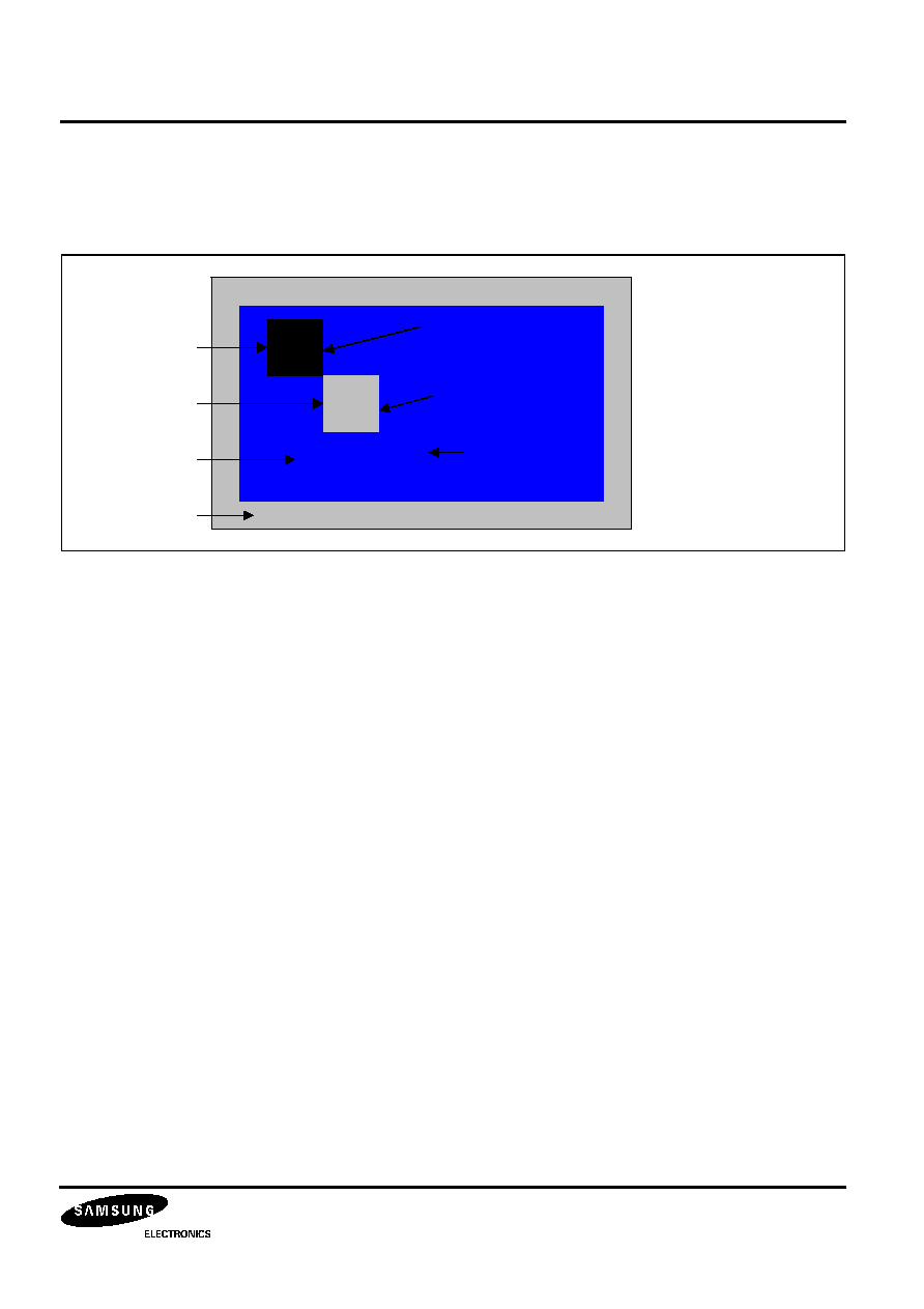
The Frame Control Register 0 'BGEN' bit's function is shown in the Figure below. If you set the 'BGEN' bit as '0'
after selecting A's raster color as black, the raster color black will be displayed. But if you set the 'BGEN' bit as
'1', after selecting B's raster color as black, the raster color black becomes invisible, so the video back ground
color (gray) is displayed as if it is the raster color.
Figure 12. Color Effect by BGEN Bit
BGEN bit = 0 & Rastor Color = Black
BGEN bit = 1 & Rastor Color = Black
BGEN bit = 1 & Rastor Color = Light Blue
C
A
B
Black
Gray
Light Blue
Gray
S1D2514X01 VIDEO AMP MERGED OSD PROCESSOR FOR MONITORS
36
Preliminary
HEIGHT/POSITIONING
∑
Character Height
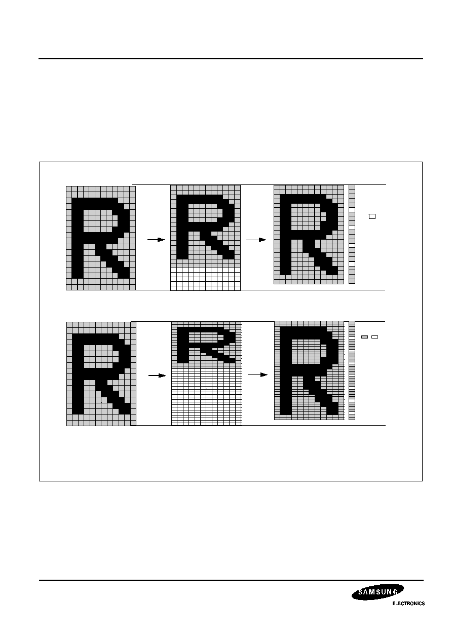
The purpose of CH[5:0] (Character Height) is to output a uniformly sized OSD even if the resolution changes.
To express a Character Height of CH = 18 ~ CH = 63 after receiving CH[5:0]'s input from the frame control
register-1, decide on each line's repeating number (Standard Height CH = 18) and repeat the lines.
The following Figure shows two examples of a height-controlled character. height control is carried out by
repeating some of the lines.
Figure 13. Character Height
Standard Font(12*18)
Standard Font(12*18)
Standard font
in high vertical resolution
Height-controlled font
: added
line
Standard font
in more higher vertical resolution
Height-controlled font
: added
line
1
2
3
4
5
6
7
8
9
10
11
12
13
14
15
16
17
18
1
2
3
4
5
6
7
8
9
10
11
12
13
14
15
16
17
18

VIDEO AMP MERGED OSD PROCESSOR FOR MONITORS
S1D2514X01
37
Preliminary
Repeating line-number can be found by the following formula.
[# of the repeating lines = 2 + N
◊
M],
where N = 1, 2, 3, ... and M = round{14
˜
(CH[5:0]-18)}.
1. If CH[5:0] is greater than 32 and less than or equal to 46 (32 < CH[5:0]
46), all lines are repeated once or
twice. The lines that are repeated twice are chosen by the following formula.
[# of the repeating lines = 2 + N
◊
M],
where N = 1, 2, 3, ... and M = round {14
(CH[5:0]-32)}.
2. If CH[5:0] is greater than 46 and less than or equal to 60 (46 < CH[5:0]
60), all lines are repeated two or three
times. The lines that are repeated three times are chosen by the following formula.
[# of the repeating lines = 2 + N
◊
M],
where N = 1, 2, 3, ... and M = round {14
(CH[5:0]-46)}.
3. If CH[5:0] is greater than 60 and less than or equal to 64 (60 < CH[5:0]
64), all Lines are repeated three or four
times. The lines that are repeated four times are chosen by the following formula.
[# of the repeating lines = 2 + N x M],
where N = 1, 2, 3, ... and M = round {14
(CH[5:0]-60)}.
CH's reference value is 18, and even if you input 0, it operates in the same way as when CH = 18. The repeating
line-number is limited to 16. If the M value is less than or equal to 1, all lines of the standard font are repeated more
than once.
Table 13. Repeating Line as Controlling by CH bits
Character Height
Repeating Line
CH = 18
-
CH = 19
9
CH = 20, 21
6, 13
CH = 22
5, 11, 17
CH = 23
4, 9, 14, 19
CH = 24
3, 7, 11, 15, 19, 21
CH = 25, 26, 27
3, 7, 11, 13, 15, 19, 22
CH = 28
3, 6, 9, 12, 14, 18, 20, 23, 25
CH = 29
3, 6, 9, 11, 13, 15, 18, 21, 23, 25, 26
CH = 30
3, 6, 8, 10, 12, 14, 16, 18, 20, 22, 25, 27
CH = 31
2, 5, 7, 9, 11, 13, 15, 17, 21, 23, 25, 27, 28
CH = 32, 33, 34, 35
2, 5, 7, 9, 11, 13, 15, 18, 21, 23, 25, 27, 28, 29
CH = 36
-
CH = 37
18

S1D2514X01 VIDEO AMP MERGED OSD PROCESSOR FOR MONITORS
38
Preliminary
CH = 38, 39
12, 25
CH = 40
10, 20, 30
CH = 41
8, 16, 24, 32
CH = 42
6, 12, 18, 24, 30, 36
CH = 43, 44, 45
6, 12, 18, 24, 30, 36, 41
CH = 46
4, 8, 12, 17, 21, 25, 29, 33, 37, 41
CH = 47
4, 8, 12, 16, 20, 24, 28, 32, 36, 40, 44
CH = 48
4, 8, 12, 16, 20, 23, 26, 29, 33, 37, 41, 45
CH = 49
4, 8, 12, 16, 19, 22, 25, 28, 31, 35, 39, 43, 47
CH = 50, 51, 52, 53
4, 8, 12, 15, 18, 21, 24, 27, 30, 33, 36, 40, 44, 48
CH = 54
-
CH = 55
27
CH = 56, 57
18, 36
CH = 58
14, 28, 42
CH = 59
12, 23, 34, 45
CH = 60
9, 18, 26, 34, 43, 52
CH = 61, 62, 63
8, 16, 23, 30, 37, 44, 51
Table 13. Repeating Line as Controlling by CH bits
Character Height
Repeating Line (Continued)
VIDEO AMP MERGED OSD PROCESSOR FOR MONITORS
S1D2514X01
39
Preliminary
∑
Positioning
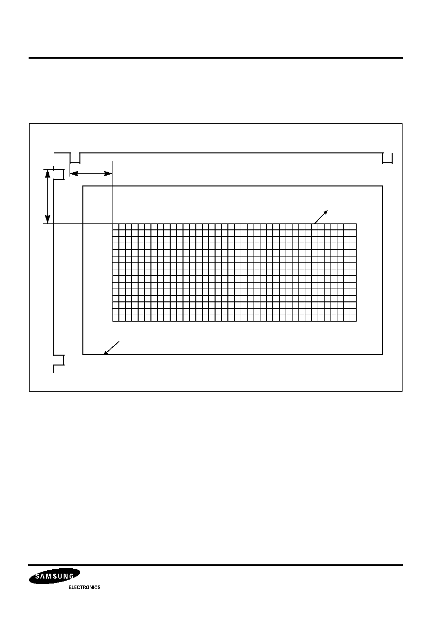
The frame control register-2's HP Bit [F:8] signifies delay of the horizontal display from the H-Sync reference
edge to the character's 1st pixel location, and is controlled by multiplying HP [F:8]'s range value by 6. Also, VP
bit[7:0] signifies the top margin height from the V-Sync reference edge, and is controlled by multiplying 4 to the
VP [7:0]'s range value. Refer to the Figure shown below.
Figure 14. Frame Composition with the OSD Characters
15 rows
(=15 x 18 lines)
HP[7:0]
VP[7:0]
(HFLB)
(VFLB)
Background Screen
30 columns (= 30 x 12 dots)
OSD characters

S1D2514X01 VIDEO AMP MERGED OSD PROCESSOR FOR MONITORS
40
Preliminary
VISUAL EFFECTS
∑
Shadowing
The character shadow can only be black. Character shadow is making 1 pixel to the right and below the
character.
∑
Scrolling
Scrolling is slowly displaying or erasing a character from the top line to the bottom. This effect makes it look as
if 1 character line is scrolling up or down. asharacter line is scrolling up or down.
Figure 15. Character Shadowing
Figure 16. Scrolling
Shadowing

VIDEO AMP MERGED OSD PROCESSOR FOR MONITORS
S1D2514X01
41
Preliminary
PLL CONTROL
∑
Introduction
PLL (Phase Lock Loop) is feedback controlled circuit that maintains a constant phase difference between a
reference signal and an oscillator output signal.
Generally, PLL is composed as follow Figure.
- PFD (Phase Frequency Detector)
PFD compares the phase of the VCO output frequency, with the phase of a reference signal frequency output
pulse is generated in proportion to that phase difference.
- LF (Loop Filter)
LF smooths the output pulse of the phase detector and the resulting DC component is the VCO input.
- VCO (Voltage Controlled Oscillator)
VCO is controlled by loop filter output. The output of the VCO is fed back to the phase frequency detector
input for comparison which in turn controls the VCO oscillating frequency to minimize the phase difference.
- FD (Frequency Divider)
FD divides too much different frequency that is oscillated from the VCO to compare it with reference signal
frequency.
Figure 17. Block Diagram of General PLL
PFD
(Phase Frequency Detector)
LF
(Loop Filter)
VCO (Voltage
Controlled Oscillator)
FD
(Frequency Detector)
Reference Signal

S1D2514X01 VIDEO AMP MERGED OSD PROCESSOR FOR MONITORS
42
Preliminary
∑
PLL of the S1D2514X01
PLL is composed of the phase detector, charge pump, VCO, and N-divider as 4 sub-blocks.
The following is the description of the input/output signals.
- HFLB (Input)
Horizontal flyback signal is refrence signal of the PLL built in S1D2514X01.
The HFLB signal's frequency range is 15 ~ 90kHz, so the PLL block must be a wide range PLL that can cover
HFLB's entire frequency range.
- VCO (Input)
Error signal that passes through an external loop filter is input into VCO.
Operation voltage range is 1-4V. You can raise immunity towards external noise by lowering VCO
sensitivity. You can do this by making it have the maximum operation voltage range possible in the 5V power
voltage.
Figure 18. Block Diagram of the PLL Built in S1D2514X01
Phase
Detector
Charge
Pump
VCO
N-Divider
Loop
Filter
VCO_in
(Pin3)
Div_out
HFLB (Pin32)
CP_out
(Pin4)
VCO_out
CP0
CP1
DOT0
DOT1
HF0 HF1 HF2
# Composed of External Components
fHFLB
< 0.4V
> 4.2V
~2us

VIDEO AMP MERGED OSD PROCESSOR FOR MONITORS
S1D2514X01
43
Preliminary
- DOT0, 1 (Input)
Mode control signal that controls the number of dots per line in the frame control register. There are 4 modes:
320, 480, 640, and 800 dots/line.
According to your choice of mode, the OSD_PLL block's N-Divider is controlled by one of
˜
320,
˜
480,
˜
640, or
˜
800 Divider.
- HF0, 1, 2 (Input)
The horizontal Sync frequency information is received from the micro controller through the frame control
registers-1's bit C-A.
- CP0, 1 (Input)
Charge Pump's output sourcing (or sinking) current control pin.
This control data is received through frame control registers-1's bits E-D.
- VCO_OUT (Output)
VCO output that becomes a system clock. It is the OSD R, G, B output signal's dot frequency, and the standard
signal for OSD's various timings.
Also, it is input into the N-Divider and makes a PLL loop
- CP_OUT (Output)
Charge Pump circuit's output. input into external loop filter. It becomes one of 3 states according to the standard
signal input into the phase detector (HFLB) and the divider output (Div_Out).
- HFLB Div_Out is lead: Current sink
- HFLB Lag: Current source
- HFLB In-Phase: High impedence
fclk
< 0.4V
> 4.2V
Rise Time : < 4nS
Fall Time : < 4nS

S1D2514X01 VIDEO AMP MERGED OSD PROCESSOR FOR MONITORS
44
Preliminary
TUNNING FACTORS OF THE S1D2514X01 PLL
∑
PLL External Circuit
You may follow the recommendations for PCB art work and input/output signal characteristic improvement in
recommendation.
The external circuit that has the most influence on S1D2514X01 PLL block operation is pin 3 (VCO_IN) and pin
4 (CP_OUT)'s surrounding circuit. Refer to OSD PLL block.
Because the PLL circuit is basically a feedback circuit, there are many components that influence the
characteristics. C1, C2, R1, and R2 do not have a localized effect.
As you can see, they are connected to the PLL control bits and influence the characteristics through their
complicated relationships. The main functions of the time canstant and their reference values are as follows.
Figure 19. PLL External Circuit
Table 14. Main Function of Time Constant in PLL External Circuit
Time Canstant
Recommended Value
Main Function
C1
10uF
Influences the damping ratio and controls the PLL
response time
R1
5.6K
(7.5K
)
Same as C1
R2
27K
(or 33K
)
Charge pump current adjustment
C2
33pF
Removes ripple caused by R-C circuit
3
4
R1
R2
C1
C2
1M
5
No Connection
(pin open)

VIDEO AMP MERGED OSD PROCESSOR FOR MONITORS
S1D2514X01
45
Preliminary
∑
PLL Control Bit
After configuring an external circuit using the recommended values, carry out programming using the
recommended values for frequency range and control bits given in the Table below.
(Ref: 800
◊
600, C1: 10uF, R1: 5.6K, R2: 27K, C2: 33pF)
∑
Locking Range
As you can see the figure below, it is 2.35V that measured voltage at pin-3 to optimize OSD quality. The proper
voltage range is 1.5 -- 3.25V.
Table 15. Recommend Values of PLL Control Bit
Register Set
PLL Control Bit
Freq. Range
CP1
CP0
FPLL
HF2
HF1
HF0
DOT1
DOT0
Hex
Below 40kHz
0
0
0
0
1
0
1
1
0B
40 - 50kHz
1
0
0
1
0
0
1
1
93
50 - 70kHz
1
1
0
1
0
1
1
1
A7
Above 70kHz
1
1
0
1
1
1
1
1
AF
Figure 20. Locking Range
1.625V
fmax
f0
-2
•
1.625V
2
•
fL
fC
Locking Range
Ve (min)
Ve (max)
0.75V
1.5V
2.37V
3.25V
4V
S1D2514X01 VIDEO AMP MERGED OSD PROCESSOR FOR MONITORS
46
Preliminary
∑
HF Bits Selection
HF bits is not selecting from out of 8 (2
3
) steps uniformly, but selecting the step shown in figure below. In
example, at 800 mode, there are 5 steps that the frequency range is controlled by HF bits.
After fixing time constants of the external circuit and PLL control bits except HF bits, if HF bits are stepped up, the
voltage measured at pin-3 drops. On the contrary, if HF bits are stepped down, the voltage rises.
The voltage measured at pin-3 don't change by changing CP bits.
∑
External Register at pin-4
The external register at pin-4 is the factor that changes greatly at PLL tunning. The initial value of this external
register value is decided as follows.
At first, the external register is replaced variable-register (about 50K
range).
and then, set the lowest PLL control bits at the lowest frequency allowed by set.
and then, change variable-register to be 2.35V that optimum voltage is locking.
and then, measure register value at this time.
also, set the highest PLL control bits at the highest frequency allowed by set.
and then, change variable-register to be 2.35V that optimum voltage is locking.
and then, measure register value at this time.
You may decide the average of these two registers' value to initial value.
Table 16. HF Bits Selection
DIV
DOT1
DOT0
HF2
HF1
HF0
320
0
0
480
0
1
640
1
0
800
1
1

VIDEO AMP MERGED OSD PROCESSOR FOR MONITORS
S1D2514X01
47
Preliminary
The table below shows that other factors change as changing external register's value.
Fixing Factor
Variable Factor
Change
Voltage
Current
Lock Range
Time constants of the external circuit
and PLL control bits except
Rext
(shift)
(shift)

S1D2514X01 VIDEO AMP MERGED OSD PROCESSOR FOR MONITORS
48
Preliminary
RECOMMENDATION
5V Power Routing
S1D2514X01's OSD part power is composed of analog VDD and digital VDD. To eliminate clock noise influence in
the digital block, you need to separate the analog VDDA and digital VDD.
(BD102 use: Refer to Application Circuit )
12V Power Routing
Because S1D2514X01 is a wideband AMP of above 150MHz, 12V power significantly affects the video
characteristics. The effects from the inductance and capacitance are different for each board, and , therefore,
some tuning is required to obtain the optimum performance. The output power, VCC2, must be separated from
VCC1 and VCC3 using a coil, which is parallel-connected to the damping resistor.The appropriate coil value is
between 20uH - 200uH. Parallel-connected a variable resistor to the coil and control its resistance to obtain the
optimum video waveform.
(Moreover, BD103 can tune using a coil and variable resistor to obtain the optimum video waveform.
L103, R124, BD103: Refer to application circuit)
VCC1, VCC3 12V Power
Use a 104 capacitor and large capacitor greater than 470uH for the power filter capacitor.
12V Output Stage Power VCC2
Do not use the power filter capacitor.
5V Digital Power VDD
Don't use a coil or magnetic core to the VDD input. Make the power filter capacitor, an electric capacitor of greater
than 50uF, single and connect it to VSS, the digital GND.
Output Stage GND2
Care must be taken during routing because it ,as an AMP output stage GND, is an important factor of video
oscillation. R/G/B clamp cap and R/G/B load resistor must be placed as close as possible to the GND2 pin. GND2
must be arranged so that it has the minimum GND loop, which at one point must be connected to the main GND.
Digital GND VSS
When this is to be connected directly to the GND2, it can cause the OSD clock noise, so the loop connection
should be routed as far away as possible. If the OSD clock noise affects the screen, separate VSS GND from all
GND and connect it to the main board using a bead. Again, the bead connection point should be placed as far
away as possible to the GND2.
Analog Block
The PLL built in to S1D2514X01 is sensitive to noise due to the wide range PLL characteristics. Therefore, you
need to isolate the analog block in the following manner. First make a separate land for the analog block (pin2 -
pin6)'s ground, and connect it to the main ground through a 1M
resistor. The analog GND of both sides of a
double faced PCB must be separated from the main ground. (Separate pin 2's 5V analog GND, which is the GND
for OSD PLL, from the main and digital GNDs and connect it to the main GND using about 1M
resistor. GND for
pins 2 - 6 is the No. 2 VSSA GND.)

VIDEO AMP MERGED OSD PROCESSOR FOR MONITORS
S1D2514X01
49
Preliminary
I
2
C Control Line (SCL, SDA Line)
I
2
C communication noise (noise generated in the OSD display pattern when data is transmitted in the I
2
C line) may
be generated because of an I
2
C control line that passes near the analog block. The I
2
C control lines near
S1D2514X01 must be separated from the analog block as much as possible.
Furthermore, the I
2
C bus interference can be prevented by inserting a series resistor in the line.
Horizontal Flyback Signal
Display jittering can be generated if the horizontal signal (HFLB) input to S1D2514X01 is not a clean signal.
We recommend a short path and shielded cable for obtaining a clean signal.
Generally, the input horizontal signal (HFLB) is generated by using a high voltage horizontal flyback signal. The
effect from the high voltage flyback signal can be reduced by separating the R115 and R117 GND, which
determines the flyback signal slice level, from the transistor GND, which generates the actual S1D2514X01 input
horizontal signal. Furthermore, the flyback signal sharpness must be maintained by minimizing the values of R115,
R116 and R117 resistors, which set the horizontal signal slice level. values.
(R115, R116, R117: Refer to application circuit )
HFLB Input Signal Generator
You can correct the circuit by reducing the resistors that sets the slice level of the horizontal signal in the HFLB-
generating circuit.
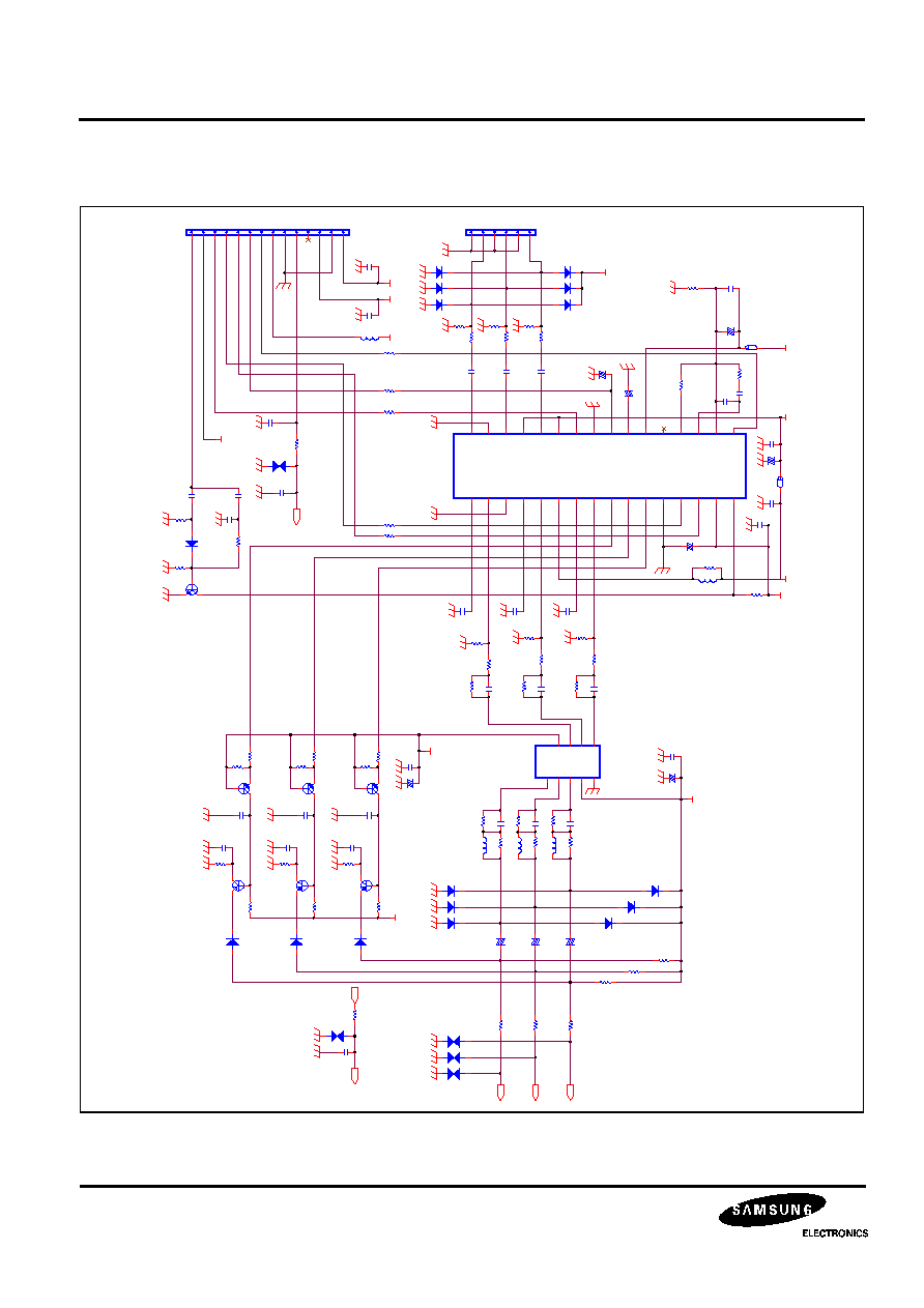
S1D2514X01 VIDEO AMP MERGED OSD PROCESSOR FOR MONITORS
50
Preliminary
APPLICATION BOARD CIRCUIT
Figure 21. Application Board Circuit
5V
12V
70V
5V
70V
12V
6.3V
12_1V
5V
70V
12V
12V
RB15
47
C108
47uF
+
DB03
1SS244
CN1
1
2
3
4
5
6
C109
103
C114
33pF
R123
1M
R109
27K
R107
1K
R102
100
C116
1nF
CR01
104
CG02
104
CB02
104
L101
100uH
R118
560
R119
560
DR05
1N4148
CG05
104
DG05
1N4148
CB05
104
CB05
104
QB02
2N5401C-Y
2
1
3
DB05
1N4148
RG15
47
RR15
47
CB04
1uF
+
DG03
1SS244
DR03
1SS244
RR09
75K
RG09
75K
RB09
75K
RB10
39
CG04
1uF
+
RG10
39
CR04
1uF
+
DB04
1SS244
DG04
1SS244
DR04
1SS244
RG02
75
D102
1N4148
RR02
75
DB01
1N4148
QR01
2N5551C-Y
2
1
3
R116
10K
BD102
QB01
2N5551C-Y
2
1
3
Q102
2N3904
2
1
3
CR05
104
QR02
2N5401C-Y
2
1
3
RB13
82K
R103
390
DRIVER IC
BIN
6
ROUT
1
GOUT
2
GIN
7
GND
5
RIN
9
VBB
8
BOUT
3
VCC
4
RB02
75
C117
1nF
QG01
2N5551C-Y
2
1
3
CR05
104
R101
4.7K
C110
100uF
+
QG02
2N5401C-Y
2
1
3
RG11
100
RB11
100
CN2
1
2
3
4
5
6
7
8
9
10
11
12
13
14
CG05
104
RR11
100
C112
1uF
+
C123
103
DG02
1N4148
CG02
104
RG13
82K
SKB01
DMS-200D
C128
104
CB02
104
RB03
470
SKR01
DMS-200D
CR02
104
SKG01
DMS-200D
DR02
1N4148
C107
220uF
+
C160
47uF
+
R114
470
C121
104
RR01
75
RR03
470
RR12
2.2K
RG12
2.2K
RB12
2.2K
RB01
75
C124
103
C119
102
R117
150
DB02
1N4148
C102
1uF
+
R115
2K
RG03
470
C118
330pF
RG01
75
RR13
82K
SK101
WSP-401M
C152
104
C103
470uF
+
BD103
C126
1.8nF
SK102
DMS-200D
C120
1nF
R104
390
C113
10uF
R108
5.6K
DG01
1N4148
C151
104
RB20
4.7K
DR01
1N4148
RR20
4.7K
KB2514
VFLB
1
VSSA
2
VCO_IN
3
VREF1
4
VREF
5
VDDA
6
CONT_CAP
7
ABL_IN
8
GND
9
CLP_IN
10
VCC3
11
RIN
12
VCC1
13
GIN
14
GND1
15
BIN
16
BCLP
17
BOUT
18
GND2
19
GCLP
20
GOUT
21
VCC2
22
RCLP
23
ROUT
24
BCT
25
GCT
26
RCT
27
VSS
28
SCL
29
SDA
30
VDD
31
HFLB
32
C106
104
RG20
4.7K
R124
220
L103
27uH
RB04
100
CB08
270pF
RG04
100
CG08
270pF
RR04
100
CR08
270pF
RB08
56
CB07
37pF
RG08
56
CG07
37pF
RR08
56
CR07
37pF
RB14
75
RG14
75
RR14
75
LB01
0.15uH
LG01
0.15uH
LR01
0.15uH
RR10
39
B_OUT
G_OUT
R_OUT
G1
G2
G2

VIDEO AMP MERGED OSD PROCESSOR FOR MONITORS
S1D2514X01
51
Preliminary
TYPICAL APPLICATION CIRCUIT
Figure 22. Typical Application Circuit
5V
12V
70V
5V
70V
12V
6.3V
12_1V
5V
70V
12V
12V
RB15
47
C108
47uF
+
DB03
1SS244
CN1
1
2
3
4
5
6
C109
103
R123
1M
R109
27K
R107
1K
R102
100
C116
1nF
CR01
104
CG02
104
CB02
104
L101
100uH
R118
560
R119
560
DR05
1N4148
CG05
104
DG05
1N4148
CB05
104
CB05
104
QB02
2N5401C-Y
2
1
3
DB05
1N4148
RG15
47
RR15
47
RB14
75
LB01
0.15uH
CB04
1uF
+
DG03
1SS244
DR03
1SS244
RR09
75K
RG09
75K
RB09
75K
RB10
39
RG14
75
LG01
0.15uH
CG04
1uF
+
RG10
39
RR14
75
LR01
0.15uH
CR04
1uF
+
RR10
39
DB04
1SS244
DG04
1SS244
DR04
1SS244
RG02
75
D102
1N4148
RR02
75
DB01
1N4148
QR01
2N5551C-Y
2
1
3
R116
10K
BD102
QB01
2N5551C-Y
2
1
3
Q102
2N3904
2
1
3
CR05
104
QR02
2N5401C-Y
2
1
3
RB13
82K
R103
390
DRIVER IC
BIN
6
ROUT
1
GOUT
2
GIN
7
GND
5
RIN
9
VBB
8
BOUT
3
VCC
4
RB02
75
C117
1nF
QG01
2N5551C-Y
2
1
3
CR05
104
R101
4.7K
C110
100uF
+
QG02
2N5401C-Y
2
1
3
RG11
100
RB11
100
CN2
1
2
3
4
5
6
7
8
9
10
11
12
13
14
CG05
104
RR11
100
C112
1uF
+
C123
103
DG02
1N4148
CG02
104
RG13
82K
SKB01
DMS-200D
C128
104
CB02
104
RB03
470
SKR01
DMS-200D
CR02
104
SKG01
DMS-200D
DR02
1N4148
C107
220uF
+
C160
47uF
+
R114
470
C121
104
RR01
75
RR03
470
RR12
2.2K
RG12
2.2K
RB12
2.2K
RB01
75
C124
103
C119
102
R117
150
DB02
1N4148
C102
1uF
+
R115
2K
RG03
470
C118
330pF
RG01
75
RR13
82K
SK101
WSP-401M
C152
104
C103
470uF
+
BD103
C126
1.8nF
SK102
DMS-200D
C120
1nF
R104
390
C113
10uF
R108
5.6K
DG01
1N4148
C151
104
RB20
4.7K
DR01
1N4148
RR20
4.7K
KB2514
VFLB
1
VSSA
2
VCO_IN
3
VREF1
4
VREF
5
VDDA
6
CONT_CAP
7
ABL_IN
8
GND
9
CLP_IN
10
VCC3
11
RIN
12
VCC1
13
GIN
14
GND1
15
BIN
16
BCLP
17
BOUT
18
GND2
19
GCLP
20
GOUT
21
VCC2
22
RCLP
23
ROUT
24
BCT
25
GCT
26
RCT
27
VSS
28
SCL
29
SDA
30
VDD
31
HFLB
32
C106
104
RG20
4.7K
R124
220
L103
27uH
C114
33pF
B_OUT
G_OUT
R_OUT
G1
G2
G2

S1D2514X01 VIDEO AMP MERGED OSD PROCESSOR FOR MONITORS
52
Preliminary
ROM FONTS
Figure 23. ROM Fonts

VIDEO AMP MERGED OSD PROCESSOR FOR MONITORS
S1D2514X01
53
Preliminary