
DECEMBER. 2001
Ver 2.1
DATA SHEET
S1D2518X01
Preliminary
I
2
C BUS CONTROLLED R/G/B VIDEO AMPLIFIER FOR MONITORS S1D2518X01
1
Preliminary
I
2
C BUS CONTROLLED R/G/B VIDEO AMPLIFIER
The S1D2518X01 is a high frequency video amplifier system with I
2
C
bus control used in monitors.
It contains 3 matched R/G/B video amplifiers with OSD interface and
provides flexible interfacing to I
2
C bus controlled adjustment systems.
FUNCTIONS
∑
I
2
C bus controlled 150MHz RGB video pre-amplifier for monitors
∑
The S1D2518X01 is a high frequency video amplifier system with OSD interface controlled by I
2
C bus.
∑
All controls and adjustments are digitally performed thanks to I
2
C bus.
: Contrast, brightness and DC output level of R/G/B signals common to the 3-channel and drive adjustment
(sub contrast), cut-off control are separated for each channel.
∑
The S1D2518X01 is included video & OSD half tone function.
∑
The white balance adjustment is effective on brightness, video & OSD signals.
∑
The S1D2518X01 works for application using AC coupled CRT driver.
∑
In addition to beam current limitation (ABL), OSD intensity interface is possible with external pins.
ORDERING INFORMATION
FEATURES
∑
3-channel matched R/G/B Video Amplifier
∑
I
2
C BUS control items
- Contrast control
- Brightness control
- SUB contrast control for each channel
- OSD contrast control
- Cut-off control for each channel
- Brightness control for cut-off
- Switch registers for SBLK, half tone,
NSS (No Signal Switch: Blank video signal except
OSD signal)
and CPS (Clamp Pulse Input Polarity Selection).
∑
Built in clamp gate with anti OSD sagging
∑
Built in OSD Interface, OSD BLK
∑
Built in OSD Intensity Interface
∑
Built in ABL (Automatic Beam Limitation)
Device
Package
Operating Temperature
S1D2518X01
30-SDIP-400
-25 to +75
∞
∞
∞
∞
C
30-SDIP-400
∑
Built in video input clamp, BRT clamp
∑
Built in video & OSD half tone function on OSD
picture.
∑
3-channel R/G/B video amplifier 150MHz
@f-3dB
∑
TTL OSD inputs, 80MHz bandwidth
∑
Contrast control range: 38dB
∑
SUB contrast control range: 11dB
∑
OSD contrast control range: 38dB
∑
Capable of 7Vp-p output swing
∑
High speed OSD BLK
∑
Single DAC output

S1D2518X01 I
2
C BUS CONTROLLED R/G/B VIDEO AMPLIFIER FOR MONITORS
2
Preliminary
BLOCK DIAGRAM
Figure 1. Block Diagram
Interface & Control
1
2
3
9
5
6
7
8
30
12
4
20
10
21
11
VI/
OSD_SW
OSD
Interface
CLPB
Video
OSD
Switch
OSD
Contrast
Video
Contrast
+
SUB
Contrast
ROSD
GOSD
BOSD
VCC3
RIN
VCC1
GND1
GIN
INT
ABL
CLP
BIN
BLK
GND3
gm1
gm2
28
29
19
25
24
23
25
22
17
26
27
18
14
13
+
BLKB
CLPB
OSD
Intensity
ABL
Clamp
Gate
Video/OSD
Switch
Blank
Gate
HALF-TONE
Control
CLPB BLKB
I
2
C Bus Control
Cut Off Bright (06H)
ROUT
RCLP
RCT
VCC
GND
BOUT
BCLP
BCT
GOUT
GCLP
SDA
SCL
GCT
Cut Off Bright Offset (D5, D6 : 01H)
R/G/B Cut Off Control (07/08/09H)
Brightness Control (01H)
R/G/B Drive Control (02/03/04H)
OSD Cont Control (05H)
Contrast Contral (00H)
16
DAC OUT
IS 1/2 (D1, D2: 0AH)
Soft Blank
(D7 : 01H)
Clamp Polarity Select D3 (0BH)
One (red)
Of Three Channels
+
1.9V
Main
Amp
HT (D0 : 0AH)
No Signal
Control
15
VDD
I
2
C BUS CONTROLLED R/G/B VIDEO AMPLIFIER FOR MONITORS S1D2518X01
3
Preliminary
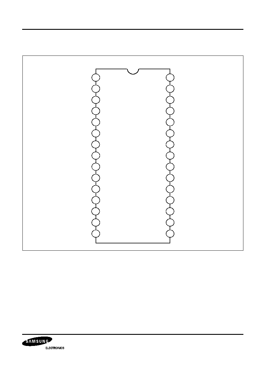
PIN CONFIGURATION
Figure 2. Pin Configuration
S1D2518X01
1
2
3
4
5
6
7
8
10
9
11
12
13
14
15
30
29
28
27
26
25
24
23
21
22
20
19
18
17
16
ROSD
GOSD
BOSD
VI/
OSD_SW
RIN
VCC1
GND1
GIN
BIN
VCC3
GND3
ABL
SCL
SDA
VDD
INT
RCLP
ROUT
GCLP
GOUT
VCC2
GND2
BOUT
BLK
BCLP
CLP
RCT
GCT
BCT
DAC OUT

S1D2518X01 I
2
C BUS CONTROLLED R/G/B VIDEO AMPLIFIER FOR MONITORS
4
Preliminary
Table 1. Pin Configuration (continued)
Pin No
Symbol
I/O
Configuration
1
ROSD
I
Red OSD input
2
GOSD
I
Green OSD input
3
BOSD
I
Blue OSD input
4
VI/OSD_SW
I
Video or OSD switch
5
RIN
I
Red video input
6
VCC1
-
VCC (normal)
7
GND1
-
Ground1 (normal)
8
GIN
I
Green video input
9
VCC3
-
VCC (logic)
10
BIN
I
Blue video input
11
GND3
-
Ground (logic)
12
ABL
I
Automatic beam limit
13
SCL
I/O
Serial clock
14
SDA
I/O
Serial data
15
VDD
-
5V VDD
16
DAC OUT
O
DAC output
17
BCT
I
Blue cut off control
18
GCT
I
Green cut off control
19
RCT
I
Red cut off control
20
CLP
I
Clamp gate signal input
21
BLK
I
Blank gate signal input
22
BCLP
-
Blue clamp cap
23
BOUT
O
Blue video output
24
GND2
-
Ground2 (drive part)
25
VCC2
-
VCC (drive part)
26
GOUT
O
Green video output
27
GCLP
-
Green clamp cap
28
ROUT
O
Red video output
29
RCLP
-
Red clamp cap
30
INT
I
OSD intensity
I
2
C BUS CONTROLLED R/G/B VIDEO AMPLIFIER FOR MONITORS S1D2518X01
5
Preliminary
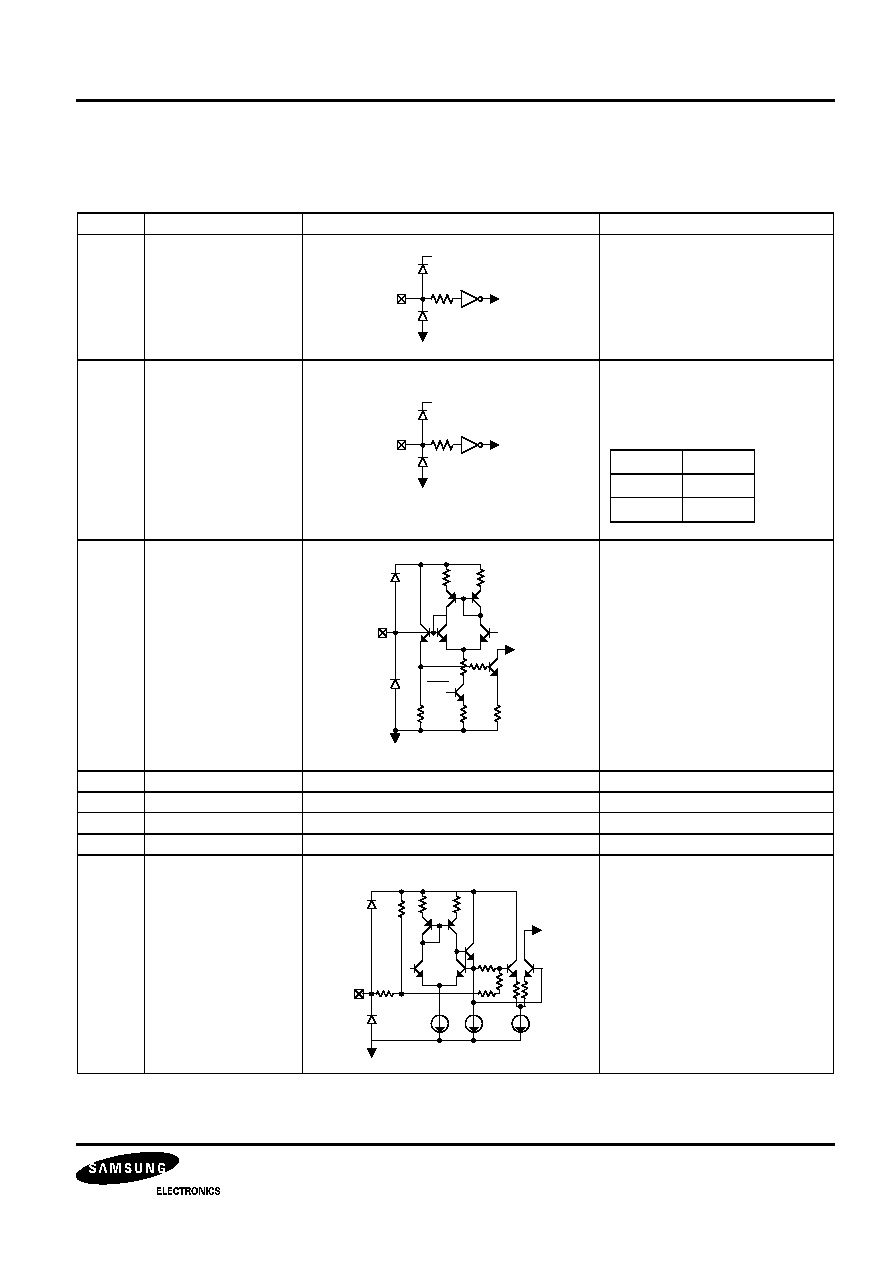
PIN DESCRIPTION
Table 2. Pin Description
Pin No
Pin Name
Schematic
Description
1
2
3
Red OSD input
(ROSD)
Green OSD input
(GOSD)
Blue OSD input
(BOSD)
OSD input signals are in TTL
level and will be connected to
ground when switching to video
input
4
Video/OSD switch
(VI/OSD_SW)
Video/OSD signal is switched by
pin4 DC level
PIN4 = "High", OSD input
PIN4 = "Low", video input
5
8
10
Red video input
(RIN)
Green video input
(GIN)
Blue video input
(BIN)
MAX input video signal is 1.2Vpp
6
VCC1
-
Normal power supply (12V)
7
GND1
-
Normal ground
9
VCC3
-
Logic power supply
11
GND3
-
Logic ground
12
ABL
Auto beam limitation input
(control range: 0.5 to 4.5V)
5V
0.224K
5V
0.224K
Pin4
Output
High
OSD
Low
Video
1.9V
12V
CLP
12V
100K
2.5V
0.3K

S1D2518X01 I
2
C BUS CONTROLLED R/G/B VIDEO AMPLIFIER FOR MONITORS
6
Preliminary
13
Serial clock input
(SCL)
SCL for I
2
C bus control
14
Serial data input
(SDA)
SDA for I
2
C bus control
15
VDD
-
Logic power supply (5V)
16
DAC OUT
8-bit DAC current output.
The 8-bit DAC controls the
sinking current amounts from 0 to
500uA.
If you want a voltage output, you
must use the pull-up resistor.
This pin function is similiar with
pin 17, 18, 19.
17
18
19
Blue cut-off control
(BCT)
Green cut-off control
(GCT)
Red cut-off control
(RCT)
Cut-off control output
Table 2. Pin Description (Continued)
Pin No
Pin Name
Schematic
Description
5V
0.224K
5V
0.224K
ack
12V
0-200uA
0-500uA
90uA
170uA
12V
Cut-off
BRT
Cut
-off
CS1 CS2
CTX

I
2
C BUS CONTROLLED R/G/B VIDEO AMPLIFIER FOR MONITORS S1D2518X01
7
Preliminary
20
Clamp gate input
(CLP)
The Video amp actives when
clamp gate signal is in low/high
TTL level.
Clamp gate min. pulse width
: 0.2us, at fh: 50kHz
21
Blank gate input
(BLK)
The video amp blanks video
signal when blank gate signal is
the positve HFLB signal or
positve TTL signal.
29
27
22
Red clamp cap
(RCLP)
Green clamp cap
(GCLP)
Blue clamp cap
(BCLP)
The Brightness (pedestal) control
is activated by charging and
discharging of the external cap.
(0.1
µ
F)
(During clamp gate)
28
26
23
Red video output
(ROUT)
Green video output
(GOUT)
Blue video output
(BOUT)
Video signal output
24
GND2
-
Drive ground
25
VCC2
-
Drive power supply (12V)
30
OSD intensity input
(INT)
Active high (TTL level)
Table 2. Pin Description (Continued)
Pin No
Pin Name
Schematic
Description
5V
0.224K
CPS Bit
CLP Signal
0
Low
1
High
5V
0.224K
5V
10K
12V
0.3K
Ext. CAP
lclamp
12V
20
40
0.224K
5V
INT Input
OSD Intensity
High
ON
Low
OFF
S1D2518X01 I
2
C BUS CONTROLLED R/G/B VIDEO AMPLIFIER FOR MONITORS
8
Preliminary
ABSOLUTE MAXIMUM RATING (TA = 25
∞
∞
∞
∞
C)
(see 1)
RECOMMENDED OPERATIONS CONDITIONS
THERMAL & ESD PARAMETER
Table 3. Absolute Maximum Rating
No
Item
Symbol
Value
Unit
Min
Typ
Max
1
Maximum supply voltage
V
CC
1/2/3
-
-
15
V
2
Operating temperature
(see 2)
Topr
-25
-
75
∞
C
3
Storage temperature
Tstg
-65
-
150
∞
C
4
Power dissipation
P
D
-
-
1.2
W
5
Logic part power supply
V
DD
-
-
6
V
Table 4. Recommended Operations Conditions
No
Item
Symbol
Value
Unit
Min
Typ
Max
1
Operating supply voltage
V
CCOP
11.4
12.0
12.6
V
(see 3)
2
Operating supply voltage
V
DD
V
DDOP
4.75
5.0
5.25
V
Table 5. Thermal & ESD Parameter
No
Item
Symbol
Value
Unit
Min
Typ
Max
1
Thermal resistance
(junction-ambient)
ja
-
62
-
∞
C/W
2
Junction temperature
Tj
-
150
-
∞
C
3
Human body model
(C = 100p, R = 1.5k)
HBM
±
2
-
-
KV
4
Machine model
(C = 200p, R = 0)
MM
±
200
-
-
V
5
Charge device model
CDM
±
800
-
-
V

I
2
C BUS CONTROLLED R/G/B VIDEO AMPLIFIER FOR MONITORS S1D2518X01
9
Preliminary
ELECTRICAL CHARACTERISTICS
DC ELECTRICAL CHARACTERISTICS
Ta = 25
∞
C, V
CC1
= V
CC2
= V
CC3
= 12V, V
DD
= 5V; Pin1, 2, 3, 4 = 0V; Pin20=4V; Pin30 = 0V; POR;
unless otherwise stated
Table 6. DC Electrical Characteristics
Parameter
Symbol
Conditions
Min
Typ
Max
Unit
Supply current
I
CC
(see 4)
50
65
80
mA
Maximum supply current
ICCmax
V
CC1, 2, 3
= 15V
100
140
180
mA
Video input bias voltage
Vbias
1.6
1.9
2.2
V
Clamp gate low input voltage
V22L
P
20
= 4V
0V
1.0
1.5
2.0
V
Clamp gate high input voltage
V22H
P
20
= 0V
4V
1.0
1.5
2.0
V
Clamp gate low input current
I22L
-8
-4
-
uA
Clamp gate high input current
I22H
P
20
= 12V
-
3
6
uA
Clamp cap charge current
Iclamp+
P
22, 27, 29
= 4V
0.4
0.8
1.2
m
Clamp cap discharge current
Iclamp-
P
22, 27, 29
= 8V
-1.2
-0.8
-0.4
m
Blank gate low input voltage
V23L
P
21
= 4V
0V
0.6
0.7
-
V
Blank gate high input voltage
V23H
P
21
= 0V
4V
0.6
0.7
-
V
Blank gate low input current
I23L
P
21
= 0V
-8
-4
-
uA
Blank gate high input current
I23H
P
21
= 12V
-
3
6
uA
BRT output voltage (POR)
VOpor
P
20
= S8 (pulse width 0.2us/38kHz)
0.3
0.6
0.9
V
Black level voltage channel
difference
VO
BL
(see 5)
-
-
0.3
V
Clamp cap high voltage
V_CLP
V
CC1, 2, 3
= 15V
8
10
12
V
Video output high voltage
VOH
P
20
= 4V
6.2
7.5
9
V
Video blank output voltage
VOB
-
0.1
0.3
V
SCL high input current
I13H
-
0.01
1
uA
SDA high input current
I14H
-
0.01
1
uA
SCL/SDA low level input voltage
VbusL
OB: O/H, SCL/SDA signal
high = 3.5V, low = 1.5V
-
-
1.5
V
SCL/SDA high level input
voltage
VbusH
3.5
-
-
V
SCL/SDA input pin ref. voltage
VbusR
P
13, 14
= open status
1.5
2.0
2.5
V
Video input resistance
VIDEOin
10
100
-
k
Spot killer voltage
Vspot
V
CC1, 2, 3
= 12
9V
10.0
10.7
11.4
V
POR ext. cut-off output current
IctXpo
150
250
350
uA
Cut-off min. output voltage
difference
Vcutmin
Vcutmin = Vout [07, 08, 09: 00H] -
Vout [POR]
-0.6
-0.4
-0.2
V
Cut-off max. output voltage
difference
Vcutmax
Vcutmax = Vout [07, 08, 09: FFH] -
Vout [POR]
0.2
0.4
0.6
V

S1D2518X01 I
2
C BUS CONTROLLED R/G/B VIDEO AMPLIFIER FOR MONITORS
10
Preliminary
Ext. cut-off output current range
Ictx
P
17, 18, 19
= 5V,
Ictx = P18's I [07, 08, 09: FFH] -
P18's I [07, 08, 09: 00H]
330
480
630
uA
Cut-off BRT output current range
Ictbrt
P
17, 18, 19
= 5V,
Ictbrt = P18's I [06:FFH] - P18's I
[06:00H]
130
200
330
uA
Ext. cut-off offset output current1
Ics1
P
17, 18, 19
= 5V, 06 - 09: 00H, CS1
bit = 1
100
140
180
uA
Ext. cut-off offset output current2
Ics2
P
17, 18, 19
= 5V, 06 - 09: 00H, CS2
bit = 1
160
240
320
uA
Video soft blank output voltage
VOsoft
SBLK bit = 1
-
0.1
0.3
V
Wrong slave address det.
WSADDR
when wrong slave address is
inputted you must measure voltage.
-
0.1
0.3
V
Blank polarity selector voltage
VBPS
BPS bit = 1
-
0.1
0.2
V
Clamp polarity selector voltage
VCPS
CPS bit = 1
0.9
1.4
1.9
V
Video brightness low output
voltage
VOBL
01: 00H
0.3
0.6
0.9
V
Video output worst low output
VLOW
-0.2
-
0.2
V
Video brightness high output
voltage
VOBH
01: 1FH
1.3
1.8
2.3
V
Max. output voltage
Vmax
6.5
8.0
9.5
V
Table 6. DC Electrical Characteristics (Continued)
Parameter
Symbol
Conditions
Min
Typ
Max
Unit
I
2
C BUS CONTROLLED R/G/B VIDEO AMPLIFIER FOR MONITORS S1D2518X01
11
Preliminary
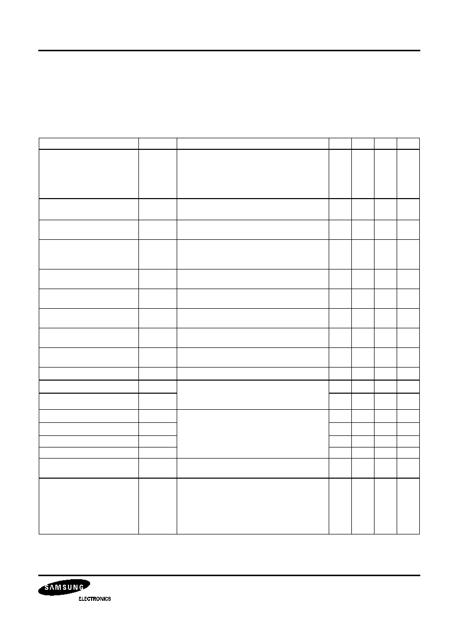
AC ELECTRICAL CHARACTERISTICS
Ta
= 25
∞
C, V
CC1
= V
CC2
= V
CC3
=12V, V
DD
= 5V; Pin1, 2, 3, 4 = 0V; Pin5, 8, 10 = S1; Pin21 = 4V; Pin20 = S8;
Pin30 = 0V; POR.
Vin = 0.56Vpp manually adjust video output pins 23, 26 and 28 to 4V DC for the AC test
(see 11)
unless otherwise
stated
(see 12)
Table 7. AC Electrical Characteristics
Parameter
Symbol
Conditions
Min
Typ
Max
Unit
Video bandwidth
(see 7,8)
f -3dB
P
5, 8, 10
= S2, 00, 02, 03, 04 = FFH
When P
20
= 0V, you must measure clamp cap
pin voltage.
Then P
20
= 4V, P
8
= 2.2V, clamp cap pin =
above measurement voltage.
150
-
MHz
Video amp gain
AVmax
P
20
= S8 (low: 0.5V, high: 3V) 00, 02, 03, 04 =
FFH
16
18
20
dB
Max. gain channel difference
AVmax
(see 6,7)
AVmax = 20log (Vout / Vin)
AVmax =20log (Voutch1 / Vontch2)
-
-
1
dB
Low gain channel difference
AVlow
(see 6,7)
P
20
= S8 (low: 0.5V, high: 3V), 00 = 40H, 02, 03,
04 = FFH
AVlow = 20log (Voutch1 / Voutch2)
-
-
1
dB
Sub drive ctrl max-center
AVDmax
AVDmax = 20log (Vout [02, 03, 04: 80H]/ Vout
[02, 03, 04: FFH])
-6
-4
-2
dB
Sub drive ctrl min-center
AVDmin
AVDmin = 20log (Vout [02, 03, 04: 00H]/ Vout
[02, 03, 04: 80H])
-10.5
-7.5
-4.5
dB
Contrast ctrl max-center
AVCmax
AVCmax = 20log (Vout [02, 03, 04: 80H]/ Vout
[02, 03, 04: FFH])
-6.5
-4.5
-2.5
dB
Contrast ctrl min-center
AVCmin
AVCmin = 20log (Vout [00:00H] / Vout [00, 02,
03, 04: 80H])
-
-
-35
dB
ABL control range
ABL
00, 02, 03, 04 = FFH,
ABL = 20log
(Vlow [P12 = 0.5V] / Vmax [P12 = 5V])
-13
-10
-7
dB
Video amp THD
THD
P
5, 8, 10
= S5, P20 = 4V, P
22, 27, 29
= Var.
-
1
5
%
Video rising time
(see 7)
tr
P
5, 8, 10
= S6, Pedestal Level = over 1V.
Decreasing the output load resistor makes the
rise/fall time faster.
-
-
2.7
nS
Video falling time
(see 7)
tf
-
-
2.7
nS
Blank output rising time
(see 7)
trBlank
P
20
= 0V, P
21
= S7
-
-
10
nS
Blank output falling time
(see 7)
tfBlank
-
-
10
nS
Blank rising prop. delay
trBlankPr
-
25
35
nS
Blank falling prop. delay
tfBlankPr
-
15
25
nS
Video output channel crosstalk
10kHz
CT_10K
(see 9)
P
5
= S3, P
20
= 4V, 00, 02, 03, 04: FFH
-
-
-45
dB
Video output channel crosstalk
10MHz
CT_10M
(see 7,9)
When P
20
= 0V, you must measure clamp cap
pin voltage.
Then P
20
= 4V, video input pin = 2.2V DC bias,
clamp cap pin = above measurement voltage
CT-10K = 20log (Voutch2 / Voutch2 [AVmax
Vout])
-
-
-35
dB

S1D2518X01 I
2
C BUS CONTROLLED R/G/B VIDEO AMPLIFIER FOR MONITORS
12
Preliminary
OSD ELECTRICAL CHARACTERISTICS
Ta = 25 ∞C, V
CC1
= V
CC2
= V
CC3
= 12V, V
DD
= 5V;
Pin1, 2, 3, 4 = 4V; Pin21 = 4V; Pin12, 20, 30 = 0V; POR; unless otherwise stated
Table 8. OSD Electrical Characteristics
Parameter
Symbol
Conditions
Min
Typ
Max
Unit
OSD low input voltage
V
OSD
L
P
4
= S7, P
1, 2, 3
= 4V
0V
2.0
2.5
3.0
V
OSD high input voltage
V
OSD
H
P
4
= S7, P
1, 2, 3
= 0V
4V
2.0
2.5
3.0
V
OSD select low input voltage
VosdsL
P
4
= S7 (S7's level 5Vpp
0Vpp)
2.0
2.5
3.0
V
OSD select high input voltage
VosdsH
P
4
= S7 (S7's level 0Vpp
5Vpp)
2.0
2.5
3.0
V
OSD Max. output voltage
Vosd
P
1, 2, 3
= 3V, P
4
= S7, 05: FFH
3
4
5
V
PP
OSD Max. gain channel
difference
Vosd
P
1, 2, 3
= 3V, P
4
= S7, 05: FFH,
Vosd = Vosdch1 - Vosdch2
-
-
500
mVpp
OSD attenuation
Vosdatt
P
1, 2, 3
= 3V, P
4
= S7, Vosdatt =
Vosd [05:80H] / Vosd [05:FFH]
◊
100
30
50
70
%
OSD center output voltage
Vosdc
P
1, 2, 3
= 3V, P
4
= S7, 05: 80H
1.7
2.4
3.1
Vpp
OSD center gain channel
difference
VosdC
P
1, 2, 3
= 3V, P
4
= S7,
VosdL =
Vosdch1 [05:80H] - Vosdch2 [05:80H]
-
-
300
mVpp
Video/OSD switch time
tr (OSD-s)
P
4
= S7, P
20
= S8
-
-
10
nS
OSD/video switch time
tf (OSD-s)
-
-
10
nS
Video/OSD prop. delay
tr-prop (OSD-s)
-
5
15
nS
OSD/video prop. delay
tf-prop (OSD-s)
-
10
20
nS
OSD rising time
trOSD
P
1, 2, 3
= S7, P
4, 20
= S8
-
-
3.5
nS
OSD falling time
tfOSD
-
-
3.5
nS
OSD rising prop. delay
tr-prop
-
5
15
nS
OSD falling prop. delay
tf-prop
-
5
15
nS
Video/OSD 10MHz crosstalk
CTVi/OSD-10M P
1, 2, 3
= none, P
5, 8, 10
= S4,
P
20
= S8 (00, 02, 03, 04, 05: FFH)
CTVi/OSD-10M = 20log
(Vout [P
4
= S8] / Vout [P
4
= 0V])
-
-
-35
dB
R OSD HT attenuation (white)
VHTwhiteR
P
1, 2, 3
= 4V, P
4
= S7, P
20
= S8,
05: FFH
VHTwhite = Vout [04:48H] / Vout
[04:00H]
◊
100
30
50
70
%
G OSD HT attenuation (white)
VHTwhiteG
30
50
70
%
B OSD HT attenuation (white)
VHTwhiteB
30
50
70
%
OSD intensity attenuation
Vintatt
P
4
= S7, P
20
= S8, 05: FFH, OB:EOH
Vintatt = Vout [P
30
= 0V] / Vout [P
30
=
3V]
◊
100
30
50
70
%
OSD Min. output voltage
V
OsdM
P
4
= S7, P
20
= S8, 05: 00H,
V
CC1, 2
: 15V
V1 = 4V, P
2, 3
= 0V, P
4
= S7, P
20
= S8
( 00, 02, 03, 04, 05: FFH)
-
-
0.2
Vpp
OSD output channel crosstalk
V
OSDCT
-
-
0.3
Vpp

I
2
C BUS CONTROLLED R/G/B VIDEO AMPLIFIER FOR MONITORS S1D2518X01
13
Preliminary
I
2
C BUS RECOMMENDED OPERATING CONDITIONS
I
2
C BUS TIMING REQUIREMENT
Table 9. I
2
C BUS Recommended Operating Conditions
Parameter
Symbol
Min
Typ
Max
Unit
Input high level voltage
VinH
3.0
-
-
V
Input low level voltage
VinL
-
-
1.5
V
SCL clock frequency
f
SCL
-
-
200
kHz
Hold time before a new transmission can start
t
BUF
1.3
-
-
uS
Hold time for start condition
t
HDS
0.6
-
-
uS
Set-up time for stop conditions
t
SUP
0.6
-
-
uS
The low period of SCL
t
LOW
1.3
-
-
uS
The high period of SCL
t
HIGH
0.6
-
-
uS
Hold time data
t
HDAT
0.3
-
-
uS
Set-up time data
t
SUPDAT
0.25
-
-
uS
Rise time of SCL
t
R
-
-
1.0
uS
Fall time of SCL
t
F
-
-
3.0
uS
Figure 3. I
2
C BUS Timing Requirement
t
BUF
SDA
SCL
t
HDS
t
SUPDAT
t
HIGH
t
SUP
t
HDAT
t
LOW

S1D2518X01 I
2
C BUS CONTROLLED R/G/B VIDEO AMPLIFIER FOR MONITORS
14
Preliminary
NOTES:
1.
Absolute maximum rating indicates the limit beyond which damage to the device may occur.
2.
Operating ratings indicate conditions for which the device is functional but do not guarantee specific performance limits.
For guaranteed specifications and test conditions, see the electrical characteristics. The guaranteed specifications apply
only for the test conditions listed. Some performance characteristics may degrade when the device is not operated under
the listed test conditions.
3.
V
CC
supply pins 6, and 25 must be externally wired together to prevent internal damage during V
CC
power on/off
cycles.
4.
The supply current specified is the quiescent current for VCC
1
/VCC
2
and VCC3 with RL =
, The supply current
for VCC2 (pin 25) also depends on the output load.
5.
Output voltage is dependent on load resistor. Test circuit uses RL = 390
6.
Measure gain difference between any two amplifiers Vin = 560mVpp.
7.
When measuring video amplifier bandwidth or pulse rise and fall times, a double sided full ground plane printed circuit
board without socket is recommended. Video amplifier 10MHz isolation test also requires this printed circuit board. The
reason for a double sided full ground plane PCB is that large measurement variations occur in single sided PCBs.
8.
Adjust input frequency from 10MHz (AV max reference level) to the-3dB frequency (f -3dB).
9.
Measure output levels of the other two undriven amplifiers relative to the driven amplifier to determine channel separation.
Terminate the undriven amplifier inputs to simulate generator loading. Repeat test at fin = 10MHz for Iso_10MHz.
10. A minimum pulse width of 200 ns is guaranteed for a horizontal line of 15kHz. This limit is guaranteed by design. if a lower
line rate is used a longer clamp pulse may be required.
11. During the AC test the 4V DC level is the center voltage of the AC output signal. For example. If the output is 4Vpp the
signal will swing between 2V DC and 6V DC.
12. These parameters are not tested on each product which is controlled by an internal qualification procedure.

I
2
C BUS CONTROLLED R/G/B VIDEO AMPLIFIER FOR MONITORS S1D2518X01
15
Preliminary
TEST SIGNAL FORMAT
Table 1. Test Signal Format
Signal
Name
Input Signal Formal
Signal Description
S1
Video gain measurement
Video = 1MHz/0.056Vpp
(Half-Tone: 5MHz)
Sync = 50kHz
S2
Video bandwidth
measurement
Video = 1 - 150MHz/
0.56Vpp
S3
Cresstalk (10kHz)
measurement
Video = 10kHz/0.56Vpp
S4
Cresstalk (10MHz)
measurement
Video = 10MHz/0.56Vpp
S5
THD measurement
Video = 19kHz/0.56Vpp
Sync
[V]
4uS
[t]
Video
[V]
Video
2V
[t]
[V]
Video
2V
[t]
[V]
Video
2V
[t]
Video
[t]
0.56Vpp
[V]

S1D2518X01 I
2
C BUS CONTROLLED R/G/B VIDEO AMPLIFIER FOR MONITORS
16
Preliminary
Table 1. Input Signal Formal (Continued)
∑
S1, S6, S7 signal's low level must be synchronized with the S8 signal's sync. term.
∑
The input signal level uses the IC pin as reference
Signal
Name
Input Signal Formal
Signal Description
S6
Video Tr/Tf measurement
Video = 200kHz/0.7Vpp
(Duty = 50%)
S7
OSD gain, OSD Tr/Tf,
propagation delay
measurement
OSD S/W input
OSD = 200kHz/5Vpp
(Duty = 50%)
S8
Clamp gate input
Clamp = 50kHz (5Vpp)
(Half-Tone: 200kHz)
tsync = 0.2uS
Video
[t]
0.56Vpp
[V]
OSD
[t]
5Vpp
Duty = 50%
[V]
Clamp
[t]
tsync = 0.2uS
[V]
I
2
C BUS CONTROLLED R/G/B VIDEO AMPLIFIER FOR MONITORS S1D2518X01
17
Preliminary
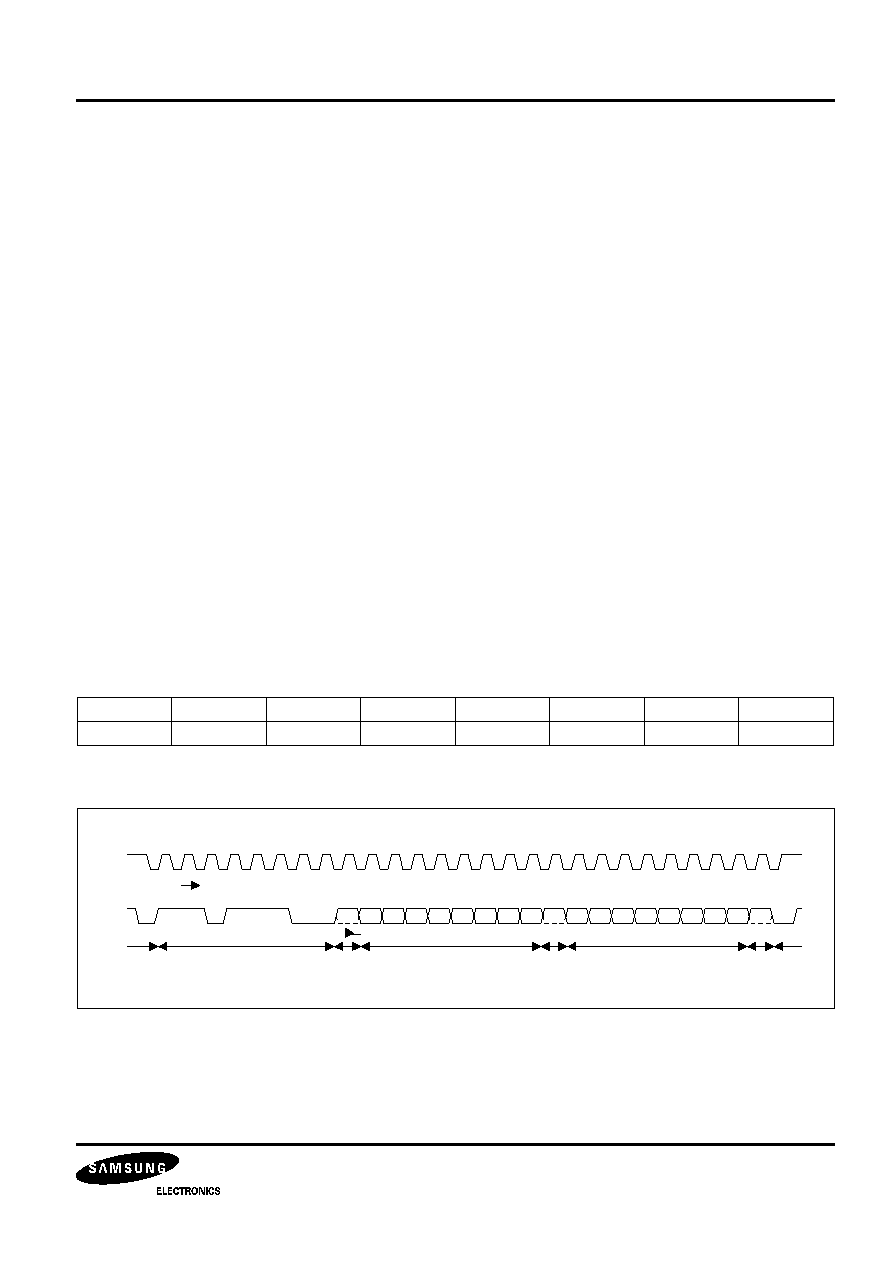
FUNCTIONAL DESCRIPTION
OSD INTENSITY INPUT (ACTIVE: HIGH)
This input pin is used to indicate the OSD color intensity.
Thus, 15 color selection is achievable by combining this intensity pin input with R/G/B OSD input.
If you do not want OSD intensity function, you have to connect this pin to ground. If this pin is in high state
(normally 5V), the level of OSD output will be attenuated to 50% of original OSD output.
The family of samsung OSD IC supports the OSD intensity output function.
OSD INPUTS
The S1D2518X01 includes all the circuitry necessary to mix OSD signals into the R/G/B video signal.
You need 4 pins for function. (R/G/B OSD, OSD blanking)
DATA TRANSFER
All bytes are sent MSB (Most Significant Bit) bit first and the write data transfer is closed by a stop.
The MCU can write data into the S1D2518X01 registers. To do that, after a start, the MCU must send:
∑
The I
2
C address slave byte with a low level for R/W bit (bit1)
∑
The byte of the internal register address where the MCU wants to write data (sub address)
∑
The data
∑
Stop
Serial Interface
The 2-wires serial interface is an I
2
C bus interface.
The slave address of the S1D2518X01 is DC (hexadecimal)
I
2
C Bus Write Operation: A complete data transfer
Bit8
Bit7
Bit6
Bit5
Bit4
Bit3
Bit2
Bit1
1
1
0
1
1
1
0
0 (W)
Stop
ACK
Data Byte
ACK
ACK
Register Address
Slave Address
Start
Generated by Slave
W
MSB
LSB
SCL
SDA
Transfer
S1D2518X01 I
2
C BUS CONTROLLED R/G/B VIDEO AMPLIFIER FOR MONITORS
18
Preliminary
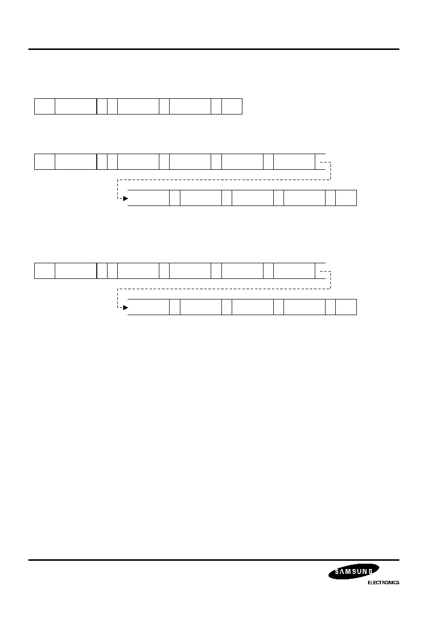
Data Transfer Format
∑
1Byte Data Transfer
∑
Multi Data Transfer
∑
Automatic Increment
The automatic increment feature of the sub address enables a quick slave receiver initialization within one
transmission, by the I
2
C bus controller
STA
Slave Adrs
W A
Sub Adrs
A
Data
A
STO
STA
Slave Adrs
W A
Sub Adrs
A
Data
A
Sub Adrs
A
Data
A
Data
A
Sub Adrs
A
Data
A
STO
STA
Slave Adrs
W A
Auto Adrs
(1XXX0000)
A
Data
(sub: 00H)
A
Data
(sub: 01H)
A
Data
(sub: 03H)
A
Data
(sub: 09H)
A
Data
(Sub: 0AH)
A
Data
(sub: 0BH)
A
STO
I
2
C BUS CONTROLLED R/G/B VIDEO AMPLIFIER FOR MONITORS S1D2518X01
19
Preliminary
SUB ADDRESS ALLOCATION MAP (SLAVE ADDRESS: DCH)
∑
SBLK: Soft blanking switch (1: on, 0: off)
∑
CPS: Clamping input polarity selection (1: pos., 0: neg.)
∑
NSS: No Signal Switch (1: on., 0: off.)
If this bit is set to `1', this bit blanks the video signal except OSD signal
∑
HT: Video & OSD half tone (1: on, 0: off)
∑
CS1/2: Extended cut-off brightness offset current control data bits (CS1 = 90uA/CS2 = 170uA)
∑
IS2/IS1: OSD intensity mode switch
Sub Address
(Hex)
Function
DAC Bits
Int. Value
(Hex)
D7
D6
D5
D4
D3
D2
D1
D0
00H
Contrast control
8 bits
80H
01H
SBLK
CS2
CS1
Brightness control (3-ch)
8 bits
00H
02H
SUB contrast control (R)
8 bits
80H
03H
SUB contrast control (G)
8 bits
80H
04H
SUB contrast control (B)
8 bits
80H
05H
OSD contrast control
-
-
-
-
4 bits
80H
06H
Cut-off brightness control
8 bits
80H
07H
Cut-off control (R)
8 bits
80H
08H
Cut-off control (G)
8 bits
80H
09H
Cut-off control (B)
8 bits
80H
0AH
DAC
8 bits
80H
0BH
T3
T2
T1
NSS
CPS
IS2
IS1
HT
-
E0H
IS2
IS1
Mode
0
0
R/G/B color intensity
0
1
G/B color intensity
1
0
R/B color intensity
1
1
R/G color intensity
<15 Color>
<8 Color>
R
G
B
R
G
B
INT

S1D2518X01 I
2
C BUS CONTROLLED R/G/B VIDEO AMPLIFIER FOR MONITORS
20
Preliminary
REGISTER DESCRIPTION
Contrast Adjustment (8 bits)
The contrast adjustment is made by controlling simultaneously the gain of three internal variable gain amplifiers
through the I
2
C bus interface.
The contrast adjustment allows you to cover a typical range of 38dB.
OSD Contrast Adjustment (4 bits)
The OSD contrast adjustment is made by controlling simultaneously the gain of three internal variable gain
amplifiers through the I
2
C bus interface.
The OSD contrast adjustment allows you to cover a typical range of 38dB.
Brightness Adjustment (5 bits)
The brightness adjustment controls to add the same black level (pedestal) to the 3-channel /R/G/B signals after
contrast amplifier by I
2
C bus.
Cut-Off Brightness Adjustments (8 bits)
The cut-off brightness adjustment is made by simultaneously controlling the external cut-off current.
SUB Contrast Adjustment (8 bits
◊
◊
◊
◊
3)
The SUB contrast adjustment allows to cover a typical range of 12dB.
Cut-Off Adjustments (8 bits
◊
◊
◊
◊
3)
These adjustments are used to adjust the white balance, and the gain of each channel is controlled by I
2
C bus.
Contrast Register (SUB ADRS: 00H) (Vin = 0.56Vpp, bright: 00H, sub: FFH)
Brightness Register (3-ch) (sub adrs: 01H) (cont: 80H, sub: 80H)
Hex
Bits
Contrast
(Vpp)
Gain
(dB)
Int. Value
(Hex)
B7
B6
B5
B4
B3
B2
B1
B0
00
0
0
0
0
0
0
0
0
0
-35.0
80
1
0
0
0
0
0
0
0
2.1
11.5
O
FF
1
1
1
1
1
1
1
1
4.2
17.5
Increment/bit
0.0164
Hex
Bits
Brightness
(V)
Int. Value
(Hex)
B4
B3
B2
B1
B0
00
0
0
0
0
0
0.6
O
1F
1
1
1
1
1
1.8
Increment/bit
0.038

I
2
C BUS CONTROLLED R/G/B VIDEO AMPLIFIER FOR MONITORS S1D2518X01
21
Preliminary
SUB Contrast Register (3-ch) (sub adrs: 02/03/04H) (Vin = 0.56Vpp, bright: 00H, cont: FFH)
OSD Contrast Register (sub adrs: 05H) (VOSD = TTL, bright: 00H, sub: FFH)
Cut-Off Brightness Register (3-ch) (sub adrs: 06H)
Cut-Off Register (3-ch) (sub adrs: 07/08/09H)
DAC Register (sub adrs: 0AH)
Hex
Bits
Sub Contrast
(Vpp)
Gain
(dB)
Int. Value
(Hex)
B7
B6
B5
B4
B3
B2
B1
B0
00
0
0
0
0
0
0
0
0
1.33
7.5
80
1
0
0
0
0
0
0
0
2.65
13.5
O
FF
1
1
1
1
1
1
1
1
4.2
17.5
Increment/bit
0.0123
Hex
Bits
OSD Contrast
(Vpp)
Gain
(dB)
Int. Value
(Hex)
B7
B6
B5
B4
B3
B2
B1
B0
00
0
0
0
0
-
-
-
-
0
-
80
1
0
0
0
-
-
-
-
2.4
-
O
FF
1
1
1
1
-
-
-
-
4.0
-
Increment/bit
0.25
Hex
Bits
Cut-Off Brightness
(uA)
Int. Value
(Hex)
B7
B6
B5
B4
B3
B2
B1
B0
00
0
0
0
0
0
0
0
0
0
80
1
0
0
0
0
0
0
0
100
O
FF
1
1
1
1
1
1
1
1
200
Increment/bit
0.781
Hex
Bits
Cut-Off EXT
(uA)
Int. Value
(Hex)
B7
B6
B5
B4
B3
B2
B1
B0
00
0
0
0
0
0
0
0
0
0
80
1
0
0
0
0
0
0
0
250
O
FF
1
1
1
1
1
1
1
1
500
Increment/bit
1.953
Hex
Bits
DAC OUT
(uA)
Int. Value
(Hex)
B7
B6
B5
B4
B3
B2
B1
B0
00
0
0
0
0
0
0
0
0
0
80
1
0
0
0
0
0
0
0
250
O
FF
1
1
1
1
1
1
1
1
500
Increment/bit
1.953

S1D2518X01 I
2
C BUS CONTROLLED R/G/B VIDEO AMPLIFIER FOR MONITORS
22
Preliminary
APPLICATION POINT
12V Power Routing
Because S1D2518X01 is a wideband AMP of above 150MHz, 12V power significantly affects the video
characteristics. The effects from the inductance and capacitance are different for each board, and , therefore,
some tuning is required to obtain the optimum performance. The output power, VCC2, must be separated from
VCC1 using a bead or a coil, which is parallel-connected to the damping resistor. In the case of using a coil , the
appropriate coil value is between 0.1uH to 100uH. Parallel-connected a variable resistor to the coil and control its
resistance to obtain the optimum video waveform.
(Bead use: Refer to Application Circuit )
(Moreover, bead can be replaced using a coil and variable resistor to obtain the optimum video waveform.)
VCC1 12V Power
Use a 104 capacitor and large capacitor for the power filter capacitor.
12V Output Stage Power VCC2
Do not use the power filter capacitor or use a capacitor smaller than 22pF, because it is an important factor of
video oscillation. The coil, resistor and by-pass capacitor for 27 pin B+ must be placed as close as possible to the
Vcc2 pin.
Output Stage GND2
Care must be taken during routing because it ,as an AMP output stage GND, is an important factor of video
oscillation. R/G/B clamp cap and R/G/B load resistor must be placed as close as possible to the GND2 pin. GND2
must be arranged so that it has the minimum GND loop.
R/G/B Clamp Capacitor
Use the 104 capacitor for normal R/G/B clamps.
During the clamp signal's input period, the clamp stage compares the video output's pedestal level and the level
adjusted by sub address 01. If an error is detected, current is charged/discharged to the clamp capacitor, so that
the video output pedestal level is set to the adjusted level.
The current charged/discharged to the clamp cap is about 750uA. The capacitor value is very important.
If the R/G/B clamp cap's charge current is different for each channel, the screen can first appear to be red or blue,
then later become normal when you turn the power on. In that case, it is best to change the clamp cap value to
adjust the charge/discharge time.
DC Coupling Capacitor
Select the video input DC coupling cap with sagging in mind.
Select from between 10uF and 0.1uF.
S1D2518X01 I
2
C BUS CONTROLLED R/G/B VIDEO AMPLIFIER FOR MONITORS
23
Preliminary
Clamp Pulse
The clamp pulse receives its input from the U-Processor and needs a minimum pulse width of 200ns. An active low
signal with a pulse width of 500 to 700ns is recommended. But you can change the clamp pulse polarity using CPS
bit.
If the clamp signal is high during mode change, gm2's clamp operation does not occur. A charge or discharge
occurs in the output clamp cap, caused by the transistor's leakage component. This results in a change in the
clamp cap's voltage, which can influence the brightness of the screen. Therefore, it is best to supply a low level
clamp signal or a pseudo clamp signal during a transient period like that of mode change.
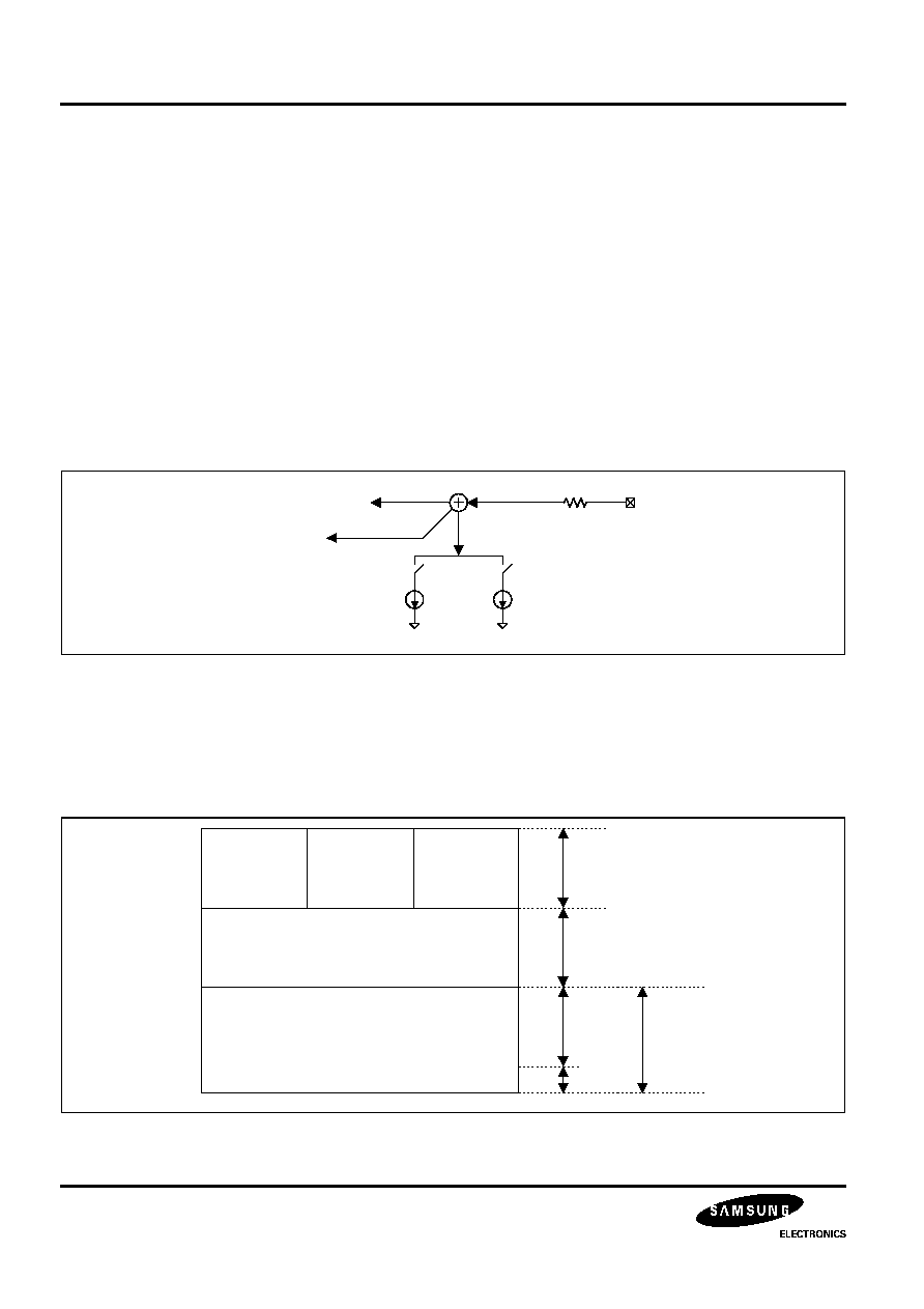
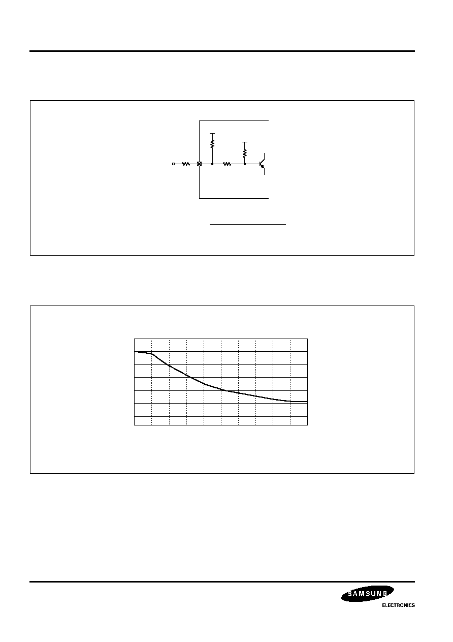
Cut-Off Control and Cut-off Brightness Control (RCT, GCT, and BCT pins Applications)
This feature, which is an external application for most other products, is built into the IC in S1D2518X. It controls
the CRT bias voltage of each R/G/B channel to adjust the raster white balance. Also set brightness can be
controlled through the same pins. If the set brightness control is not done at G1, the cut-off brightness control is
very useful. Three DACs are needed.
Figure 4. Internal Diagram
It is basically configured as a current mirror.
Cut-off range control through an external pin is decided by the current sinking amount at the RCT/GCT/BCT pins.
Total external cut-off current range
ICT
(Cut-off current)
IBRT
(Cut-off brightness current)
ICS
90uA
170uA
CS1
CS2
(offset current)
ICTX
Pin 17, 18, 19
RED
Cut-off
GREEN
Cut-off
(ICT)
BLUE
Cut-off
Cut-off Brightness
(IBRT)
Cut-off Offset Switch
(ICS)
CS1
CS2
500uA
200uA
170uA
90uA
260uA
I
2
C BUS CONTROLLED R/G/B VIDEO AMPLIFIER FOR MONITORS S1D2518X01
24
Preliminary
IBRT is the cut-off brightness current which simultaneously controls 3 channels. Its range is 0 ≠ 200uA.
ICS is an offset current which simultaneously controls 3 channels through the combination of 2-bit. Its range is 0,
90, 170, and 260uA.
ICT is a cut-off control which can control from 0 ≠ 500uA per channel.
ICT and ICS currents are used in white balance adjustment.
IBRT and ICS currents are used when controlling brightness in the set.
ICTX = ICT + ICS + IBRT
(0 ≠ 500uA) + (0 ≠ 260uA) + (0 ≠ 200uA)
(0 ≠ 960uA)
≠ R.G.B Cut-off control (Raster white balance control)
Maximum control current by cut-off register (8 bits): 500
µ
A
1-bit control current: 1.96
µ
A
When you use 75V ≠ 80V for cut-off stage Vcc,
CS2, CS1 bit status of S1D2518X should be selected by 0.
If these data selects 1, the offset current of the cut-off control will be increased to 260
µ
A. Therefore, these data
(CS2, CS1) need to be set to 0.
But if Vcc for the cut-off stage increases to something like 220V, you need to change the data to 1 by the set
status.
≠ Cut-off Brightness Control (Set brightness control)
This function is to adjust the brightness. It is composed of 8 bits.
Sub address is 06.
Maximum control current is 200
µ
A (0.78
µ
A/1bit).
By adjusting this sub address, you can handle the set brightness. This adjustment simultaneously moves
one point of the cut-off DC to R/G/B
Figure 5. Outside Application Circuit
80V
17
A
75K
75K
R1
From Driver
IC
B
To CDTS
Cathode
1N4148
Q2
Q1
2.2K
104
50V
1uF
100V
12V
ICTX
Q1 : Protection transistor for S1D2518X
Q2 : Clamping transistor
: This point voltage will keep 11.3V every time
A

S1D2518X01 I
2
C BUS CONTROLLED R/G/B VIDEO AMPLIFIER FOR MONITORS
25
Preliminary
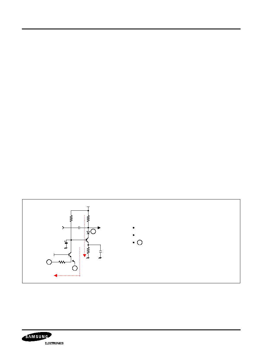
R/G/B cut-off control and cut-off brightness control are carried out through the same route. The amount of the
voltage drop is the product of the sinking current amount of S1D2518X's pin17 and the R1 value. Therefore, the B
point's voltage is 80V - (sinking current x R1) + 2Vbe. If the value of R1 is large, the Resolution quality is lessened,
but the voltage control range is increased. Since the routes of the cut-off control current and the cut-off brightness
control current are the same, the sinking current amount and R1 value should be adjusted for appropriate values to
the set's specifications.
≠ Cut-off and Set Brightness Control Method
You can use two methods for cut-off and set brightness control.
The RCT, GCT and BCT pins are composed of open collector type.
The pin configuration is like that.
The first method is using current DAC configuration.
In this method, sunk current amounts decide cut-off voltage. You used 75V, 75k
and 500uA sunk current in the
application circuit. Then the cut-off bias voltage is 75V - (75k
x 500uA) + 2Vbe = 39V.
If you reduce the resistor R1 value or sunk current, then the cut-off bias voltage level goes high. (39V
)
0.2k
S1D2518X
Rout
Generic
Driver
IC
75k R1
75k
2.2k
0.47uF
50V
47
1uF
100V
12V
RCT
75V
BAV21
I
2
C BUS CONTROLLED R/G/B VIDEO AMPLIFIER FOR MONITORS S1D2518X01
26
Preliminary
Refer to typical application circuit.
CS1/CS2: Cut-off control offset current for AC coupling.
CS1 bit = 1: Cut-off control current + 90uA current sunk
CS2 bit = 1: Cut-off control current + 170uA current sunk
CS1 bit = 1, CS2 bit = 1: Cut-off control current + 90uA + 170uA current sunk
If CS1 bit =1, CS2 bit =1, cut-off register = FF, and cut-off brightness register = FF, then 90uA + 170uA + 500uA +
200uA = 960uA current sunk by S1D2518X 17, 18, 19 pins (each channel).
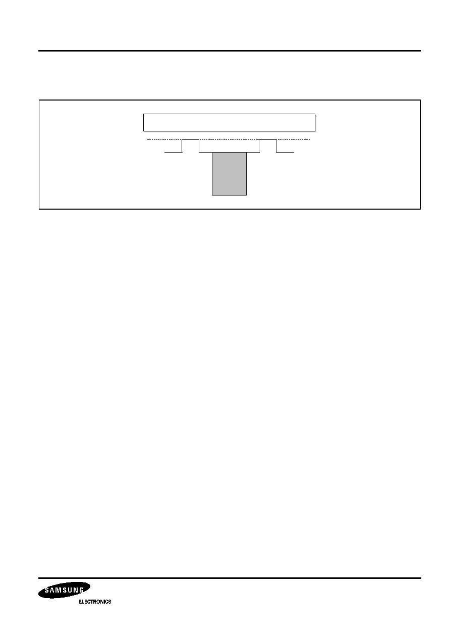
39V
Video Signal Waveform Measured by Cathode Part

S1D2518X01 I
2
C BUS CONTROLLED R/G/B VIDEO AMPLIFIER FOR MONITORS
27
Preliminary
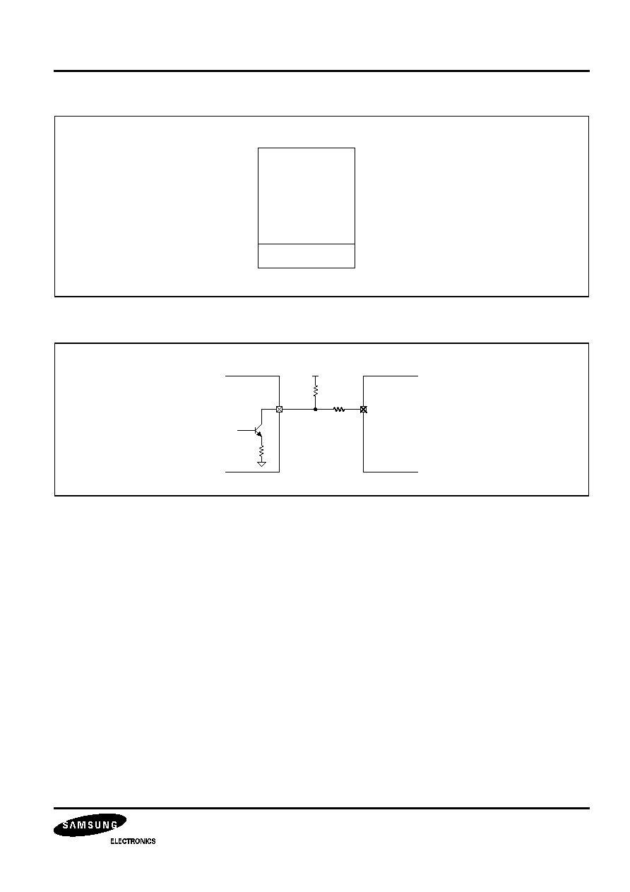
The second method is using generic cut-off control IC.
In second method, you must use pull-up resistor.
Case 1. 5V Pull-up
In above picture, RCT pins outputs 5V - (From 0 to 500uA ) x 10K = from 5V to 0.3V DC level.
So, all kinds of cut-off IC using 0 - 5V input range can be used.
∑
cut-off Register : 00H
5V
FFH
5V - 10K x 500uA = 0.3V
∑
cut-off Brightness Register : 00H
5V
FFH
5V - 10K x 200uA = 3V
When using 10k pull-up resistor, you can get the 5V output range.
But, the 5V range include cut-off bright range. So, if you set 1V bright range, you must consider 1.3 - 5V cut-off
range for white balance.
S1D2518X
Generic
Cut off IC
RCT
0.2k
5V
10k
100
S1D2518X
Rout
Generic
Driver
IC
75V
10uF
RCT
75V
5V
10k
0.1uF
1k
Generic
Cut off
IC
330k
0.1uF
0.1uF
I
2
C BUS CONTROLLED R/G/B VIDEO AMPLIFIER FOR MONITORS S1D2518X01
28
Preliminary
Case 2. 12V Pull-up
In above picture, cut-off IC input is 0.3V to 4.25V.
So, all kinds of cut-off IC using 0 - 5V input range can be used.
∑
Cut-off IC input voltage (cut-off brightness register : 00H)
4.25V : Cut-off register 00H
1.40V : Cut-off register FFH
∑
Cut-off IC input voltage (cut-off register : 00H)
4.25V : Cut-off Brightness register 00H
2.85V : Cut-off Brightness register FFH
ABL
The ABL detects the amount of current flowing into the CRT cathode to lower the brightness of the screen. The
S1D2518X uses the ABL pin's feedback voltage to control the contrast.
The lower the ABL input voltage, weaker the video signal.
When open, the ABL is floated to 12V and doesn't operated.
When S1D2518X's ABL function is not being used, the ABL pin is connected to a cap in a series to connect to the
GND.
Ripple extract capacitor must be used. It's value depends on the set characteristics, but normally it uses 1uF -
10uF/16V.
For white
balance conrol
0.3V
For bright control
1.3V
5V
S1D2518X
Generic
Cut off IC
RCT
0.2k
12V
18k
43k
S1D2518X01 I
2
C BUS CONTROLLED R/G/B VIDEO AMPLIFIER FOR MONITORS
29
Preliminary
The pin configuraion is like that.
The ABL curve characteristic is like below.
If there is only the oscillation in a full white patten with a large gain, you must increase the ripple extract capacitor's
value.
50k
12V
2.5V
5k
30k
ZI
V
ABLPIN
=
1/Z
I
+ 1/50k + 1/35k
V
I
/Z
I
+ 12/50k + 2.5/35k
VI
6.1V
5
4
3
2
1
5
3
4.5
2.5
2
1
0.5
4
0
Video Out [V]
- Video Input Level : 0.7Vpp
- Contrast and sub contrast register : FFH
V
ABLPIN
[V]

I
2
C BUS CONTROLLED R/G/B VIDEO AMPLIFIER FOR MONITORS S1D2518X01
30
Preliminary
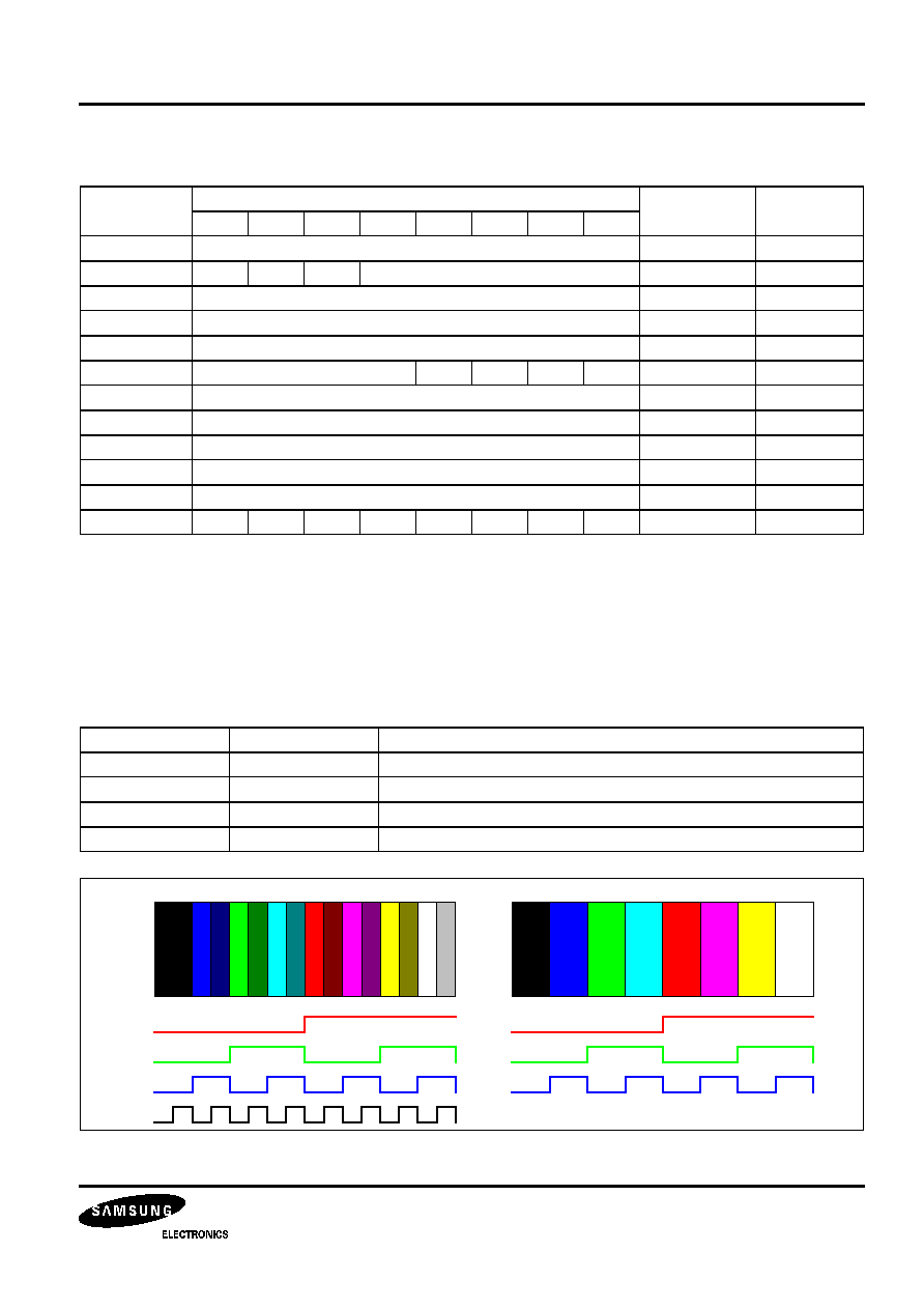
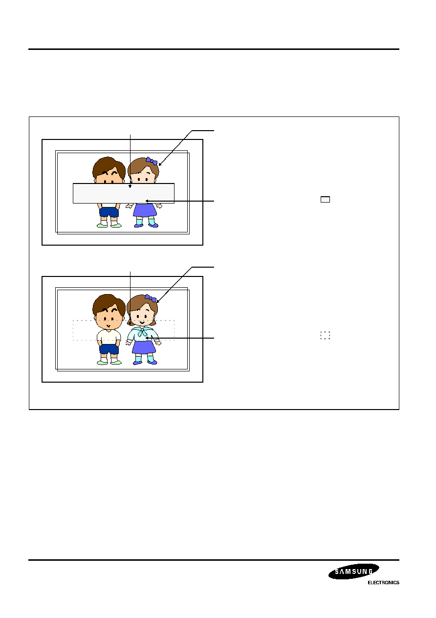
Video/OSD Half Tone
This feature allows you to handle the OSD character information in a special way that reduces stress on your eyes
even for a static screen, and significantly lessens the influence of the character information on the image signals.
These effects result in facilitating the relaying of information to you.
- Half tone: Loads half of the video and OSD signal gain to the OSD raster to emphasize the OSD characters and
the raster.
Video/OSD HALF Tone Timing Chart
R OSD In
G OSD In
B OSD In
Video In
OSD SW
HALF TONE
R Video Out
G Video Out
B Video Out
S1D2518X01 I
2
C BUS CONTROLLED R/G/B VIDEO AMPLIFIER FOR MONITORS
31
Preliminary
HT bit = 1, video & OSD half tone function is on.
Then you can see the video signal & OSD.
Monitor Set Display Screen
Monitor Set Display Screen
A
B C D
A
B C D
OSD Character (ABCD)
Video Signal (image)
Selected Mode OSD Back Raster ( )
(8 possible colors: Green, Blue, Black, Cyan
Normal Monitor Screen (video signal cut off by OSD raster)
OSD Character (ABCD)
Video Signal (image)
Selected Mode OSD Back Raster ( )
Moniter screen in video & OSD half-tone state (OSD signal is reduced by 1/2, and a video signal with its gain
reduced by 1/2 is shown in the OSD raster area.)
Red, Magenta, Yellow, White)

I
2
C BUS CONTROLLED R/G/B VIDEO AMPLIFIER FOR MONITORS S1D2518X01
32
Preliminary
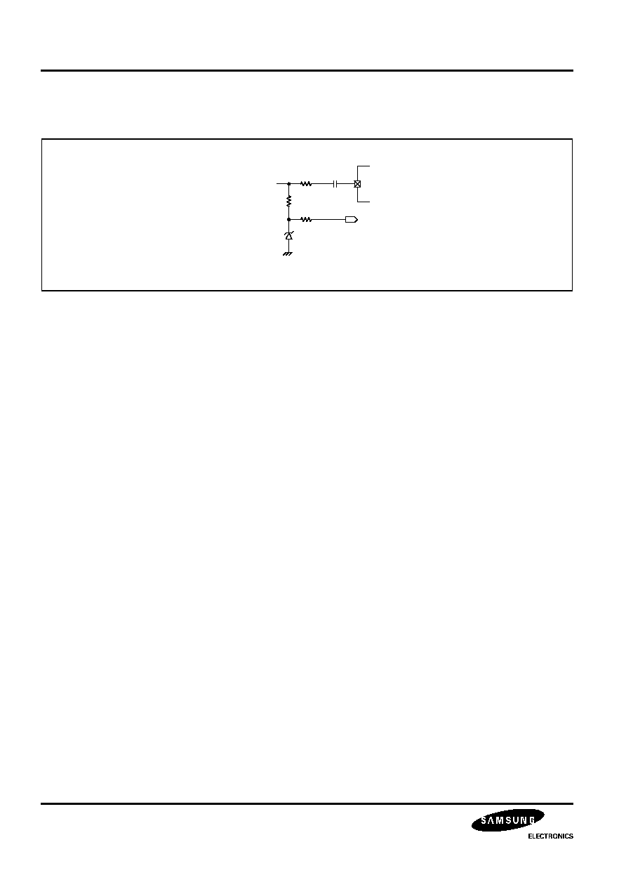
Horizontal Blank Pulse
The horizontal blank pulse receives its input from the monitor horizontal scan.
The typical horizontal blank pulse width is 3
µ
S. The pin configuration is like that.
You can use three types of horizontal blank pulse.
The first is the original positive horizontal blank pulse with integration circuit and differentiation circuit.
If you increase the width of horizontal blank pulse, you have to increase C1'S value.
The second is the positive TTL logic signal.
The threshold voltage of the horizontal blank pulse is the 0.7V.
5V
0.224k
10k
150
1N4148
1nF
100V
2K
10K
330P
50V
C1
4.7nF
100V
HFLB
HFLB
100P
2.4K
1N4148
5V
2N3904
560K
S1D2518X01 I
2
C BUS CONTROLLED R/G/B VIDEO AMPLIFIER FOR MONITORS
33
Preliminary
The third is the original positive horizontal blank pulse.
No Signal Switch Function (NSS)
If this bit is set to `1', this bit blank the video signal except OSD signal.
If input timing mode is sync out of range, you set the NSS bit to `1', then you can see OSD and clean raster.
HFLB
2.2k
8.2nF
10k
1.5k
6.2V
Zener Diode
to OSD

I
2
C BUS CONTROLLED R/G/B VIDEO AMPLIFIER FOR MONITORS S1D2518X01
34
Preliminary
POWER SCHEME
9.6V
(Spot Killer Voltage)
10.8V
11.4V
12V
12.6V
13.2V
15V
(Max. Supply Voltage)
Recommended
operation voltage
Operation voltage
(Video and OSD output signal
gains are changed according to
V
CC
variations)
V
CC
3V
(POR. Voltage)
4.25V
4.75V
5V
5.25V
5.75V
7V
(Max. Supply Voltage)
V
DD
Recommended
operation voltage
Operation voltage

S1D2518X01 I
2
C BUS CONTROLLED R/G/B VIDEO AMPLIFIER FOR MONITORS
35
Preliminary
APPLICATION BOARD CIRCUIT
S1D2518X01
1
2
3
4
5
6
7
8
10
9
11
12
13
14
15
30
29
28
27
26
25
24
23
21
22
20
19
18
17
16
ROSD
GOSD
BOSD
VI/OSD_SW
RIN
VCC1
GND1
GIN
BIN
VCC3
GND3
ABL
SCL
SDA
VDD
INT
RCLP
ROUT
GCLP
GOUT
VCC2
GND2
BOUT
BLK
BCLP
CLP
RCT
GCT
BCT
DAC OUT
ROSD IN
GOSD IN
BOSD IN
VI/OSD SW
IN
RED IN
10u
+
+
0.075K
0.033K
10u
0.1u
GREEN IN
10u
+
+
0.075K
0.033K
10u
0.1u +
BLUE IN
0.075K
4.7u
ABL IN
SCL
SDA
0.1K
0.1K
+
100u
VDD = 5V
2K
2K
0.033K
0.033K
0.033K
0.033K
0.033K
0.1K
0.1K
0.1K
0.1K
1u
2.2K
1u
12V
75V
75K
75K
B Drive Out
Cathode B
1u
2.2K
1u
12V
75V
75K
75K
Cathode G
G Drive Out
1u
2.2K
1u
12V
75V
75K
75K
R Drive Out
Cathode R
CLP IN
0.1K
BLK IN
0.39K
BOUT
GOUT
0.1u
0.1u
0.1u
ROUT
INT
+
0.1u
470u
VCC = 12V
BAV21
BAV21
BAV21
10u
0.39K
0.39K
Bead
KSP42
KSP92
KSP42
KSP92
KSP42
KSP92
0.1K
104
5V
Bead

I
2
C BUS CONTROLLED R/G/B VIDEO AMPLIFIER FOR MONITORS S1D2518X01
36
Preliminary
TYPICAL APPLICATION CIRCUIT
4.
7u
ROSD
GOSD
BOSD
VI/OSD_SW
RIN
VCC1
GND1
GIN
BIN
VCC3
GND3
ABL
SCL
SDA
VDD
INT
RCLP
ROU
T
GCLP
GOUT
VCC2
GND2
BOUT
BLK
BCLP
CLP
RCT
GCT
BCT
DAC OUT
ROSD IN
GOSD IN
BOSD IN
VI/OSD SW IN
RED IN
10u
0.075K
10u
0.1u
GREEN IN
0.075K
0.033K
BLUE IN
4.7u
ABL IN
SCL
SDA
0.1K
VDD = 5V
2K
0.033K
0.033K
0.1K
1u
1u
12V
75V
75K
Cathode B
1u
2.2K
1u
12V
75V
75K
Cathode G
1u
2.2K
1u
12V
75V
75K
R Drive Out
Cathode R
CLP IN
0.1K
BLK IN
BIN
GIN
0.1u
0.1u
RIN
INT
0.1u
470u
VCC = 12V
BAV21
BAV21
BAV21
0.39K
KSP42
KSP92
KSP42
KSP92
KSP42
KSP92
VEE
1
2
3
4
5
6
7
8
9
10
11
12
13
14
15
30
29
28
27
26
25
24
23
22
21
20
19
18
17
16
0.033K
0.033K
10u
0.1u
10u
10u
0.033K
0.075K
0.1K
2K
0.1u
0.39K
10
10
10
0.39K
0.1K
0.1K
0.1K
100uF
0.1uF
VCC = 12V
VCC
ROU
T
GOUT
BOUT
0.1uF
75V
100uF
27
27
27
0.1uF
0.1uF
0.1uF
S1D2518X01
75K
75K
75K
0.1K
18p
0.33uH
49
2.2k
100u
1
0
4
5V
Bead

S1D2518X01 I
2
C BUS CONTROLLED R/G/B VIDEO AMPLIFIER FOR MONITORS
37
Preliminary
PACKAGE DIMENSION
NOTE: Dimensions are in millimeters.
27.88 MAX
27.48
+ 0.20
(1.30)
30-SDIP-400
8.94
+
0
.20
#30
#1
0.56
+ 0.10
1.12
+ 0.10
3.81
+
0.20
5.21 MAX
1.778
0.51 MIN
3.30
+
0.30
#16
#15
0-15
0.25
+ 0.10- 0.05
10.16