RF AMP & SERVO SIGNAL PROCESSOR
S1L9223B01
1
INTORDUCTION
The S1L9223B01 is a 1-chip BICMOS integrated circuit to perform the
function of RF amp and servo signal processor for compact disc
player applications.
It consist of blocks for RF signal processing, focus, tracking,
sled and spindle servo. Also this IC has adjustment free function
and embedded OP-AMP for audio post filter.
FEATURES
∑
RF amplifier & RF equalizer
∑
Focus error amplifier & servo control
∑
Tracking error amplifier & servo control
∑
Mirror & defect detector circuit
∑
Focus OK detector circuit
∑
APC (Auto Laser Power Control) circuit for constant laser power
∑
FE bias & focus servo offset adjustment free
∑
EF balance & tracking error gain adjustment free
∑
Embedded audio post filter
∑
The circuit for Interruption countermeasure
∑
Double speed play available
∑
Operating voltage range: S1L9223B01: 5V
ORDERING INFORMATION
RELATED PRODUCT
∑
S5L9286F01 Data Processor
∑
S5L9284D Data Processor
∑
KA9258D/KA9259D Motor Driver
Device
Package
Temperature Range
S1L9223B01-Q0R0
80-QFP-1420C
-
20 to +70
∞
C
80
-
QFP
-
1420C

S1L9223B01
RF AMP & SERVO SIGNAL PROCESSOR
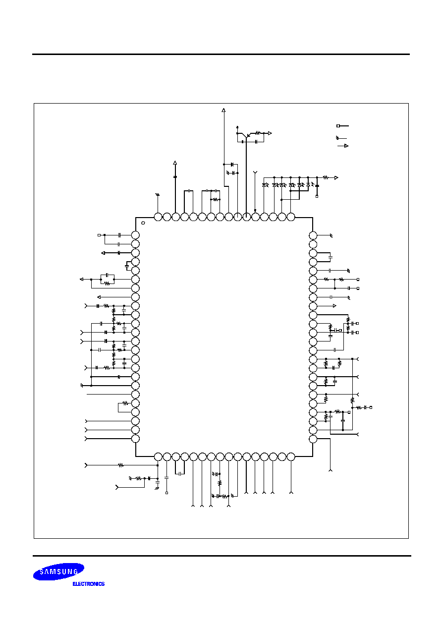
2
BLOCK DIAGRAM
73
74
65
66
63
67
68
79
69
70
71
78
76
75
32
33
77
2
4
RF Amp
59
Focus Error Amp
FE-BIAS Adjustment
Tracking Error Amp
E/F Balance & Gain
Control
APC Amp
LDON
Center Voltage Amp.
RF Level AGC
Equalizer
EFM
Comparator
Defect Detection
Circuit
54
22
30
29
31
38
37
36
35
51
52
58
26
28
27
MICOM Data
Interface Logic
60
47
48
57
49
50
53
55
62
61
43
44
42
46
45
23
24
25
6
39
1
40
5
15
16
13
14
19
17
12
11
9
10
Focus Phase
Compensation
& Offset cancel circuit
Tracking Phase
Compensation Block
& Jump Pulse GEN.
Sled Servo Amplifier
& Sled Kick GEN.
Spindle Servo LPF
( Double Speed )
Mirror Detection
Circuit
FOK Detection
Circuit
MICOM TO SERVO CONTROL
AUTO SEQUENCER
ADJUSTMENT-FREE CONTROL
Built-in Post Filter Amp ( L&R )
FS1~
FS4
TM1~
TM6
BAL1~
BAL5
PS1~
PS4
GA1~
GA5
RF-
RFO
PD1
PD2
F
E
EI
PD
LD
VR
EQO
IRF
ASY
EFM
RFI
DCB
DCC1
GC
1
O
GC
1
I
CH1
O
CH1I
MU
T
E
I
RRC
CH2
O
CH2I
GC
2
I
GC
2
O
FDFCT
FE-
FEO
TDFCT
TE-
TEO
TE2
LPFT
SLO
SL-
SL+
SPDLO
SPDL-
SMDP
SMON
SMEF
FSET
MIRROR
MCP
FOK
TG2
TGU
FE
1
TE
1
ML
T
TZ
C
FE
2
FL
B
FG
D
FS
3
3
&
WD
C
H
TRCNT
LO
CK
IS
T
A
T
R
ESET
MD
A
T
A
MC
K
AT
S
C
FRS
H
DCC2
FEBIAS
EQC

RF AMP & SERVO SIGNAL PROCESSOR
S1L9223B01
3
PIN CONFIGURATION
1
2
3
4
5
6
7
8
9
10 11 12 13 14 15 16 17 18 19 20 21 22 23 24
25
26
27
28
29
30
31
32
33
34
35
36
37
38
39
40
64 63 62 61 60 59 58 57 56 55 54 53 52 51 50 49 48 47 46 45 44 43 42 41
80
79
78
77
76
75
74
73
72
71
70
69
68
67
66
65
S1L9223B01
MC
P
DCB
FR
S
H
DCC2
DCC1
F
SET
VDDA
VCCP
GC2I
GC2O
CH2
I
CH2
O
CH1
O
CH1
I
GC1O
GC1I
RRC
VS
SP
MU
T
E
I
I
SET
VRE
G
WDCK
SM
DP
SM
O
N
SMEF
FLB
FS3
FGD
LOCK
TRCNT
ISTAT
ASY
EFM
VSSA
MCK
MDATA
MLT
RESET
MIRROR
FOK
DVEE
FEBI
AS
TG
2
TG
U
FD
F
C
T
FE
1
FE
2
TD
F
C
T
DVDD
LP
F
T
TE
1
TE
2
TZ
C
AT
S
C
TE
O
TE
-
FE
O
FE
-
SPDL
O
SPDL
-
SL
-
SL
O
SL
+
SST
O
P
GND
EI
EQC
RFI
EQO
IRF
RFO
RF-
VCC
VR
LD
PD
E
F
PD2
PD1

S1L9223B01
RF AMP & SERVO SIGNAL PROCESSOR
4
PIN DESCRIPTION
Pin No.
Symbol
Description
1
MCP
Capacitor connection pin for mirror hold
2
DCB
Capacitor connection pin for defect Bottom hold
3
FRSH
Capacitor connection pin for time constant to generate focus search waveform
4
DCC2
The input pin through capacitor of defect bottom hold output
5
DCC1
The output pin of defect bottom hold
6
FSET
The peak frequency setting pin for focus, tracking servo and cut off frequency of CLV
LPF
7
VDDA
Analog VCC for servo part
8
VCCP
VCC for post filter
9
GC2I
Amplifier negative input pin for gain and low pass filtering of DAC output CH2
10
GC2O
Amplifier output pin for gain and low pass filtering of DAC output CH2
11
CH2I
The input pin for post filter channel2
12
CH2O
The output pin for post filter channel2
13
CH1O
The output pin for post filter channel1
14
CH1I
The input pin for post filter channel1
15
GC1O
Amplifier output pin for gain and low pass filtering of DAC output CH1
16
GC1I
Amplifier negative input pin for gain and low pass filtering of DAC output CH1
17
RRC
The pin for noise reduction of post filter bias
18
VSSP
VSS for post filter
19
MUTEI
The input pin for post filter muting control
20
ISET
The input pin for current setting of focus search, track jump and sled kick voltage
21
VREG
The output pin of regulator
22
WDCK
The clock input pin for auto sequence
23
SMDP
The input pin of CLV control output pin SMDP of DSP
24
SMON
The input pin for spindle servo ON through SMON of DSP
25
SMEF
The input pin of provide for an external LPF time constant
26
FLB
Capacitor connection pin to perform rising low bandwidth of focus loop
27
FS3
The pin for high frequency gain change of focus loop with internal FS3 switch
28
FGD
Reducing high frequency gain with capacitor between FS3 pin
29
LOCK
Sled runaway prevention pin
30
TRCNT
Track count output pin
31
ISTAT
Internal status output pin

RF AMP & SERVO SIGNAL PROCESSOR
S1L9223B01
5
PIN DESCRIPTION
(Continued)
Pin No.
Symbol
Description
32
ASY
The input pin for asymmetry control
33
EFM
EFM comparator output pin
34
VSSA
Analog VSS for servo part
35
MCK
MICOM clock input pin
36
MDATA
MICOM data input pin
37
MLT
MICOM data latch input pin
38
RESET
Reset input pin
39
MIRROR
The mirror output for test
40
FOK
The output pin of focus OK comparator
41
SSTOP
The pin for detection whether pick_up position is innermost or not
42
SL+
The noninverting input pin of sled servo amplifier
43
SLO
The output pin of sled servo amplifier
44
SL-
The inverting input pin of sled servo amplifier
45
SPDL-
The noninverting input pin of spindle servo amplifier
46
SPDLO
The output pin of spindle servo amplifier
47
FE-
The inverting input pin of focus servo amplifier
48
FEO
The output pin of focus servo amplifier
49
TE-
The inverting input pin of tracking servo amplifier
50
TEO
The output pin of tracking servo amplifier
51
ATSC
The input pin for Anti-shock detection
52
TZC
The comaparator input pin for tracking zero crossing detection
53
TE2
Tracking servo input pin
54
TE1
Tracking error amplifier output pin
55
LPFT
The input pin of tracking error low pass filtering signal
56
DVDD
The power supply pin for logic circuit
57
TDFCT
The capacitor connection pin for tracking defect compensation
58
FE2
Focus servo input pin
59
FE1
Focus error amplifier output pin
60
FDFCT
The capacitor connection pin for focus defect compensation
61
TGU
The capacitor connection pin for high frequency tracking gain switch
62
TG2
The pin for high frequency gain change of tracking servo loop with internal TG2 switch

S1L9223B01
RF AMP & SERVO SIGNAL PROCESSOR
6
PIN DESCRIPTION
(Continued)
Pin No.
Symbol
Description
63
FEBIAS
Focus error bias voltage control pin
64
DVEE
The DVEE pin for logic circuit
65
PD1
The negative input pin of RF I/V amplifier1(A+C signal)
66
PD2
The negative input pin of RF I/V amplifier2(B+D signal)
67
F
The negative input pin of F I/V amplifier (F signal)
68
E
The negative input pin of E I/V amplifier (E signal)
69
PD
The input pin for APC
70
LD
The output pin for APC
71
VR
The output pin of (AVEE+AVCC)/2 voltage
72
VCC
VCC for RF part
73
RF-
RF summing amplifier inverting input pin
74
RFO
RF summing amplifier output pin
75
IRF
The input pin for AGC
76
EQO
The output pin for AGC
77
RFI
The input pin for EFM comparison
78
EQC
The capacitor connection pin for AGC
79
EI
Feedback input pin of E I/V amplifier for EF Balance control
80
GND
GND for RF part
RF AMP & SERVO SIGNAL PROCESSOR
S1L9223B01
7
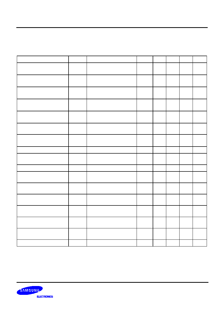
ABSOLUTE MAXIMUM RATINGS
ELECTRICAL CHARACTERISTICS
(Ta=25
∞
C, V
DD
= D
VDD
= V
CC
= +5V, V
SS
= D
VSS
= GND = V
SSP
= 0V)
Characteristic
Symbol
Value
Unit
Supply Voltage
V
MAX
6
V
Power Dissipation
P
D
200
mW
Operating Temperature
T
OPR
-
20 to + 70
o
C
Storage temperature
T
STG
-
55 to + 150
o
C
Characteristic
Symbol
Test Conditions
Output
Min.
Typ.
Max.
Unit
Supply Current High
ICCHI
V
CC
= 6V, No load
-
20
40
60
mA
Supply Current Typ
ICCTY
V
CC
= 5V, No Load
-
12
30
48
mA
Supply Current Low
ICCLO
V
CC
= 3.4V, No Load
-
10
25
40
mA
RF Amp Offset Voltage
Vrfo
Input open
pin 74
-
80
0
+80
mV
RF Amp Voltage Gain
Grf
SG3 f = 10kHz,
40mVp-p, sine
pin 74
25.1
28.1
31.1
dB
RF THD
Grfmd
SG3 f =1kHz, 40mVp-p,sine
pin 74
-
-
5
%
RF Amp Max. Output Voltage Vrfpp1
SG3 DC 2.7V
pin 74
3.8
-
-
V
RF Amp Min. Output Voltage Vrfpp2
SG3 DC 2.3V
pin 74
-
-
1.2
V
Focus Error Amp Offset
Voltage
Vfeo1
input open
pin 59
-
450
-
250
-
50
mV
Focus Error Amp Auto Offset
Voltage
Vfeo2
WDCH=88.2kHz Pulse,
$841
pin 59
-
35
0
35
mV
Focus Error Amp PD1
Voltage Gain
Gfe1
SG3 f=10kHz, 32mVp-p,
sine
pin 59
27
30
33
dB
Focus Error Amp PD2
Voltage Gain
Gfe2
SG3 f = 10kHz, 32mVp-p,
sine
pin 59
27
30
33
dB
Focus Error Amp Voltage
Difference
Gfe
Gfe1-
Gfe1
pin 59
-
3
0
+3
dB
Focus Error Amp Max.
Output Voltage
Gfepp1
SG3 DC 2.7V
pin 59
4.4
-
-
V
Focus Error Amp Min. Output
Voltage
Gfepp2
SG3 DC2.3V
pin 59
-
-
0.6
V

S1L9223B01
RF AMP & SERVO SIGNAL PROCESSOR
8
ELECTRICAL CHARACTERISTICS (Continued)
(Ta=25
∞
C, V
DD
= D
VDD
= V
CC
= +5V, V
SS
= D
VSS
= GND = V
SSP
= 0V)
Characteristic
Symbol
Test Conditions
Output
Min.
Typ.
Max.
Unit
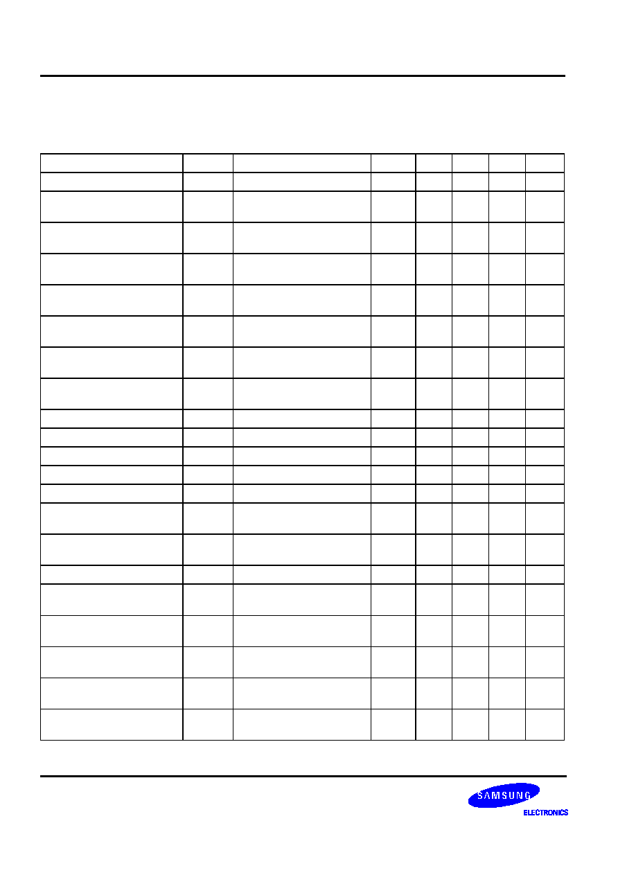
AGC Max Gain
Gagc
SG4 f = 500kHz, 20mVp-p,
sine
pin 76
16
19
22
dB
AGC EQ Gain
Geq
Gain Difference of Gagc at
f =1.5MHz
pin 76
0
1
2
dB
AGC Gain2
Gagc2
SG4 f = 500kHz, 0.5Vp-p,
sine
pin 76
3.5
6
9
dB
AGC Compress Ratio
Cagc
Gain Difference of Gagc2 at
0.1Vp-p
pin 76
0
2.5
5
dB
AGC Frequency
Fagc
Gain Difference
SG4 f=1.5MHz,0.1Vp-p,sine
and f=500kHz,0.1Vp-p,sine
pin 76
-
1.5
0
2.5
dB
Tracking Error Offset Voltage Vteo
$800, $820, input open
pin 54
-
50
0
+50
mV
Tracking Error Amp Voltage
Gain F
Gtef
$800, $820
SG3 0.3Vp-p, 10kHz, sine
pin 54
2.1
5.1
8.1
dB
Tracking Error Amp Voltage
Gain E
Gtee
SG3 0.3Vp-p, 40kHz, sine
pin 54
-
0.75
2.25
5.25
dB
Tracking Error Amp
Voltage Gain Difference
Gte
Gtef-Gtee
pin 54
-
0.25
2.75
5.75
dB
Tracking Error Amp
Maximum Output Voltage H
Vtepp1
DG3 DC 4.5V
pin 54
3.5
-
-
V
Tracking Error Amp
Minimum Output Voltage L
Vtepp2
SG3 DC 0.5V
pin 54
-
-
1.5
V
Tracking Error Amp Gain up
F
Tguf
$830 SG3 0.3Vp-p, 10kHz,
sine
pin 54
8.0
11.0
14.0
dB
Tracking Error Amp Gain up
E
Tgue
$830 SG3 0.3Vp-p, 10kHz,
sine
pin 54
5.3
8.3
11.3
dB
Tracking Gain Normal
Fgfn
SG3 0.3Vp-p, 10kHz, sine,
$820
pin 54
2.1
5.1
8.1
dB
Tracking F Gain 1
Fgf1
SG3 0.3Vp-p, 10kHz, sine,
$821
pin 54
0.1
3.1
6.1
dB
Tracking F Gain 2
Fgf2
SG3 0.3Vp-p,10kHz, sine,
$822
pin 54
-
1.7
1.3
4.3
dB
Tracking F Gain 3
Fgf3
SG3 0.3Vp-p, 10kHz, sine,
$824
pin 54
-
5.0
-
2.0
1.0
dB
Tracking F Gain 4
Fgf4
SG3 0.3Vp-p, 10kHz, sine,
$824
pin 54
-
9.2
-
6.2
-
3.2
dB
RF AMP & SERVO SIGNAL PROCESSOR
S1L9223B01
9
ELECTRICAL CHARACTERISTICS (Continued)
(Ta=25
∞
C, V
DD
= D
VDD
= V
CC
= +5V, V
SS
= D
VSS
= GND = V
SSP
= 0V)
Characteristic
Symbol
Test Conditions
Output
Min.
Typ.
Max.
Unit
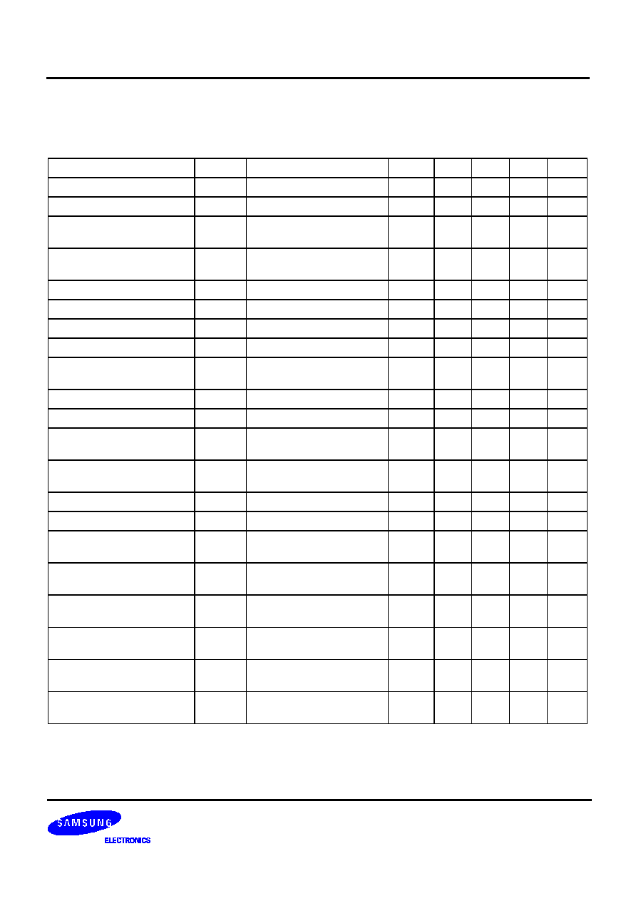
Tracking E Balance Normal
Tben
SG3 0.3Vp-p, 10kHz, sine,
$800
pin 54
-
0.27
2.27
5.27
dB
Tracking E Balance 1
Tbe1
SG3 0.3Vp-p, 10kHz, sine,
$801
pin 54
-
0.51
2.51
5.51
dB
Tracking E Balance 2
Tbe2
SG3 0.3Vp-p, 10kHz, sine,
$802
pin 54
-
0.74
2.74
5.74
dB
Tracking E Balance 3
Tbe3
SG3 0.3Vp-p, 10kHz, sine,
$804
pin 54
0.17
3.17
6.17
dB
Tracking E Balance 4
Tbe4
SG3 0.3Vp-p, 10kHz, sine,
$808
pin 54
1.03
4.03
7.03
dB
Tracking E Balance 5
Tbe5
SG3 0.3Vp-p, 10kHz, sine,
$810
pin 54
2.63
5.63
8.63
dB
FGFN-FGF1
FG1
-
-
0
1.5
3
dB
FGFN-FGF2
FG2
-
-
0.5
2.0
3.5
dB
FGFN-FGF3
FG3
-
-
2.0
3.2
4.5
dB
FGFN-FGF4
FG4
-
-
3.0
4.25
5.5
dB
TBE5
-
TBE4
TB1
-
-
0.6
1.6
2.6
dB
TBE4
-
TBE3
TB2
-
-
-
0.14
0.86
1.86
dB
TBE3
-
TBE2
TB3
-
-
-
0.57
0.43
1.43
dB
TBE2
-
TBE1
TB4
-
-
-
0.77
0.23
1.23
dB
APC PSUB Voltage 1
Vapc1
LDON, $853, PN=open,
SG4 GND+85mV
pin 70
-
-
1.2
V
APC PSUB Voltage 2
Vapc2
LDON, $853, PN=open,
SG4 GND+185mV
pin 70
3.8
-
-
V
APC NSUB Voltage 1
Vapc3
LDON, $857, PN=2.5V,
SG4 GND+95mV
pin 70
3.8
-
-
V
APC NSUB Voltage 2
Vapc4
LDON, $857, PN=2.5V,
SG4 GND+165mV
pin 70
-
-
1.2
V
APC LD Off Voltage 1
Vapc5
LDOFF, $85C, PN=open,
SG4 2.5V
pin 70
4.0
-
-
V
APC LD Off Voltage 2
Vapc6
LDOFF, $858, PN=2.5V.
SG4 2.5V
pin 70
-
-
1.0
V
APC Maximum Output
Current H
Vapc7
LDON, $854, PN=open,
SG4 GND + 185mV
pin 70
2.5
-
-
V
S1L9223B01
RF AMP & SERVO SIGNAL PROCESSOR
10
ELECTRICAL CHARACTERISTICS (Continued)
(Ta=25
∞
C, V
DD
= D
VDD
= V
CC
= +5V, V
SS
= D
VSS
= GND = V
SSP
= 0V)
Characteristic
Symbol
Test Conditions
Output
Min.
Typ.
Max.
Unit
APC Minimum Output
Current L
Vapc8
LDON, $854, SG4 GND +
85mV
pin 70
-
-
2.5
V
Mirror Maximum Output
Voltage H
Vmirh
SG4 2.1V+0.8Vp-p,
1kHz,sine
pin 39
4.3
-
-
V
Mirror Minimum Output
Voltage L
Vmirl
SG4 2.1V+0.8Vp-p,
1kHz,sine
pin 39
-
-
0.7
V
Mirror Minimum Operating
Frequency
Fmirh
SG4 2.1V + 0.8Vp-p,
900Hz,sine
pin 39
-
550
900
Hz
Mirror Maximum Operating
Frequency
Fmirb
SG4 2.1V+0.8Vp-p,
30kHz,sine
pin 39
30
75
-
KHz
Mirror AM Frequency
Characteristic
Fmir
SG4 2.1V+0.8Vp-p 600Hz,
fc=500kHz 55% modulation
pin 39
-
400
600
Hz
Mirror Minimum Input
Voltage
Vmir
SG4 2.1V + 0.2Vp-p,
10kHz,sine
pin 39
-
0.1
0.2
V
Mirror Maximum Input
Voltage
Vmih
SG4 2.1V+1.8Vp-p,
10kHz,sine
pin 39
1.8
-
-
V
FOK Threshold Voltage
Vfokt
SG4 2.25V~2.0V,DCsweep,
10mV step
pin 40
-
420
-
360
-
300
mV
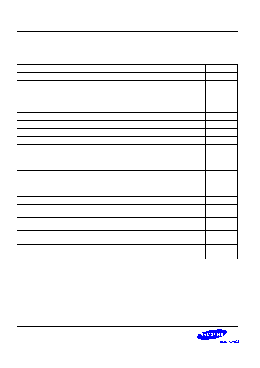
FOK Output Voltage H
Vfokh
SG4 DC 1.5V
pin 40
4.3
-
-
V
FOK Output Voltage L
Vfokl
SG4 DC 2.5V
pin 40
-
-
0.7
V
Defect Output Voltage H
Vdfcth
$863,SG3 2.520V+0.04Vp-p
f = 1kHz,sine
pin 41
4.3
-
-
V
Output Voltage L
Vdfcth
$863,SG3 2.520V+0.04Vp-p
f = 1kHz,sine
pin 41
-
-
0.7
V
Focus Loop Mute
Fmute
SG2 2.5V+0.1Vp-p
1kHz,sine
pin 48
-
100
0
100
mV
Tracking Loop Mute
Tmute
SG2 2.5V+0.1Vp-p
1kHz,sine
pin 50
-
100
0
100
mV
Interruption
Imute
SG2 2.5V+0.1Vp-p
1kHz,sine
pin 50
-
100
0
120
mV
Defect Bottom Voltage
Fdfct1
SG3 2.520 V+0.04Vp-p,
1kHz,sine
pin 41
-
670
1000
Hz
Defect Max Freq. Voltage
Fdfct2
SG3 2.520V+0.04Vp-p,
2kHz,sine
pin 41
2.0
4.7
-
KHz
RF AMP & SERVO SIGNAL PROCESSOR
S1L9223B01
11
ELECTRICAL CHARACTERISTICS (Continued)
(Ta=25
∞
C, V
DD
= D
VDD
= V
CC
= +5V, V
SS
= D
VSS
= GND = V
SSP
= 0V)
Characteristic
Symbol
Test Conditions
Output
Min.
Typ.
Max.
Unit
Defect Minimum Input
Voltage
Vdfct1
SG 3 2.510V+0.020Vp-p,
1kHz,sine
pin 41
-
0.3
0.5
V
Defect Maximum Input
Voltage
Vdfct2
SG32.535V+0.070Vp-p,
1kHz,sine
pin 41
1.8
-
-
V
EFM Duty Voltage 1
Defm1
SG4 2.5V+0.75Vp-p,
750kHz,sine
pin 32
-
50
0
50
mV
EFM Duty Voltage 2
Defm2
SG42.75V+0.75Vp-p,
750kHz,sine
pin 32
0
50
100
mV
EFM Minimum input Voltage
Vefm1
SG4 2.5V+0.12Vp-p,
750kHz,sine
pin 33
-
-
0.12
V
EFM Maximum input Voltage Vefm2
SG4 2.5V+1.8Vp-p
750kHz,sine
pin 33
1.8
-
-
V
EFM Maximum Operating
Frequency
Fefm
SG4 2.5V+0.75Vp-p
4MHz
pin 33
4
-
-
MHz
FZC Threshold Voltage
Vfzc
DC 2.5V+38mV,100mV
pin 31
35
69
100
mV
ATSC Threshold Voltage 1
Vatsc1
$10,SG2 DC 2.5V-6mV
-
45mV
pin 31
-
67
-
32
-
7
mV
ATSC Threshold Voltage 2
Vatsc2
SG2 DC 2.5V+6mV,+45mV
pin 33
7
32
67
mV
TZC Threshold Voltage
Vtzc
$20,SG2 DC 2.5V-20mV
+20mV
pin 31
-
30
0
30
mV
SSTOP Threshold Voltage
Vsstop
$30,SG2 DC 2.5V-71mV
-
30mV
pin 31
-
100
-
50
-
30
mV
Tracking gain window
voltage
VtGW
$840+$830 SG2 2.5V 2.9V
5mV DC
pin 30
200
250
300
mV
Tracking gain window range
VTGW2
$848+$830 SG2 2.5V 5mV
DC sweep
pin 30
100
150
200
mV
Tracking balance window
voltage
VTBW
$844+$810 SG2 2.555V ~
2.475V 5mV DC sweep
pin 31
-
25
15
55
mV
Tracking balance window
range
VTBW2
$844+$810 SG2 2.555V ~
2.470V 5mV DC sweep
pin 31
-
25
15
55
mV
Vreg Threshold Voltage
Vreg
-
pin 21
3.2
3.4
3.6
V
S1L9223B01
RF AMP & SERVO SIGNAL PROCESSOR
12
ELECTRICAL CHARACTERISTICS (Continued)
(Ta=25
∞
C, V
DD
= D
VDD
= V
CC
= +5V, V
SS
= D
VSS
= GND = V
SSP
= 0V)
Characteristic
Symbol
Test Conditions
Output
Min.
Typ.
Max.
Unit
Center Voltage
VCVO
2.5V Reference
pin 71
-
100
0
100
mV
VREF Current Drive Voltage
1
VCVO1
2.5V Reference
pin 71
-
100
0
100
mV
VREF Current Drive Voltage
2
VCVO2
2.5V Reference
pin 71
-
100
0
100
mV
Post CH1 Freq.
Characteristic
Fpos1
SG1 2.5V+1Vp-p
40kHz,sine
pin 13
-
4.5
-
3.0
-
1.5
dB
Post CH2 Freq.
Characteristic
Fpos2
SG1 2.5V+1Vp-p
40kHz,sine
pin 12
-
4.5
-
3.0
-
1.5
dB
Post CH1 Mute
Mute1
Mute=5V
SG1 2.5V+1Vp-p,1kHz,sine
pin13
-
-
-35
dB
Post CH2 Mute
Mute2
Mute=5V
SG1 2.5V+1Vp-p,1kHz,sine
pin 12
-
-
-35
dB
Focus Loop DC Gain
Gf
$08, SG2 DC 2.6V, 2.4V
average
pin 48
19.0
21.5
24.0
dB
Focus Off Offset
Vosf1
$00
pin 48
-
100
0
100
mV
Focus On Offset
Vofs2
$08,DC 2.5V
pn 48
0
250
500
mV
Focus Auto Offset
Vaof
$842, WDCK, after100ms
pin 48
-
65
0
65
mV
Focus Output Voltage H
Vfoh1
$08, DC 3.0V
pin 48
4.40
-
-
V
Focus Output Voltage L
Vfol1
$08, DC 2.0V
pin 48
-
-
0.60
V
Focus Output Drive Voltage
H
Vfoh2
$08, DC 3.0V
pin 48
3.68
-
-
V
Focus Output Drive Voltage
L
Vfol2
$08, DC 2.0V
pin 48
-
-
1.32
V
Focus Oscillation Voltage
Vosc
$08, DC2.5V
pin 48
0
100
200
mV
Focus Feed Through
Gff
Gain Difference at Servo on
and off
pin 48
-
-
-
35
dB
Focus AC Gain 1
Gfa1
$08, SG2 2.5V+0.1Vp-p
1.2kHz,sine
pin 48
19.0
23.0
27.0
dB
Focus AC Phase 1
Pfa1
$08, SG2 2.5V + 0.1Vp-p
1.2kHz,sine
pin 48
40
65
90
deg
Focus AC Gain 2
Gfa2
$08, SG2 2.5V + 0.1Vp-p
2.7kHz,sine
pin 48
14.0
18.5
23.0
dB
Focus AC Phase 2
Pfa2
$08, SG2 2.5V+0.1Vp-p
2.7kHz,sine
pin 48
40
65
90
deg
RF AMP & SERVO SIGNAL PROCESSOR
S1L9223B01
13
ELECTRICAL CHARACTERISTICS (Continued)
(Ta=25
∞
C, V
DD
= D
VDD
= V
CC
= +5V, V
SS
= D
VSS
= GND = V
SSP
= 0V)
Characteristic
Symbol
Test Conditions
Output
Min.
Typ.
Max.
Unit
Focus Search Voltage1
Vfs1
$30+$02
pin 48
-
0.64
-
0.50
-
0.36
V
Focus Search Voltage2
Vfs2
$30+$03
pin 48
0.36
0.50
0.64
V
Focus Loop Total Gain
Gftg
Focus PD gain + Focus loop
DC gain
pin 48
49.5
51.5
53.5
dB
Tracking DC Gain
Gto
$25 SG2 DC 2.3V,2.7V
average gain
pin 50
13.5
15.5
17.5
dB
Tracking Off Offset
Vost1
$20
pin 50
-
100
0
100
mV
Tracking On Offset
Vost2
SG2, DC 2.5V, $25
pin 50
-
100
0
120
mV
Tracking Oscillation Voltage
Vosa1
$25, SG2 DC2.5V
pin 50
0
100
200
mV
Tracking gain boost for ATSC Gatsc
2.5V + 0.1Vp-p, 1kHz, sine
pin 50
17.5
20.5
23.5
dB
Tracking gain boost on
LOCK (L)
Glock
2.5V + 0.1Vp-p,1kHz,sine
pin 50
17.5
20.5
23.5
dB
Tracking Output Voltage H
Vth1
$25,SG2 DC 1.0V
pin 50
4.48
-
-
V
Tracking Output Voltage L
Vtl1
$25, SG2 , DC 4.0V
pin 50
-
-
0.52
V
Tracking Output Drive
Voltage H
Vth2
$25, SG2 DC2.0V
pin 50
3.68
-
-
V
Tracking Output Drive
Voltage L
Vtl2
$25, SG2 DC3.0V
pin 50
-
-
1.32
V
Tracking Jump Voltage 1
Vtj1
$2C
pin 50
-
0.64
-
0.5
-
0.36
V
Tracking Jump Voltage 2
Vtj2
$28
pin 50
0.36
0.5
0.64
V
Tracking Feed Through
Gtf
Gain Difference at Tracking
servo on and off
pin 50
-
-
-
39
dB
Tracking AC Gain 1
Gta1
$10,$25,SG2
2.5V + 0.1Vp-p, 1.2kHz,sine
pin 50
9.0
12.5
16.0
dB
Tracking AC Phase 1
Pta1
$10, $25, SG2
2.5V+ 0.1Vp-p, 1.2kHz,sine
pin 50
-
140
-
115
-
90
deg
Tracking AC Gain 2
Gta2
$10, $25, SG2
2.5V+ 0.1Vp-p, 2.7kHz, sine
pin 50
17.5
21.5
25.5
dB
Tracking AC Phase 2
Pta2
$10,$25,SG2
2.5V + 0.1Vp-p, 2.7kHz,sine
pin 50
-
195
-
150
-
100
deg
Tracking Loop Gain
Gtrt
tracking Amp F gain+ servo
DC gain
-
18.5
20.5
22.5
dB
S1L9223B01
RF AMP & SERVO SIGNAL PROCESSOR
14
ELECTRICAL CHARACTERISTICS (Continued)
(Ta=25
∞
C, V
DD
= D
VDD
= V
CC
= +5V, V
SS
= D
VSS
= GND = V
SSP
= 0V)
Characteristic
Symbol
Test Conditions
Output
Min.
Typ.
Max.
Unit
Sled DC Gain
Gsl
SG2 DC 2.6V,2.4V
pin 43
20.5
22.5
24.5
dB
Sled Feed Through
Gslf
Gain Difference at sled
servo on and off
SG2 2.5V + 0.1Vp-p
1.2kHz,sine
pin 43
-
-
-
34
dB
Sled Output Voltage H
Vslh1
$25, SG2 DC 2.9V
pin 43
4.48
-
-
V
Sled Output Voltage L
Vsll1
$25, SG2 DC 2.1V
pin 43
-
-
0.52
V
Sled Output Drive Voltage H
Vslh2
$25, SG2 DC 2.9V
pin 43
3.68
-
-
V
Sled Output Drive Voltage L
Vsll2
$25, SG2 DC 2.1V
pin 43
-
-
1.32
V
Sled Forward Kick Voltage
Vsk1
$22
pin 43
0.38
0.60
0.75
V
Sled Reverse Kick Voltage
Vsk2
$23
pin 43
-
0.75
-
0.6
-
0.38
V
Spindle Normal Speed Gain
Gsp
$F0
SG1 DC 2.6V, 2.4V,
average gain
pin 46
14.0
16.5
19.0
dB
Spindle Double Speed Gain
Gsp2
$F3
SG1 DC 2.6V, 2.4V,
average gain
pin 46
19.0
23.0
27.0
dB
Spindle Output Voltage H
Gsph1
$F0, SG1 DC 3.5V
pin 46
4.48
-
-
V
Spindle Output Voltage L
Gspl1
$F0, SG1 DC 1.5V
pin 46
-
-
0.52
V
Spindle Output Drive Voltage
H
Gsph2
$F0,SG1 DC 3.5V
pin 46
3.68
-
-
V
Spindle Output Drive Voltage
L
Gspl2
$F0,SG1 DC 1.5V
pin 46
-
-
1.32
V
Spindle AC Gain
Gspa
$F0,SG1 2.5V + 0.2Vp-p,
2kHz,sine
pin 46
-
7.0
-
3.5
0
dB
Spindle AC Phase
Pspa
$F0,SG1 2.5V + 0.2Vp-p,
2kHz,sine
pin 46
-
120
-
90
-
60
deg
RF AMP & SERVO SIGNAL PROCESSOR
S1L9223B01
15
ELECTRICAL CHARACTERISTICS (Continued)
(Ta=25
∞
C, V
DD
= D
VDD
= V
CC
= +5V, V
SS
= D
VSS
= GND = V
SSP
= 0V)
Characteristic
Symbol
Test Conditions
Output
Min.
Typ.
Max.
Unit
Post Filter Output Voltage
max. 1
Vpom1
SG1 2.5V + 3.2Vp-p, 1kHz,
within THD 1%
pin 13
1.1
1.3
-
Vrms
Post Filter Output Voltage
max. 2
Vpom2
SG1 2.5V + 3.2Vp-p, 1kHz,
within THD 1%
pin 12
1.1
1.3
-
Vrms
Total Harmonic Distoration 1
THD11
SG1 f = 100Hz, 0dBm
pin 13
-
0.01
0.05
%
Total Harmonic Distoration 1
THD12
SG1 f=1kHz,0dBm
pin 13
-
0.01
0.05
%
Total Harmonic Distoration 1
THD13
SG1 f = 10kHz, 0dBm
pin 13
-
0.05
0.1
%
Total Harmonic Distoration 1
THD14
SG1 f = 16kHz, 0dBm
pin 13
-
0.1
0.2
%
Total Harmonic Distoration 1
THD15
SG1 f = 20kHz, 0dBm
pin 13
-
0.1
0.2
%
Total Harmonic Distoration 2
THD21
SG1 f = 100Hz, 0dBm
Pin 12
-
0.01
0.05
%
Total Harmonic Distoration 2
THD22
SG1 f = 1kHz, 0dBm
Pin 12
-
0.01
0.05
%
Total Harmonic Distoration 2
THD23
SG1 f = 10kHz, 0dBm
Pin 12
-
0.05
0.1
%
Total Harmonic Distoration 2
THD24
SG1 f = 16kHz, 0dBm
Pin 12
-
0.1
0.2
%
Total Harmonic Distoration 2
THD25
SG1 f = 20kHz, 0dBm
Pin 12
-
0.1
0.2
%
Frequency Characteristics 1
fv11
SG1 f = 100Hz, 0dBm
pin 13
-
0.1
0
0.1
dB
Frequency Characteristics 1
fv12
SG1 f = 1kHz, 0dBm
pin 13
-
0.25
0
+0.25
dB
Frequency Characteristics 1
fv13
SG1 f = 10kHz, 0dBm
pin 13
-
0.5
0
0.5
dB
Frequency Characteristics 1
fv14
SG1 f = 16kHz, 0dBm
pin 13
-
1.0
0
1.0
dB
Frequency Characteristics 1
fv15
SG1 f = 20kHz, 0dBm
pin 13
-
1.5
0
1.5
dB
Frequency Characteristics 2
fv21
SG1 f = 100Hz, 0dBm
Pin 12
-
0.1
0
0.1
dB
Frequency Characteristics 2
fv22
SG1 f = 1kHz, 0dBm
Pin 12
-
0.25
0
+0.25
dB
Frequency Characteristics 2
fv23
SG1 f = 10kHz, 0dBm
Pin 12
-
0.5
0
0.5
dB
Frequency Characteristics 2
fv24
SG1 f = 16kHz, 0dBm
Pin 12
-
1.0
0
1.0
dB
Frequency Characteristics 2
fv25
SG1 f = 20kHz, 0dBm
Pin 12
-
1.5
0
1.5
dB
Crosstalk 1
CT11
SG1 100Hz, 0dBm, ratio on
Ch2
pin 13
70
80
-
dB
Crosstalk 1
CT12
SG1 1kHz, 0dBm, ratio on
Ch2
pin 13
65
75
-
dB
Crosstalk 1
CT13
SG1 10kHz, 0dBm, ratio on
Ch2
pin 13
60
65
-
dB
S1L9223B01
RF AMP & SERVO SIGNAL PROCESSOR
16
ELECTRICAL CHARACTERISTICS (Continued)
(Ta=25
∞
C, V
DD
= D
VDD
= V
CC
= +5V, V
SS
= D
VSS
= GND = V
SSP
= 0V)
Characteristic
Symbol
Test Conditions
Output
Min.
Typ.
Max.
Unit
Crosstalk 2
CT21
SG1 100Hz,0dBm,ratio on
Ch1
pin 12
70
80
-
dB
Crosstalk 2
CT22
SG1 1kHz,0dBm,ratio on
Ch1
pin 12
65
75
-
dB
Crosstalk 2
CT23
SG1 10kHz,0dBm, ratio on
Ch1
pin 12
60
65
-
dB
Signal to Noise Ratio 1
S/N 1
DC 2.5V 0dbm, ratio on
Noise
pin 13
73
80
-
dB
Signal to Noise Ratio 2
S/N 2
DC 2.5V 0dbm, ratio on
Noise
pin 12
73
80
-
dB
Channel Balance
CB
Gain Difference Ch1 and
Ch2
-
-
0.1
0
+0.1
dB

RF AMP & SERVO SIGNAL PROCESSOR
S1L9223B01
17
TEST CIRCUIT
1
2
3
4
5
6
7
8
9
10
11
12
13
14
15
16
17
18
19
20
21
22
23
24
25
26
27
28
29
30
31
32
33
34
35
36
37
38
39
40
64
63
62
61
60
59
58
57
56
55
54
53
52
51
50
49
48
47
46
45
44
43
42
41
80
79
78
77
76
75
74
73
72
71
70
69
68
67
66
65
S1L9223B01
MCP
DCB
FRSH
DCC2
DCC1
FSET
VDDA
VCCP
GC2I
GC2O
CH2I
CH2O
CH1O
CH1I
GC1O
GC1I
RRC
VSSP
MUTEI
ISET
VREG
WDCK
SMDP
SMONSM
EF
FL
B
FS
3
FG
D
LO
C
K
T
RCNT
IS
T
A
T
ASY
EF
M
VSSA
MC
K
MD
A
T
A
ML
T
RESET
M
I
RROR
FO
K
DVEE
FEBIAS
TG2
TGU
FDFCT
FE1
FE2
TDFCT
DVDD
LPFT
TE1
TE2
TZC
ATSC
TEO
TE-
FEO
FE-
SPDLO
SPDL-
SL-
SLO
SL+
SSTOP
GND
EI
EQ
C
RF
I
EQ
O
IRF
RF
O
RF
-
VCC
VR
LD
PD
E
F
PD2
PD1
+
+
+
+
+
+
+
DC
SG
3
AC
SW
3
0
10K
10K
390
K
390K
SW
3
1
SW
3
2
SW
3
3
3K
3K
0.
5
K
0.
5
K
SW
3
4
SW
3
5
SW
3
6
SW
3
7
SW
3
8
+
33
U
F
SW
-
V
C
2P
F
22
K
0.
01UF
SW
3
9
SW
4
0
SW
4
1
SG
4
DC
AC
+
SW
4
2
3300PF
1000PF
SW4
+
4.7UF
3300P
F
0.01PF
510K
27K
10P
F
27K
4.7UF
SW1
SWP1
0.001UF
5.
6K
5.
6K
5.6K
33
0P
F
3
30
P
F
5.
6K
5.
6K
5.6K
3.3UF
3.3UF
10K
10K
27
K
10P
F
27K
SW2
+
4.7UF
4.7UF
AC
DC
SG
1
SWP2
SW3
240K
0.1UF
+
SW5
SW6
SW7
SG-D1
1000P
F
SW
8
SW
9
SG
-
D
2
0
.
01UF
SW
1
0
SW
1
1
11K
SG
-
D
3
SG
-
D
4
SG
-
D
5
SG
-
D
6
SG
-
D
7
SG
-
D
8
VECTOR_TEST_IN
VEC
T
O
R
_
T
EST_
I
N
VEC
T
O
R
_
TE
ST_
O
U
T
VE
C
T
O
R
_
T
E
S
T
_
O
U
T
V
E
C
T
O
R
_
T
EST
_
I
N
V
E
C
T
O
R
_
T
EST
_
I
N
V
E
C
T
O
R
_
T
EST
_
I
N
V
E
C
T
O
R
_
T
EST
_
I
N
V
E
C
T
O
R
_
T
EST
_
I
N
V
E
C
T
O
R
_
T
EST
_
I
N
VECTOR_TEST_IN
SG_D12
SW13
SW14
SW
1
5
0.25K
60K
13K 12
5K
0.25K
13K 12
SW
1
6
SW
1
7
SW
1
9
0.25K
13K 12
0.25K
13K 12
SW21
SW22
SW23
SG-_D10
SG-_D11
VERTOR_TEST_IN
VERTOR_TEST_IN
SW24
SW25
SW26
0.01UF
AC
DC
SG
2
VERTOR_TEST_IN
SW27
0.01UF
SW28
SW29
96K
VCC(5V)
VC(2.5V)
GND(0V)
100K
200K
100K
200K
100K
SW
1
8
SW
2
0
1uF
S1L9223B01
RF AMP & SERVO SIGNAL PROCESSOR
18
FUNCTIONAL DESCRIPTION
RF AMP BLOCK
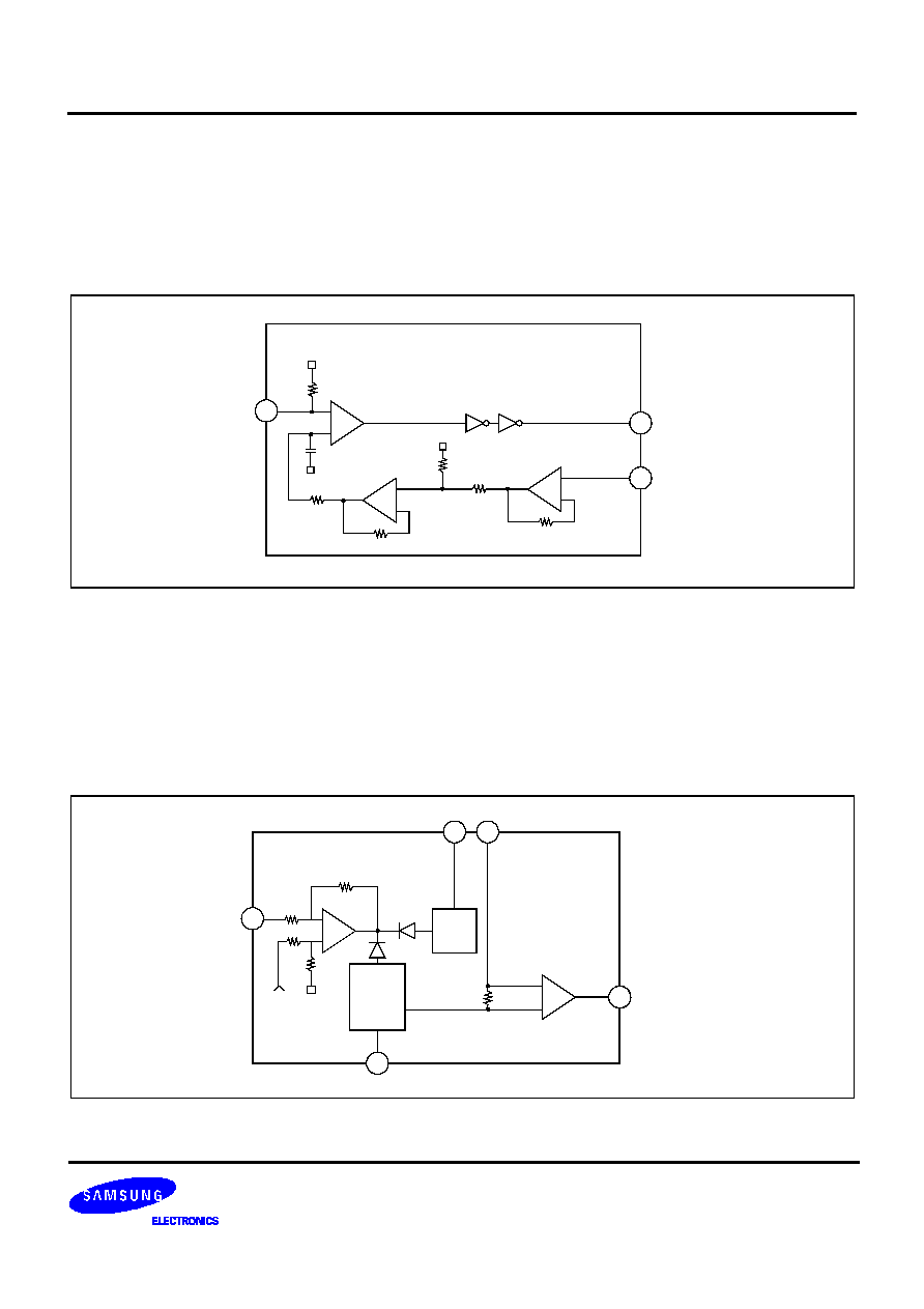
RF AMPLIFIER
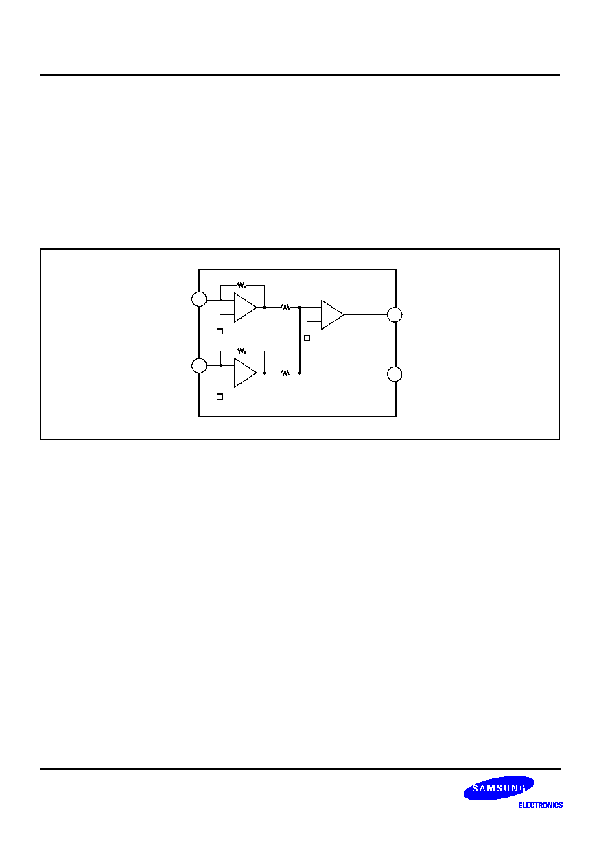
The optical currents input through pins PD1(A+C) and PD2(B+D) are converted into voltages through I-V amp, and
they are added to RF summing amp. The voltage, converted from the photo diode (A+B+C+D) signal, is output
through RFO (pin74) and the eye pattern can be checked at this pin.
FOCUS ERROR AMP
The output of the focus error amp is the difference between I-V amp(1) output VA and
RF I-V amp(2) output VB. The focus error bias voltage applied to the (+) of focus error amp can be changed by
output voltage of D/A converter as shown in diagram, so that the offset of focus error amp can be adjusted
automatically by controlling 5 bits counter switches. Focus error bias can be adjusted from the range of +100mV --
-100mV by connecting the resistor on pin 63 (FEBIAS).
Figure 1. RF Amplifier Circuit
65
66
-
+
-
+
74
-
+
73
PD1
PD2
RFO
RF-
58K
10K
VA
I-V amp(1)
VC
58K
10K
VB
I-V amp(2)
VC
VC
RF summing amp

RF AMP & SERVO SIGNAL PROCESSOR
S1L9223B01
19
TRACKING ERROR AMP
The optical currents detected from the side photo diode (E and F) pf pick-up are input to the E and F pin and
converted into voltage signals by E I-V and F I-V amp. The output of tracking error amp generates the difference
between E I-V AMP and F I-V AMP voltage output.
The E-F balance can be adjusted by modifying the gain of E I-V AMP, and the tracking gain can be adjusted
automatically by controlling the peak voltage at pin TE2 by MICOM program.
Figure 2. Focus Error Amplifier Circuit
Figure 3. Tracking Error Amplifier Circuit
63
-
+
59
-
+
-
+
sev-stopb
FEBIAS
sev-stop
32K
32K
<5 Bit Counter>
3K
X1
X2
X4
X8
X16
164K
FE1
160K
4K
fcmpo
vc
FEBIAS
fe-stopb
SW1
VB >
VA >
fe-stopb
1.
VA and VB refer to output signal of PD1 and PD2 I/V amp.
2.
sev-stopb,sev-stop,fe-stopb and fcmpo are internal signals
67
-
+
68
79
I-V AMP
I-V AMP
54
55
Balance
F
E
EI
GAIN_UP/DOWN
BAL < 4 : 0 >
GAIN < 3 : 0 >
TE1
LPFT
13K
75
K
220K
1
10K
56K
27K
13K
16K
7.
5K
3.
3K
1.
5
K
-
53
TE2
Window Comp
Gain
Window Comp
TRCNT
31
30
ISTAT
S1L9223B01
RF AMP & SERVO SIGNAL PROCESSOR
20
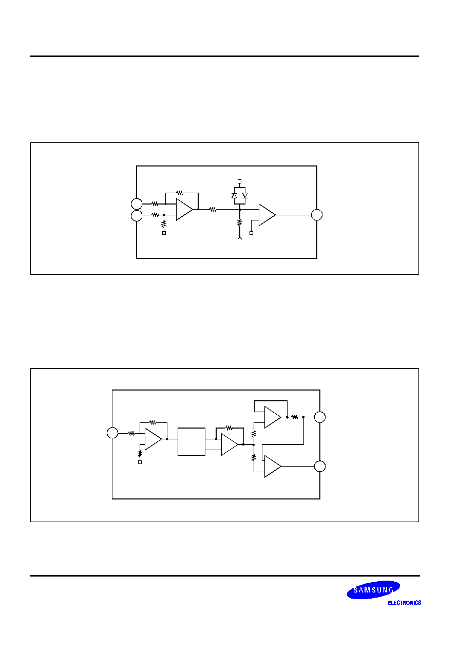
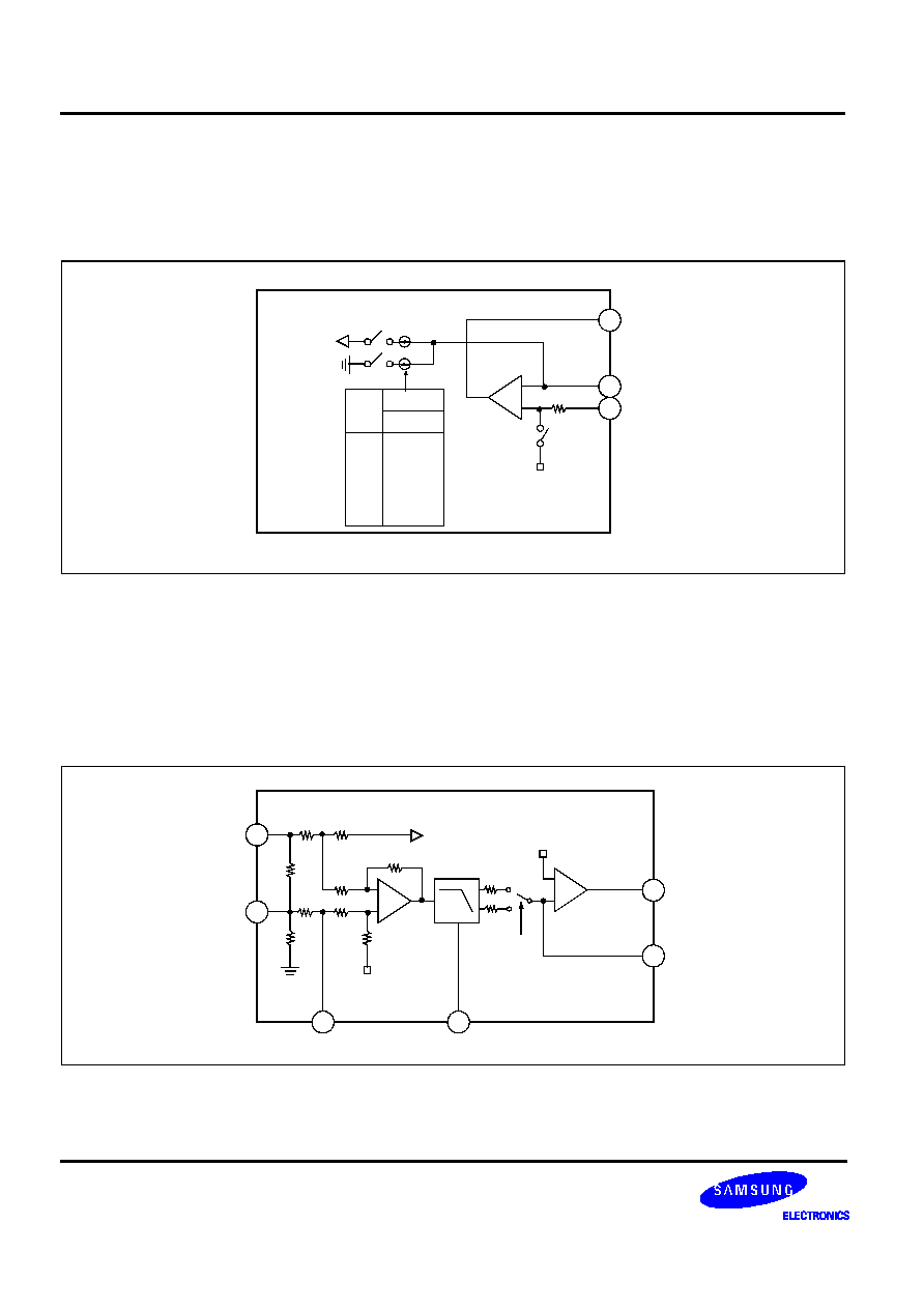
FOCUS OK CIRCUIT
The FOK is the output. The focus OK circuit generates a timing window to enable focus servo operation from focus
search status. When the difference of the RFO (pin74) signal and DC coupled signal IRF (pin75) are above the
predefined voltage the Focus OK circuit output (pin40) becomes active (High output). The predefined voltage is -
0.39V
MIRROR CIRCUIT
IRF signal is amplified by the mirror amp, and the peak and bottom component of amplified signal are detected by
peak and bottom hold circuit. The peak hold circuit covers traverse signal of up to 100KHz component and bottom
hold circuit capable of covering the envelope frequency of disc rotation. The time constant for the mirror hold must
be sufficiently larger than that of the traverse signal.
Figure 5. Mirror Circuit
Figure 4. Focus OK Circuit
74
75
-
+
-
+
40
RFO
IRF
FOK
40K
40K
40K
57K
90K
VC+0.625V
75
-
+
1
IRF
Peak and
Bottom
Hold
-
+
39
-
+
-
+
17K
38K
19K
2.5K
96K
17K
1.5K
MIRROR
MCP
RF AMP & SERVO SIGNAL PROCESSOR
S1L9223B01
21
EFM COMPARATOR
The EFM comparator converts a RF signal into a binary signal.
Because the asymmetry generated due to variations in disc manufacturing can not be eliminated by the AC
coupling alone, this circuit uses to control reference voltage of EFM comparator for eliminating asymmetry.
Figure 6. EFM Comparator & Asymmetry Circuit
DEFECT CIRCUIT
The RFO signal bottom, after being inverted, is held with two time constants of long and short.
The short time-constant bottom hold is done for a disc mirror defect more than 0.1msec, the long time-constant
bottom hold is done with the mirror level prior to the defect. By differentiating this with a capacitor coupling and
shifting the level, both signals are compared to generate the mirror defect detection signal.
Figure 7. Defect Circuit
77
33
RFI
32
-
+
ASY
EFM
-
+
-
+
40K
19K
100K
100K
20K
85K
74
RFO
41
-
+
SSTOP/DFCT
2
BOTTOM
HOLD
5
-
+
4
DCC1
DCC2
DCB
75K
37.5K
28K
75K
VC+0.6254V
43K
DFCT
BOTTOM
HOLD

S1L9223B01
RF AMP & SERVO SIGNAL PROCESSOR
22
APC (AUTO POWER CONTROL) CIRCUIT
The laser diode has large negative temperature characteristic in its optical output when driven with a constant
current on laser diode. Therefore, the output on processing monitor photo diode, must be a controlled current for
getting regular output power, thus the APC (Auto Power Control) circuit is composed.
Figure 8. APC Circuit
AGC STABILITY CIRCUIT
The AGC block is the function used to maintain the constant level of RF peak to peak voltage. After the operation of
RF envelop detection and comparing with reference voltage, RFO level is kept stable in 1Vp-p, and input to EFM
Slice.
Figure 9. AGC Block
69
PD
70
-
+
LD
-
+
43.5K
150K
5.5K
150K
150K
PN (From MICOM command)
300K
LDON
0.75K
(From MICOM command)
1.25V
75
VCA
EQUALIZE
78
76
IRF
EQC
EQO

RF AMP & SERVO SIGNAL PROCESSOR
S1L9223B01
23
POST FILTER
The adjustment of audio output gain and the integration of possible de-emphasis output are executed by this circuit.
This block has amps of 2 channel for gain and filter setting and mute pin for audio signal muting.
Figure 10. Post Filter Circuit
CENTER VOLTAGE GENERATION CIRCUIT
The center voltage is generated by voltage divide using resistor.
Figure 11. Center Voltage Generation Circuit
-
+
-
+
12
-
+
10
-
+
15
-
+
13
19
25K
25K
CH2I
GC2I
GC1I
CH1I
CH2O
GC2O
GC1O
CH1O
MUTEI
VCC
-
+
VR
30K
30K
VCC
71

S1L9223B01
RF AMP & SERVO SIGNAL PROCESSOR
24
SERVO BLOCK
FOCUS SERVO BLOCK
When defect is "H" (the defect signal is detected), the focus servo loop is muting in case of focus phase
compensation. At this time, the focus error signal is output through the low pass filter formed by connecting a
capacitor (0.1
µ
F) and a built-in 470K
resistor to the FDFCT pin (pin 60). Accordingly, the focus error output is held
at the error value just before defect error during defect occurring. The peak frequency of focus loop phase
compensation is at about 1.2KHz when the resistor connected to FSET pin (pin 6) is 510K
, and it is inversely
proportional to the resistor connected to the FSET pin. While the focus search is operating, the FS4 switch is on
and then the focus error signal is isolated, accordingly the focus search signal is output by FEO pin (pin 48). When
the FS2 switch is on (focus on), the focus servo loop is on and the focus error signal from FE2 pin (pin 58) is output
through the focus servo loop.
Figure 12. Focus Servo Block
58
-
+
60
28
27
Focus Phase
Compensation
26
47
-
+
-
+
-
+
-
+
3
3.6K
60K
FZCI
FE2
470K
DFCTI
20K
48K
FS4B
130K
FGD
FS3
46K
580K
FS3
470K
40K
FS2B
FLB
FRCH
50K
10K
3.6K
FS1
92K
40K
FE-
FEO
VC
FSCMPO
48
FDFCT
PS
4 3
X1
X2
X3
X4
0 0
0 1
1 0
1 1
6
FSET
X1
X2
X3
X4

RF AMP & SERVO SIGNAL PROCESSOR
S1L9223B01
25
TRACKING SERVO BLOCK
During detection of defect, the tracking error signal is output through the tracking servo loop after passing the low
pass filter formed by connecting a capacitor (0.1
µ
F) and a built-in 470K
resistor to the TDFCT pin (pin57) in case
of tracking phase compensation. The value of tracking gain up/down can be controlled by TGU and TG2 pin. The
peak frequency of tracking loop phase compensation, the dynamic range and offset of OP AMP can be adjusted by
changing the value of resistor connected to FSET pin same as focus loop. In case of unstable status of actuator
after jumping, the ON/OFF of tracking loop is controlled by TM7 switch of break circuit.
After 10-track jumping, servo circuit gets out of the liner range and actuator's tracking becomes occasionally
unstable. Hence unnecessary jumping with many tracking error should be prevented.
Figure 13. Tracking Servo Block
-
+
53
57
61
62
TRACKING
PHASE
COMPENSATION
49
50
TE2
470K
TDFCT
680K
TGU
TG2
470K
20K
10K
110K
82K
680K
66PF
10K
90K
FSET
TE-
TG1
TG1
TM1
TG2
TM7
TM3
TM4
DFCTI
6
TEO
S1L9223B01
RF AMP & SERVO SIGNAL PROCESSOR
26
SLED SERVO BLOCK
The moving of pick-up is controlled by tracking servo output through a low pass filter.
The sled kick voltage is output for track jump operation.
Figure 14. Sled Servo Block
SPINDLE SERVO BLOCK
The 20K
resistor and 0.33uF capacitor form the 200Hz low pass filter, and the carrier component of spindle servo
error signals is eliminated. In CLV-S mode, SMEF becomes "L" and pin 25 low pass filter fc lowers, strengthening
the filter further. The characteristics of high frequency phase compensation in focus tracking servo and the
characteristics of cut off frequency in CLV low pass filter are tested by FSET pin.
Figure 15. Spindle Servo Block
-
+
43
44
42
PS
4 3
X 1
X 2
X 3
X 4
0 0
0 1
1 0
1 1
SLO
SL-
SL+
TM6
TM7
TM2
-
+
24
46
45
23
25
-
+
6
SMON
SMDP
22K
22K
15K
20K
15K
220K
220K
220K
220K
50K
100K
SMEF
FSET
SPDL-
SPDLO
Double
speed

RF AMP & SERVO SIGNAL PROCESSOR
S1L9223B01
27
DIGITAL BLOCK
DESCRIPTION
Digital block is transferred serial data by MICOM and 8-bit serial data is converted to parallel data by serial to
parallel register. This data is decoded by latch signal. The status output of focus servo, tracking servo and sled
servo system,etc. It is determined by each data. The auto-sequence function process 2 -- 4 MICOM command by
one auto-sequence command.
Figure 16. CPU Serial Interface Timing Chart
Item
Symbol
Min
Typ
Max
Unit
Clock Frequency
fck
-
-
1
MHz
Clock Pulse Width
fwck
500
-
-
ns
Hold Time
tsu
500
-
-
ns
Setup Time
tn
500
-
-
ns
Delay Time
td
500
-
-
ns
Latch Pulse Width
twl
1000
-
-
ns
MDATA
MCK
twck
twck
tsu
tsn
D0
D1
D2
D3
D4
D5
D6
D7
MLT
twl
td

S1L9223B01
RF AMP & SERVO SIGNAL PROCESSOR
28
MICOM COMMAND SET
Focus Control ($0X)
This command consists of 8 bits data and expressed by two hexa $0X.
FS4, FS3, FS2, FS1: internal switch for focus control
∑
Focus Search Operation (FS2,FS1)
$02: FS2 switch become off and the value of servo output pin is as below.
(10
µ
A-5
µ
A)*50k*(feedback Resistor/50k)
$03: If FS1 switch is 1, the current supply is cut off and the discharge is performed.
The waveform is as below and the time constant is determined by internal resistor 50K and external Cap.
Item
Hexa
Address
Data
ISTAT Out
D7
D6
D5
D4
D3
D2
D1
D0
Focus
Control
$0X
0
0
0
0
FS4
Focus On
FS3
Gain Down
FS2
Search On
FS1
Search Up
FZC
Tracking
Control
$1X
0
0
0
1
Anti Shock
Brake On
TG2
Gain Set
TG1
Gain Set
A.S
Tracking
Mode
$2X
0
0
1
0
Tracking Mode
Sled Mode
TZC
Select
$3X
0
0
1
1
PS4
Focus
Search+2
PS3
Focus
Search+2
PS2
Sled Kick+2
PS1
Sled Kick+1
STOP
Auto
Sequence
$4X
0
1
0
0
AS3
AS2
AS1
AS0
/BUSY
R
A
M
S
E
T
Blind/
overflow
$5X
0
1
0
1
0.18ms
0.09ms
0.045ms
0.022ms
Hi-Z
Break
0.36ms
0.18ms
0.09ms
0.045ms
Kick
$6X
0
1
1
0
11.6ms
5.80ms
0.09ms
0.045ms
2N
jump
$7X
0
1
1
1
64
32
16
8
move
(M)
128
64
32
16
Auto Adj.
$8XX
1
0
0
0
Offset, Balance, Gain, APC Control
-
Speed
$FX
1
1
1
1
$F0: Normal Speed
$F3: Double Speed
-
D7
D6
D5
D4
D3
D2
D1
D0
ISTAT
0
0
0
0
FS4
FS3
FS2
FS1
FZC
RF AMP & SERVO SIGNAL PROCESSOR
S1L9223B01
29
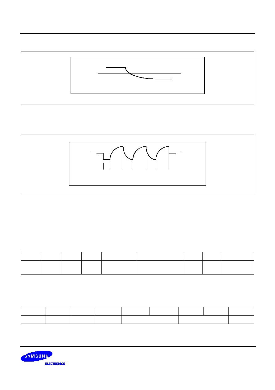
Figure 17. Waveform at Pin 3 When FS1 Is Switched from 0 to 1
The waveform of servo output pin according to FS1 and FS2 switches is as below.
Figure 18. Focus Search Waveform at Pin 48 by $02 and $03
FS4 is switch for on/off control of focus servo loop
$00: Focus servo off
$08: Focus servo on
Tracking Control ($1X)
This command is used for tracking loop gain control, break circuit and anti-shock on/off control.
TG2 and TG1 are internal switch for tracking gain set.
Tracking mode ($2X)
This command is used for tracking and sled servo on/off and jump for searching track.
D7
D6
D5
D4
D3
D2
D1
D0
ISTAT
0
0
0
1
Anti shock
on/off
Break circuit
on/off
TG2
TG1
Anti shock
D7
D6
D5
D4
D3
D2
D1
D0
ISTAT
0
0
1
0
Tracking control
Sled control
TZC
0V
$00 02
03
02
03
02
03
00
S1L9223B01
RF AMP & SERVO SIGNAL PROCESSOR
30
<Tracking control & Sled control>
Peak value set ($3X)
This command is used for the peak value setting of focus search and sled kick.
D0, D1: Sled kick
D2, D3: Focus search peak value
Auto Sequencer command ($4X)
This command is used for reducing control time and replacing several command by one auto- sequence command.
∑
Auto sequencer mode is performed from the first falling edge of WDCK clock after the falling of the latch pulse.
∑
Auto sequencer does not carry out tracking gain up, brake, anti-shock and focus gain down.
∑
MICOM checks ISTAT pin (/BUSY) and sends to $40 command to reset preceding auto sequencer status
RAM Set ($5X -- $7X)
The value of RAM set is somewhat different to the actual count and the initial value is like below
D3
D2
Tracking mode
D1
D0
Sled mode
0
0
Tracking servo off
0
0
Sled servo off
0
1
servo on
0
1
servo on
1
0
Forward jump
1
0
Forward kick
1
1
Reverse jump
1
1
Reverse kick
Hexa
AS3
AS2
AS1
AS0
Remark
Cancel
$40
0
0
0
0
Reset
Auto focus
$47
0
1
1
1
-
1 Track jump
$48
$49
1
1
0
0
0
0
0
1
Forward
Reverse
10 Track jump
$4A
$4B
1
1
0
0
1
1
0
1
Forward
Reverse
2N track jump
$4C
$4D
1
1
1
1
0
0
0
1
Forward
Reverse
M track move
$4E
$4F
1
1
1
1
1
1
0
1
Forward
Reverse
Item
Initial value
Actual Count Value
Blind
$55
Set value +4 -- 5 WDCK clock
overflow, Brake
Set value +3 WDCK clock
Kick
$67
Set value +5 WDCK clock
2N, M Track jump
$7E
Set value +3 WDCK clock
RF AMP & SERVO SIGNAL PROCESSOR
S1L9223B01
31
AUTO ADJUSTMENT COMMAND
This command is used for auto control of offset, balance, gain adjustment and reference voltage setting. This
command is also in control of on/off and sub type of laser diode and test or set mode.
TRACKING BALANCE ($800 -- $81F)
TRACKING GAIN ($820 -- $83F)
TRACKING BALANCE & GAIN WINDOW LEVEL SETTING
NOTE: The tracking balance and gain window level is set by D2,D3 data and the value has two kinds of window levels set
TRACKING BALANCE WINDOW LEVEL
TRACKING GAIN WINDOW LEVEL
FOCUS LOOP OFFSET ADJUSTMENT START COMMAND ($841, $842)
This command is used for adjusting focus error bias and removing focus servo offset.
It is executed during laser diode off.
Item
Hexa
Data (5bits)
Initial value
ISTAT (pin31)
TRCNT (pin30)
Tracking balance
$800 -- $81F
D4 -- D0
$81F
BAL
TRCNT
Item
Hexa
Data 5bits)
Initial value
ISTAT (pin31)
TRCNT (pin30)
Tracking gain
$820 -- $83F
D4 -- D0
$820
GAIN
TGL
Item
Hexa
D3
D2
D1
D0
Initial value
window level setting
$84X
gain
balance
0
0
$840
D2 Data
0
1
Tracking balance window level
-
10 to +15 mV
-
20 to +20 mV
D3 Data
0
1
Tracking gain window level
250 to 400 mV
150 to 300 mV
Hexa command
meaning
$841
Focus error bias adjustment start command
$842
Focus servo offset cancel adjustment start command

S1L9223B01
RF AMP & SERVO SIGNAL PROCESSOR
32
APC CIRCUIT OPERATION AND INTERRUPTION ON/OFF SETTING CONDITION ($85X)
This command is used for setting of laser diode on/off, sub type (P_sub or N_sub) of laser diode and interruption
countermeasure circuit on/off.
Time setting for Interruption countermeasure circuit on/off
FOCUS SERVO OFFSET RESET COMMAND AND SET MODE COMMAND (86X)
This command is used for set and release before focus servo loop offset adjustment and mode change.
NOTES:
1.
The set mode command is sent by MICOM right after tracking gain is tuned.
2.
The ISTAT pin is outputted the internal status of $00 ~ $7X command.
DIRECT COMMAND (DIRC) AND FOCUS BIAS RESET COMMAND ($87X)
This command is used for direct 1 track jump on/off setting and focus bias adjustment set and release
Item
Hexa
D3
D2
D1
D0
Initial value
APC &
Interruption on/off
condition
$85X
LD on/off
0: On
1: Off
Sub-type
0: N_sub
1: P_sub
Interruption ON/OFF
and time setting
$858
D1
D0
Meaning
0
0
Countermeasure circuit on for all mirror signal
0
1
Countermeasure circuit on up to 20kHz mirror signal
1
0
Countermeasure circuit off
1
1
Countermeasure circuit on up to 10kHz mirror signal
Item
Hexa
D3
D2
D1
D0
Set mode & Focus servo
offset reset command
$86X
0: offset release
1: offset reset
option(Pin41 output)
0: Defect
1: SSTOP
1
1
Item
Hexa
D3
D2
D1
D0
DIRC
& focus bias reset
$87X
0: DIRC On
1:DIRC Off
0: reset
1: reset release
X
X

RF AMP & SERVO SIGNAL PROCESSOR
S1L9223B01
33
THE EXAMPLE OF ADJUSTMENT FREE ALGORITHM
FOCUS ERROR BIAS & SERVO OFFSET CANCEL ADJUSTMENT
Figure 19. Focus Error Bias & Servo Offset Cancel Adjustment Flow Chart
Focus_RF_Offset Adjustment
[Command:841]
ISTAT
Check
L--> H
Finish
[RF CNT value Latch]
Focus_Servo_Offset
Adjustment [Command:842]
ISTAT
Check
L--> H
Finish
[Servo value Latch]
yes
Increment Count
no
Increment Count
no
yes
Time Max
100msec
Time Max
100msec
5bit Counter 17mV/Bit
Tuning range: + 260mV
4bit Counter
40mV/Bit
tuning range : + 280mV

S1L9223B01
RF AMP & SERVO SIGNAL PROCESSOR
34
TRACKING BALANCE ADJUSTMENT
Figure 20. Tracking Balance Adjustment Flow Chart
TRACKING GAIN ADJUSTMENT
Figure 21. Tracking Gain Adjustment Flow Chart
Balance adjustment Range window
setting + 20mv, + 15mv setting
ISTAT
Check
L--> H
Finish
[RF CNT value Latch
NO
$844
ISTAT
Check
L--> H
MICOM Balance
5Bit adjustment
Command Up
YES
NO
YES
$800 ~ $81F
Gain adjustment range
setting Command
ISTAT
Check
L--> H
Gain adjustment finish
NO
5-bit Gain Adjustment
Command
YES
$848
$820 ~ $83F
TOC READ
RF AMP & SERVO SIGNAL PROCESSOR
S1L9223B01
35
APPLICATION CIRCUIT
47K
1
2
3
4
5
6
7
8
9
10
11
12
13
14
15
16
17
18
19
20
21
22
23
24
25
26
27
28
29
30
31
32
33
34
35
36
37
38
39
40
64
63
62
61
60
59
58
57
56
55
54
53
52
51
50
49
48
47
46
45
44
43
42
41
80
79
78
77
76
75
74
73
72
71
70
69
68
67
66
65
S1L9223B01
MCP
DCB
FRSH
DCC2
DCC1
FSET
VDDA
VCCP
GC2I
GC2O
CH2I
CH2O
CH1O
CH1I
GC1O
GC1I
RRC
VSSP
MUTEI
ISET
VREG
WDCK
SMDP
SMONSM
EF
FL
B
FS
3
FG
D
LO
C
K
T
RCNT
IS
T
A
T
ASY
EF
M
VSSA
MC
K
MD
A
T
A
ML
T
R
E
SET
M
I
RRO
R
FO
K
DVEE
FEBIAS
TG2
TGU
FDFCT
FE1
FE2
TDFCT
DVDD
LPFT
TE1
TE2
TZC
ATSC
TEO
TE-
FEO
FE-
SPDLO
SPDL-
SL-
SLO
SL+
SSTOP
GND
EI
EQ
C
RF
I
EQ
O
IRF
RF
O
RF
-
VCC
VR
LD
PD
E
F
PD2
PD1
+
152p
103p
333p
103p
510K
+
+
+
+
+
+
VC
GND
VCC
VC
C
1K
3.3uF
A
B
C
D
E
F
VC
C
100uF
22K
33uF
22K
4p
F
47
2p
10
3
p
1uF
4.7uF
VC
C
VCC(POST)
27K
4.
7u
F
1
50p
27
K
331p
5.
6K
5.
6K
5.
6K
5.
6
K
4.
7uF
27K
GND (POST)
from MICOM
180K
from DSP
8.2K
1M
333p
0.47uF
104p
104
p
fr
o
m
D
S
P
to
M
O
C
O
M
to
M
O
C
O
M
0.
47uF
10
3p
100K
to
D
S
P
fr
o
m
M
O
C
O
M
to KA9258D
683
p
1
03p
56K
47
K
10uF
120
K
391p
120K
10
0K
to KA9258D
to KA9258D
to KA9258D
333p
1K
22
2p
10
0K
15
0K
103p
104p
VC
C
104p
222p
10K
10K
1
04p
GN
D
fro
m
pi
ck-
up
+
to
pick-u
p
10
2
+
33uF
+
331p
150
p
27K
152p
152p
5.6K
5.6K
from DAC CH1
from DAC CH2
CH1 out
CH2 out
+
4.7uF
from DSP(SMDP)
from DSP(SMON)
from DSP(SMSD)
+
from DSP(SMEF)
+
12K
fr
o
m
M
O
C
O
M
fr
o
m
M
O
C
O
M
fr
o
m
M
O
C
O
M
to
M
O
C
O
M
fr
o
m
d
e
ck
15K
+
39K
0.47uF
102p
104p
+
S1L9223B01
RF AMP & SERVO SIGNAL PROCESSOR
36
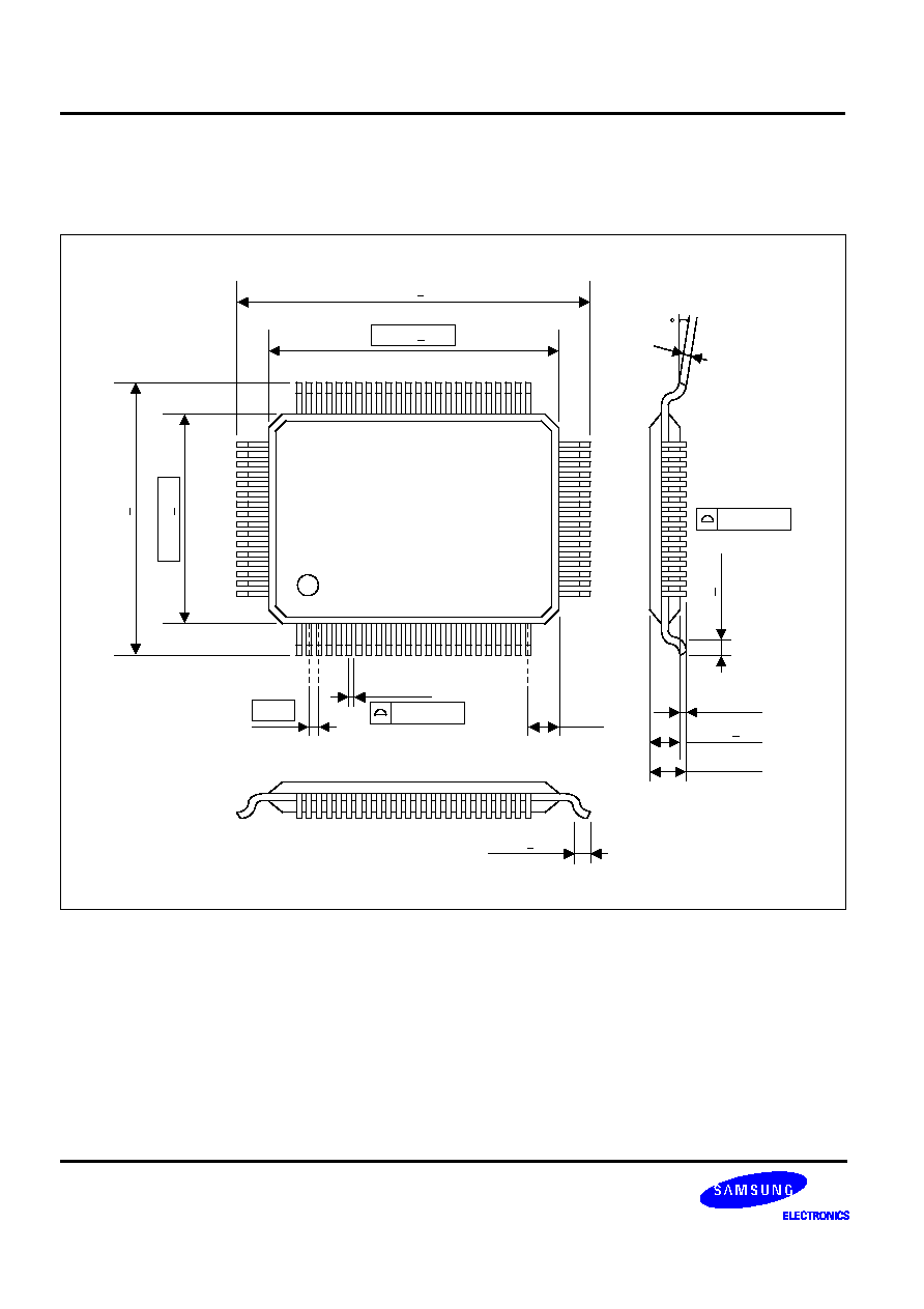
PACKAGE DIMENSION
80-QFP-1420C
#80
20.00
+ 0.20
23.90
+ 0.30
14.00
+
0.20
17.90
+
0.30
#1
0.80
0.35
+ 0.10
0.15 MAX
(0.80)
0.15
+ 0.10
- 0.05
0-8
0.10 MAX
0.80
+
0.20
0.05 MIN
2.65
+ 0.10
3.00 MAX
0.80
+ 0.20