 | –≠–ª–µ–∫—Ç—Ä–æ–Ω–Ω—ã–π –∫–æ–º–ø–æ–Ω–µ–Ω—Ç: S1L9225 | –°–∫–∞—á–∞—Ç—å:  PDF PDF  ZIP ZIP |
RF AMP & SERVO SIGNAL PROCESSOR
S1L9225X
1
INTRODUCTION
As a pre-signal & servo signal processor for the DISC-MAN, S1L9225X is a low
voltage, low consumption current IC that can read CD-RW, and CD-R discs and
can be applied to various products, such as the CDP/VCD/CD-MP3 for the
DISC-MAN. It is a hard-wired free-adjustment servo, which automatically
controlled the control point of the pre-signal portion.
FEATURES
∑
RF amplifier (CD, CD-R, CD-RW applicable)
∑
Gain setting & monitoring for the CD-R, CD-RW DISC
∑
Focus error amp & Febias adjustment
∑
Tracking error amp & balance, gain adjustment
∑
FOK, defect, mirror detect
∑
Center voltage amplifier
∑
APC (Automatic Power Control)
∑
APC laser controller (Controlled by Tracking Summing Signal)
∑
RF AGC & EQ control (AGC Level Control Compatible)
∑
Enhanced EFM slice (Double Asymmetry Method)
∑
Focus servo loop & offset adjustment
∑
Tracking servo loop & offset adjustment
∑
Sled servo loop
∑
Spindle servo loop
∑
Auto-sequence
∑
Fast search mode (1 - 36000 track jump)
∑
Interruption countermeasure
∑
Focus & Tracking servo muting controlled by EFM duty check
∑
RF peaking prevention system by EFM duty check
∑
Focus, tracking, spindle loop pole move option
∑
Operating voltage 2.7V
3.3V
∑
Power saving mode
<Notice> LPC Control used by side beam signal, it related to pick-up assurance.
When used pick-up, the specification is present extra.
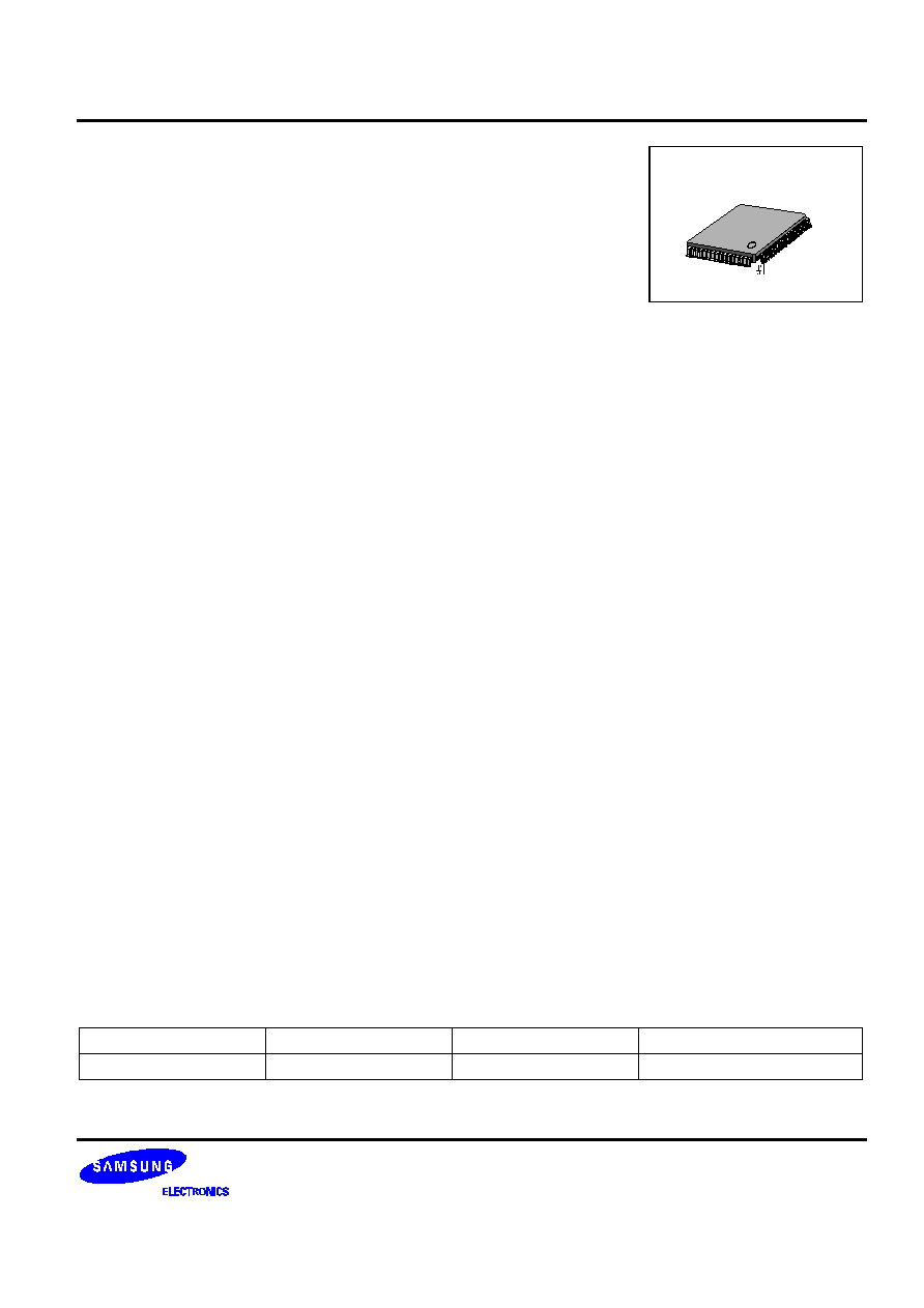
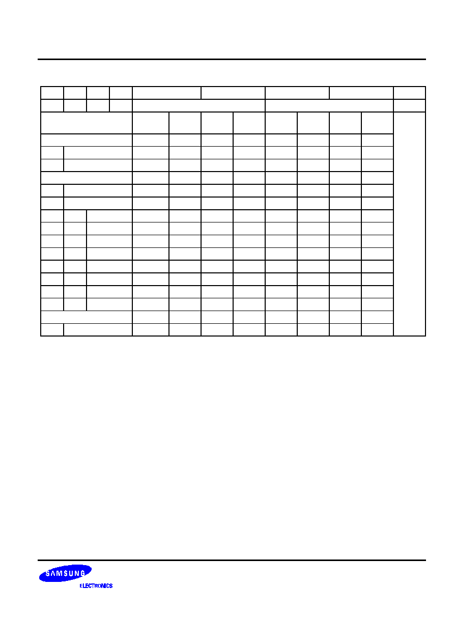
ORDERING INFORMATION
Device
Package
Supply Voltage
Operating Temperature
S1L9225X01
Q0R0
64-LQFP-1414
2.7V
3.3V
-20
∞
C
+75
∞
C
64-LQFP-1010
S1L9225X
RF AMP & SERVO SIGNAL PROCESSOR
2
BLOCK DIAGRAM
1
2
3
4
5
6
7
8
9
10
11
12
13
14
15
16
48
47
46
45
44
43
42
41
40
39
38
37
36
35
34
33
64
63
62
61
60
59
58
57
56
55
54
53
52
51
50
49
17
18
19
20
21
22
23
24
25
26
27
28
29
30
31
32
RF AGC &
EQ Control
Focus OK Detect
Defect Detect
Mirror Gen
Center
Voltage
APC. Laser
Control &
LPC
Tracking Servo Loop
- Gain & Phase
Compensation
- Track Jump
- Offset Adjust
- TZC Gen.
Tracking
Error
(RW) I/V
AMP
RF & Focus
Error (CD-RW)
I/V AMP
Hardware Logic
- Auto-Sequencer
- Fast Search
- Febias, Focus Servo,
Tracking Offset ADJ.
- Tracking Balance & Gain
Adjust
- Interruption Detect
- EFM Muting System
Sled Servo
& Kick Gen
Spindle
Servo LPF
EFM
Comparator
Micom Data Interface Logic Decoder
Focus Servo Loop
- Gain & Phase
Compensation
- Focus Search
- Offset Adjust
- FZC Gen.
EQO
EFMI
DCC1
DCC2
MCP
DCB
VSSA/GND
FRSH
FSET
FLB
FGD
FDFCT
FSE0
FSI
ATSCO
TGU
PD
LD
LPFT2
LPFT1
TEIO
TZC
ATSC
TEO
TEM
SLP
SLO
SLM
FEO
FEM
SPDLO
SPDLM
EQI
RFO
RFM
RFM2
TESO
LPC
LPB
EQC
VCC
VREF
PDE
PDF
PDD
PDB
PDC
PDA
VDDA
ISTAT2
ISTAT1
MCK
MDATA
MLT
RESET
WDCK
CLVI
LOCK
ASY
EFM2
EFM
SSTOP
VSS
VDD
EQO

RF AMP & SERVO SIGNAL PROCESSOR
S1L9225X
3
APPLICATION DIAGRAM
S1L9225X
To Micom
From Micom
120K
1
2
3
4
5
6
7
8
9
10 11 12 13 14 15 16
64
63
62
61
60
59
58
57
56
55
54
53
52
51
50
49
48 47 46 45 44 43 42 41 40 39 38 37 36 35 34 33
17
18
19
20
21
22
23
24
25
26
27
28
29
30
31
32
PD
LD
LPFT2
LPFT1
TEIO
TZC
ATSC
TEO
TEM
SLP
SLO
SLM
FEO
FEM
SPDLO
SPDLM
VDDA
ISTAT2
ISTAT1
MCK
MDATA
MLT
RESET
WDCK
CLVI
LOCK
ASY
EFM2
EFM
SSTOP
VSS
VDD
EQO
EFMI
DCC1
DCC2
MCP
DCB
VSSA/GND
FRSH
FSET
FLB
FGD
FDFCT
FSEO
FSI
ATSCO
TGU
EQO
821
47pF
333
103
103
4.7uF
104
104
104
102
104
From Micom
To Micom
From Micom
From Micom
From DSP
333
474
1M
20K
8.2K
FSW
SMDS
SMDP
10K
From DSP
474
103
To DSP
From_Pick-up
47K
381
56K
103
15K
100K
39K 474
120K
683
10uF
222
333
150K
103
103 103
100uF
3V
22
1uF
A
EQI
RFO
RFM
RFM2
TESO
LPC
LPB
EQC
VCC
VREF
PDE
PDF
PDD
PDB
PDC
PDA
B
C
D
E
F
500
100
3V
1K
3.6uF
33uF
683
2.2uF
82pF
12pF
22K
8pF
153

S1L9225X
RF AMP & SERVO SIGNAL PROCESSOR
4
PIN CONFIGURATION
S1L9225X
1
2
3
4
5
6
7
8
9
10
11
12
13
14
15
16
48
47
46
45
44
43
42
41
40
39
38
37
36
35
34
33
64
63
62
61
60
59
58
57
56
55
54
53
52
51
50
49
17
18
19
20
21
22
23
24
25
26
27
28
29
30
31
32
EQO
EFMI
DCC1
DCC2
MCP
DCB
VSSA/GND
FRSH
FSET
FLB
FGD
FDFCT
FSE0
FSI
ATSCO
TGU
PD
LD
LPFT2
LPFT1
TEIO
TZC
ATSC
TEO
TEM
SLP
SLO
SLM
FEO
FEM
SPDLO
SPDLM
EQI
RFO
RFM
RFM2
TESO
LPC
LPB
EQC
VCC
VREF
PDE
PDF
PDD
PDB
PDC
PDA
VDDA
ISTAT2
ISTAT1
MCK
MDATA
MLT
RESET
WDCK
CLVI
LOCK
ASY
EFM2
EFM
SSTOP
VSS
VDD
EQO

RF AMP & SERVO SIGNAL PROCESSOR
S1L9225X
5
PIN DESCRIPTION
Table 1. Pin Description
Pin No
Symbol
I/O
Description
1
EQO
O
RF equalizer output
2
EFMI
I
EFM slice input. (input impedance 47K)
3
DCC1
O
Time constant connection output to detect defects
4
DCC2
I
Time constant connection input to detect defects
5
MCP
I
CAP connection terminal for mirror hold
6
DCB
I
CAP terminal to limit defect detection
7
VSSA/GND
G
RF, servo ground
8
FRSH
I
CAP connection terminal for focus search
9
FSET
I
Filter bias for focus, tracking, spindle
10
FLB
I
CAP terminal to make focus loop rising low band
11
FGD
I
Terminal to change the high frequency gain of the focus loop
12
FDFCT
I
CAP connection terminal to integrate the focus error
13
FSEO
O
Focus error output
14
FSI
I
Focus servo input
15
ATSCO
O
Shock level detect output (shock: L: state)
16
TGU
I
Time constant connection to change the high frequency gain of the
tracking loop.
17
VDDA
P
Power supply for the servo
18
ISTAT2
O
Internal status output pin (FOK, TRCNT)
19
ISTAT1
O
Internal status output pin
20
MCK
I
Micom clock pin
21
MDATA
I
Data input pin
22
MLT
I
Data latch input pin
23
RESET
I
Reset input pin
24
WDCK
I
88.2kHz input terminal from DSP
25
CLVI
I
Control output input terminal of DSP spindle
26
LOCK
I
Sled run away prevention pin (L: sled off and tracking gain up)
27
ASY
I
Auto asymmetry control input terminal
28
EFM2
O
Output for EFM pulse integration
29
EFM
O
EFM output terminal for RFO slice (to DSP)
30
SSTOP
I
PICK UP's maximum lead-in diameter position check pin
31
VSS
G
Digital ground
32
VDD
P
Digital power

S1L9225X
RF AMP & SERVO SIGNAL PROCESSOR
6
Table 1. Pin Description (Continued)
Pin No
Symbol
I/O
Description
33
SPDLM
I
Spindle amp inverting input pin
34
SPDLO
O
Spindle amp output pin
35
FEM
I
Focus servo amp inverting input pin
36
FEO
O
Focus servo amp output pin
37
SLM
I
Sled servo inverting input
38
SLO
O
Sled servo output
39
SLP
I
Sled servo non inverting input
40
TEM
I
Tracking servo amp inverting input pin
41
TEO
O
Tracking servo amp output pin
42
ATSC
I
Anti-shock input pin
43
TZC
I
Tracking zero crossing input pin
44
TEIO
B
Tracking error output & tracking servo input pin
45
LPFT1
I
Tracking error integration input terminal 1 (automatic control)
46
LPFT2
I
Tracking error integration input terminal 2 (automatic control)
47
LD
O
APC AMP output pin
48
PD
I
APC AMP input pin
49
PDA
I
Photo-diode A/C RF I/V amp1 inverting input pin
50
PDB
I
Photo-diode B/D RF I/V amp2 inverting input pin
51
PDC
I
Photo-diode A/C RF I/V amp1 inverting input pin
52
PDD
I
Photo-diode B/D RF I/V amp2 inverting input pin
53
PDF
I
Photo-diode F with tracking (F) I/V amp inverting input pin
54
PDE
I
Photo-diode E with tracking (E) I/V amp inverting input pin
55
VREF
O
(VCC+GND)/2 voltage reference output pin
56
VCC
P
RF part VCC power supply pin
57
EQC
I
AGC_ equalize level control terminal and VCA input connection cap
terminal
58
LPB
I
Laser power level control resistance terminal
59
LPC
I
Laser power control tracking summing signal integration terminal
60
TESO
O
Tracking error summing signal
61
RFM2
I
RF summing amp 2x filter on/off
62
RFM
I
RF summing amp inverting input terminal
63
RFO
O
RF summing amp output terminal
64
EQI
I
RFO dc control input terminal (use by MIRROR, FOK, AGC&EQ
terminals)

RF AMP & SERVO SIGNAL PROCESSOR
S1L9225X
7
MAXIMUM ABSOLUTE RATINGS
Item
Symbol
Rating
Unit
Power supply voltage
V
DD
-0.3
5.5
V
Input supply voltage
V
I
-0.3
V
DD
+ 0.3
V
Operating temperature
T
OPR
-20
75
∞
C
Storage temperature
T
STG
-40
125
∞
C

S1L9225X
RF AMP & SERVO SIGNAL PROCESSOR
8
ELECTRICAL CHARACTERISTICS
Table 2. Electrical Characteristics
No.
Inspection Items
Symbols
Inspection
Block
Spec
Unit
1
Supply current 2.7V
ICCTY
6
10
14
mA
2
RF AMP offset voltage
Vrfo
RF AMP
-85
0
+85
mV
3
RF AMP oscillation voltage
Vrfosc
0
50
100
mV
4
RF AMP voltage gain AC
Grfac
16.2
14.7
17.7
dB
5
RF AMP voltage gain BD
Grfbd
16.2
14.7
17.7
dB
6
RF RHD characteristic
Rfthd
-
-
5
%
7
RF AMP maximum output voltage
Vrfh
2.35
-
-
V
8
RF AMP minimum output voltage
Vrfl
-
-
0.85
V
9
RF CDRW gain AC1
GRWAC1
5.5
7.7
9.9
-
10
RF CDRW gain AC2
GRWAC2
11.0
13.1
16.2
-
11
RF CDRW gain AC3
GRWAC3
18.0
21.3
24.6
-
12
RF CDRW gain BD1
GRWBD1
5.5
7.7
9.9
-
13
RF CDRW gain BD2
GRWBD2
11.0
13.1
16.2
-
14
RF CDRW gain BD3
GRWBD3
18.0
21.3
24.6
-
15
RF IVSEL connection AC
RFSELAC
24
47
70
k
16
RF IVSEL connection BD
RFSELBD
24
47
70
k
17
RF AMP offset conversion 1
Vrfoff1
0
-100
-200
mV
18
RF AMP offset conversion 2
Vrfoff2
-100
-200
-300
mV
19
Focus error offset voltage
VFEO1
Focus Error
-525
-250
-50
mV
20
Focus error auto voltage
VFEO2
Amplifier
-35
0
+35
mV
21
ISTAT state after FEBIAS control
VISTAT1
2.5
-
-
V
22
Focus ERROR voltage gain 1
GFEAC
18
21
24
dB
23
Focus ERROR voltage gain 2
GFEBD
18
21
24
dB
24
Focus ERROR voltage gain difference
GFE
-3
0
+3
dB
25
Focus ERROR AC difference
VFEACP
0
50
100
mV
26
FERR maximum output voltage H
VFEPPH
2.3
-
-
V
27
FERR minimum output voltage L
VFEPPL
-
-
0.4
V
28
AGC max gain
GAGC
AGC_Equalize
16
19
22
dB
29
AGC EQ gain
GEQ
0
1
2
dB
30
AGC normal gain
GAGC2
3
6
9
dB
31
AGC compress ratio
CAGC
0
2.5
5
dB
32
AGC frequency
FAGC
-1.5
0
2.5
dB

RF AMP & SERVO SIGNAL PROCESSOR
S1L9225X
9
Table 2. Electrical Characteristics (Continued)
No.
Inspection Items
Symbols
Inspection
Block
Spec
Unit
33
TERR sum voltage gain SF
GTSF
Tracking Error
16.5
19.5
22.5
dB
34
TERR sum voltage gain SE
GTSE
Amplifier
16.5
19.5
22.5
dB
35
TERR sum voltage gain S2
GTS2
22.5
25.5
28.5
dB
36
TERR gain voltage gain 1
GTEF1
-1.5
0.5
2
dB
37
TERR gain voltage gain 2
GTEF2
1
1.7
2.4
-
38
TERR gain voltage gain 3
GTEF3
1
1.3
1.6
-
39
TERR gain voltage gain 4
GTEF4
1
1.45
1.9
-
40
TERR gain voltage gain 5
GTEF5
1
1.55
2.1
-
41
TERR gain voltage gain 6
GTEF6
1
1.45
1.9
-
42
TERR gain voltage gain 7
GTEF7
1
1.45
1.9
-
43
TERR balance gain
GTEE
10.5
13.5
16.5
dB
44
TERR balance mode 1
TBE1
1.0
1.05
1.1
-
45
TERR balance mode 2
TBE2
1.0
1.05
1.1
-
46
TERR balance mode 3
TBE3
1.0
1.05
1.1
-
47
TERR balance mode 4
TBE4
1.0
1.25
1.5
-
48
TERR balance mode 5
TBE5
1.0
1.20
1.4
-
49
TERR balance mode 6
TBE6
1.0
1.3
1.75
-
50
TERR EF voltage gain difference
GTEF
10.0
13.0
16.0
dB
51
TERR maximum output voltage H
VTPPH
2.0
-
-
V
52
TERR maximum output voltage L
VTPPL
-
-
0.7
V
53
APC PSUB voltage L
APSL
APC
-
-
1.0
V
54
APC PSUB voltage H
APSH
&
2.0
-
-
V
55
APC PSUB LDOFF
APSLOF
Laser
2.2
-
-
V
56
APC current drive H
ACDH
Control
1.35
-
-
V
57
APC current drive L
ACDL
-
-
1.35
V
58
LPC RF differential 1
LPRF1
0.4
0.5
0.6
V
59
LPC RF differential 2
LPRF2
0.4
0.5
0.6
V
60
LPC TE differential
LPTE
0.4
0.5
0.6
V
61
MIRROR minimum operating frequency
FMIRB
MIRROR
-
550
900
HZ
62
MIRROR maximum operating frequency
FMIRP
30
75
-
kHz
63
MIRROR AM characteristic
FMIRA
-
400
600
HZ
64
MIRROR minimum input voltage
VMIRL
-
0.1
0.2
V
65
MIRROR maximum input voltage
VMIRH
1.8
-
-
V

S1L9225X
RF AMP & SERVO SIGNAL PROCESSOR
10
Table 2. Electrical Characteristics (Continued)
No.
Inspection Items
Symbols
Inspection
Block
Spec
Unit
66
FOK threshold voltage
VFOKT
FOK
-420
-360
-300
mV
67
FOK output voltage H
VFOHH
2.2
-
-
V
68
FOK output voltage L
VFOKL
-
-
0.5
V
69
FOK FEEQ. characteristic
FFOK
40
45
50
kHz
70
Defect bottom voltage
FDFCTB
Defect
-
670
1000
HZ
71
Defect CUTOFF voltage
FDFCTC
2.0
4.7
-
kHz
72
Defect minimum input voltage
VDFCTL
-
0.3
0.5
V
73
Defect maximum input voltage
VDFCTH
1.8
-
-
V
74
Normal EFM duty voltage 1
NDEFMN
EFM Slice
-50
0
+50
mV
75
Normal EFM duty symmetry
NDEFMA
0
5
10
%
76
Normal EFM duty voltage 3
NDEFMH
0
+50
+100
mV
77
Normal EFM duty voltage 4
NDEFML
-100
-50
0
mV
78
Normal EFM minimum input voltage
NDEFMV
-
-
0.12
V
79
Normal EFM duty
difference 1
NDEFM1
30
50
70
mV
80
Normal EFM duty
difference
2
NDEFM2
30
50
70
mV
81
EFM2 duty voltage 1
EDEFMN1
Enhanced
-50
0
+50
mV
82
EFM2 duty voltage 2
EDEFMN2
EFM Slicer
-50
0
+50
mV
83
EFM2 duty symmetry
EDEFMA
0
5
10
%
84
EFM2 duty voltage 3
EDEFMH1
0
+50
+100
mV
85
EFM2 duty voltage 4
EDEFMH2
0
+60
+120
mV
86
EFM2 duty voltage 5
EDEFML1
-100
-50
0
mV
87
EFM2 duty voltage 6
EDEFML2
-120
-60
0
mV
88
EFM2 minimum input voltage
EDEFMV
-
-
0.12
V
89
FZC threshold voltage
VFZC
Interface
35
69
100
mV
90
ANTI-shock detection H
VATSCH
7
32
67
mV
91
ANTI-shock detection L
VATSCL
-67
-32
-7
mV
92
TZC threshold voltage
VTZC
-30
0
+30
mV
93
SSTOP threshold voltage
VSSTOP
-100
-65
-30
mV
94
Tracking gain win T1
VTGWT1
200
250
300
mV
95
Tracking gain win T2
VTGWT2
100
150
200
mV
96
Tracking gain win I1
VTGWI1
250
300
350
mV
97
Tracking gain win l2
VTGWI2
150
200
250
mV
98
Tracking BAL win T1
VTGW11
-50
0
+50
mV
99
Tracking BAL win T2
VTGW12
-40
0
+40
mV
RF AMP & SERVO SIGNAL PROCESSOR
S1L9225X
11
Table 2. Electrical Characteristics (Continued)
No.
Inspection Items
Symbols
Inspection
Block
Spec
Unit
100
VFRSH voltage
VFRSH
Interface
0.35
0.5
0.65
V
101
Reference voltage
VREF
-100
0
+100
mV
102
Reference current H
IREFH
-100
0
+100
mV
103
Reference current L
IREFL
-100
0
+100
mV
104
F. Servo off offset
VOSF1
Focus Servo
-100
0
+100
mV
105
F. Servo DAC on offset
VOSF2
0
+250
+550
mV
106
F. Servo auto offset
VAOF
-65
0
+65
mV
107
F. Servo auto ISTAT
VISTAT2
2.3
-
-
V
108
FERR FEBIAS status
VFEBIAS
-50
0
+50
mV
109
F. Servo loop gain
GF
19
21.5
24
dB
110
F. Servo output voltage H
VFOH
2.2
-
-
V
111
F. Servo output voltage L
VFOL
-
-
0.5
V
112
F. Servo oscillation voltage
VFOSC
0
+100
+185
mV
113
F. Servo feed through
GFF
-
-
-35
dB
114
F. Servo search voltage H
VFSH
+0.35
+0.50
+0.65
V
115
F. Servo search voltage L2
VFSH2
+0.20
+0.25
+0.30
V
116
F. Servo search voltage H2
VFSL2
-0.30
-0.50
-0.20
V
117
F. Servo search voltage L
VFSL
-0.65
-0.50
-0.35
V
118
Focus full gain
GFSFG
40.0
42.5
45.0
dB
119
F. Servo AC gain 1
GFA1
19.0
23.0
27.0
dB
120
F. Servo AC phase 1
PFA1
30
60
90
deg
121
F. Servo AC gain 1
GFA2
14.0
18.5
23.0
dB
122
F. Servo AC phase 1
PFA2
30
60
90
deg
123
F. Servo muting
GMUTT
-
-
-15
dB
124
F. Servo AC characteristic 1
GFAC1
0.75
0.85
0.95
-
125
F. Servo AC characteristic 2
GFAC2
0.68
0.78
0.88
-
126
F. Servo AC characteristic 3
GFAC3
0.60
0.70
0.80
-
127
F. Servo AC characteristic 4
GFAC4
0.68
0.78
0.88
-
128
F. Servo AC characteristic 5
GFAC5
0.94
1.04
1.14
-
129
F. Servo AC characteristic 6
GFAC6
0.73
0.83
0.93
-
130
T. Servo DC gain
GTO
Tracking
13.0
15.5
17.75
dB
131
T. Servo off offset
VOST1
Servo
-100
0
+100
mV
132
T. Servo DAC offset
VTDAC
150
320
550
mV
133
T. Servo on offset
VOST2
-250
0
+250
mV

S1L9225X
RF AMP & SERVO SIGNAL PROCESSOR
12
Table 2. Electrical Characteristics (Continued)
No.
Inspection Items
Symbols
Inspection
Block
Spec
Unit
134
T. Servo auto offset
VTAOF
Tracking
-50
0
+50
mV
135
T. Servo oscillation
VTOSC
Servo
0
+100
+185
mV
136
T. Servo atsc gain
GATSC
17.5
20.5
23.5
dB
137
T. Servo lock gain
GLOCK
17.5
20.5
23.5
dB
138
T. Servo gain up
GTUP
17.5
20.5
23.5
dB
139
T. Servo output voltage H
VTSH
2.2
-
-
V
140
T. Servo output voltage L
VTSL
-
-
0.5
V
141
T. Servo jump H
VTJH
0.35
0.5
0.65
V
142
T. Servo jump L
VTJL
-0.65
-0.5
-0.35
V
143
T. Servo dirc H
VDIRCH
0.35
0.5
0.65
V
144
T. Servo DIRC L
VDIRCL
-0.65
-0.5
-0.35
V
145
T. Servo output voltage L
GTFF
-
-
-39
dB
146
T. Servo AC gain 1
GTA1
9.0
12.5
16.5
dB
147
T. Servo AC phase 1
PTA1
-140
-115
-90
deg
148
T. Servo AC gain 1
GTA2
17.5
21.5
25.5
dB
149
T. Servo AC phase 1
PTA2
-195
-150
-100
deg
150
T. Servo full gain
GTFG
29.5
32
34.75
dB
151
T. Servo AC characteristic1
GTAC1
0.59
0.69
0.90
-
152
T. Servo AC characteristic2
GTAC2
0.75
0.85
0.95
-
153
T. Servo AC characteristic3
GTAC3
0.65
0.75
0.85
-
154
T. Servo AC characteristic4
GTAC4
1.30
1.35
1.50
-
155
T. Servo AC characteristic5
GTAC5
1.15
1.25
1.35
-
156
T. Servo AC characteristic6
GTAC6
1.01
1.11
1.21
-
157
T. Servo loop mutt
TSMUTT
-250
0
+250
mV
158
T. Servo loop mutt AC
TSMTAC
0
+50
+100
mV
159
T. Servo int mutt M1
TSMTM1
0
+50
+100
mV
160
T. Servo int mutt M2
TSMTM2
0
+50
+100
mV
161
T. Servo int mutt M3
TSMTM3
0
+50
+100
mV
162
SL. Servo DC gain
GSL
Sled Servo
10.5
12.5
14.5
dB
163
SL. Servo feed through
GSLF
-
-
-34
dB
164
SL. Servo offset
VSLOFF
-100
0
+100
mV
165
Sled forward kick
VSKH
0.45
0.60
0.75
V
166
Sled reverse kick
VSKL
-0.75
-0.60
-0.45
V
167
Sled output voltage H
VSLH
2.2
-
-
V
RF AMP & SERVO SIGNAL PROCESSOR
S1L9225X
13
Table 2. Electrical Characteristics (Continued)
No.
Inspection Items
Symbols
Inspection
Block
Spec
Unit
168
Sled output voltage L
VSLL
Sled Servo
-
-
0.5
V
169
Sled lock off
VSLOCK
-100
0
100
mV
170
SP. Servo 1X gain
GSP
CLV Servo
14.0
16.5
19.0
dB
171
SP. Servo 2X gain
GSP2
19.5
23.0
27.0
dB
172
SP. Servo output voltage H
VSPH
2.2
-
-
V
173
SP. Servo output voltage L
VSPL
-
-
0.5
V
174
SP. Servo AC gain 1
GSPA1
-7.0
-3.5
0
dB
175
SP. Servo AC phase 1
PSPA1
-120
-90
-60
deg
176
SP. Servo AC gain 2
GSPA2
5.5
9.0
12.5
dB
177
SP. Servo AC phase 2
PSPA2
-110
-80
-50
deg

S1L9225X
RF AMP & SERVO SIGNAL PROCESSOR
14
OPERATION DESCRIPTION
MICOM COMMAND
$0X, $1X
Item
Address
Data
Istat Output
D7 D6 D5 D4
D3
D2
D1
D0
Focus control
0
0
0
0
FS4
Focus on
FS3
Gain down
FS2
Search on
FS1
Search up
FZC
Tracking control
0
0
0
1
Anti - shock
Brake - on
TG2
Gain set
TG1
Gain set
ATSC
Tracking Gain Setting According to Anti-Shock
D7
D6
D5
D4
D3
D2
D1
D0
Istat
ANTI - shock
Lens. Brake - on
TG2 (D3 = 1)
TG1
ATSC
0
1
0
1
0
1
0
1
0
0
0
1
ANTI -
shock
off
ANTI -
shock
on
Lens
brake off
Lens
brake on
High -
Freq.
gain
down
High -
Freq.
gain
normal
Gain
normal
Gain up
Item
Hex
AS = 0
AS = 1
Tracking gain control
TG2
TG1
TG2
TG1
TG1. TG2 = 1
gain up
$10
0
0
0
0
$11
0
1
0
1
$12
1
0
1
0
$13
1
1
1
1
$14
0
0
0
0
$15
0
1
0
1
$16
1
0
1
0
$17
1
1
1
1
$13, $17, $1B, $1F (AS0)
$18
0
0
1
1
$13, $17, $18, $1C (AS1)
$19
0
1
1
0
MIRROR muting turns off when the tracking gain
$1A
1
0
0
1
goes up
$1B
1
1
0
0
$1C
0
0
1
1
$1D
0
1
1
0
$1E
1
0
0
1
$1F
1
1
0
0
RF AMP & SERVO SIGNAL PROCESSOR
S1L9225X
15
$2X
D7
D6
D5
D4
D3
D2
D1
D0
Istat
0
0
1
0
Tracking Servo Mode
Sled Servo Mode
Operation of mode
(TM1-TM7)
MODE
TM7
TM6
TM5
TM4
TM3
TM2
TM1
TM1
$20
1
0
1
0
1
1
0
0
Track. servo off
$21
1
0
1
0
1
0
0
1
Track. servo on
$22
1
0
0
0
1
1
0
TM2
$23
1
1
1
0
1
1
0
0
Sled. servo on
$24
1
0
1
0
1
1
1
1
Sled. servo off
$25
1
0
1
0
1
0
1
TZC
TM4
TM3
Track. kick
$26
1
0
0
0
1
1
1
0
0
Fwd. jump
$27
1
1
1
0
1
1
1
0
1
Jump off
$28
1
0
1
0
0
1
0
1
1
Rev. jump
$29
1
0
1
0
0
0
0
TM6
TM5
Sled kick
$2A
1
0
0
0
0
1
0
0
0
Fwd kick
$2B
1
1
1
0
0
1
0
0
1
Kick off
$2C
1
0
1
1
1
1
0
1
1
Rev kick
$2D
1
0
1
1
1
0
0
TM7 (jump)
$2E
1
0
0
1
1
1
0
1
Lens brake on
$2F
1
0
0
1
1
1
0

S1L9225X
RF AMP & SERVO SIGNAL PROCESSOR
16
DIRC (DIRECT 1 Track Jump) Tracking Condition
Item
Hex
DIRC = 1
DIRC = 0
DIRC = 1
TM 654321
654321
654321
Tracking Mode
$20
000000
001000
000011
$21
000010
001010
000011
$22
010000
011000
100001
$23
100000
101000
100001
$24
000001
000100
000011
$25
000011
000110
000011
$26
010001
010100
100001
$27
100001
100100
100001
$28
000100
001000
000011
$29
000110
001010
000011
$2A
010100
011000
100001
$2B
100100
101000
100001
$2C
001000
000100
000011
$2D
001010
000100
000011
$2E
011000
000100
100001
$2F
101000
100100
100001
Register $3X
Address
Focus Search
Sled Kick
Tracking Jump
D15 - D12
D11
D10
D9
D8
D7
D6
D5
0011
PS4
Search+2
PS3
Search+1
PS2
Kick+2
PS1
Kick+1
PS5
Jump+1
PS6
Jump 1/2
PS7
Jump 1/4
D11
D10
Focus search
D9
D8
Sled Kick
D7
D6
D5
Tracking Jump
0
0
1X (5u)
0
0
1X (10u)
0
0
0
0X (0u)
0
0
1
0.25X (1.25u)
0
1
2X (10u)
0
1
2X (20u)
0
1
0
0.50X (2.50u)
0
1
1
0.75X (3.75u)
1
0
3X (15u)
1
0
3X (30u)
1
0
0
1.00X (5.00u)
1
0
1
1.25X (6.25u)
1
1
4X (20u)
1
1
4X (40u)
1
1
0
1.50X (7.50u)
1
1
1
1.75X (8.75u)
Initial
0
0
0
0
1
0
0

RF AMP & SERVO SIGNAL PROCESSOR
S1L9225X
17
Address
Focus Servo Gain
FSET
OffCK
D15-D12
D4
D3
D2
D1
D0
0011
Focus Gain 60K
Focus Gain 120K
Fset1 9K
Fset2 18K
D4
D3
$08
$0C
D2
D1
Equivalence
Resistance
Febias,
Focus servo
0
0
580K
180K
0
0
141K (535K)
Offset control
0
1
460K
60K
0
1
122K (464K)
clock
1
0
520K
120K
1
0
131K (498K)
1: ON
1
1
400K
0K
1
1
113K (430K)
0: off
Initial
0
0
1
1
1
Select (First 8 bits of 16 bits)
D15
D14
D13
D12
D11
D10
D9
D8
Istat
0
0
1
1
Focus Servo
Search Level Control
Sled Servo
Kick Level Control
SSTOP
PS4
PS3
PS2
PS1
Search +2
Search +1
Kick +2
Kick +1
Data Mode (level)
Search X1
$30XX-$33XX
Kick X1
$30XX, $34XX,
$38XX, $3CXX
Search X2
$34XX-$37XX
Kick X2
$31XX, $35XX,
$39XX, $3DXX
Search X3
$38XX-$3BXX
Kick X3
$32XX, $36XX,
$3AXX, $3EXX
Search X4
$3CXX-$3FXX
Kick X4
$33XX, $37XX,
$3BXX, $3FXX
Data
S.X1, K.X1
S.X2, K.X2
S.X3, K.X3
S.X4, K.X4
$30XX
$35XX
$3AXX
$3FXX

S1L9225X
RF AMP & SERVO SIGNAL PROCESSOR
18
Auto-Sequence Mode
Address
Data
0
1
0
0
D3
D2
D1
D0
Auto-sequence cancel
0
0
0
0
Auto-focus
0
1
1
1
1-track jump
1
0
0
0: FWD
10-track jump
1
0
1
1: REV
2N-track jump
1
1
0
M-track jump
1
1
1
Fast search
0
1
0
Speed Related Command ($F00, F03)
Address
Data
D11
D10
D9
D8
D7
D6
D5
D4
D3
D2
D1
D0
1
1
1
1
0
0
0
0
1X Speed ($F00, $F04, $08, $F0C)
x
x
0
0
2X Speed ($F03, $F07, $F0B, $F0F)
x
x
1
1

RF AMP & SERVO SIGNAL PROCESSOR
S1L9225X
19
RAM Register Set
Table 1. RAM Register Set
Item
Data
Address
D7
D6
D5
D4
D3
D2
D1
D0
Blind A, E
Overflow. C
$50XX
0.18ms
0.09ms
0.04ms
0.02ms
BRAKE. B
0.36ms
0.18ms
0.09ms
0.04ms
FAST F
23.2ms
11.6ms
5.80ms
2.90ms
FAST K
0.72ms
0.36ms
0.18ms
0.09ms
INI.
1
0
0
0
1
0
0
0
Control
$51XX
PS3X
PSTZC
OFFS
FZCOFF
SBAD
GSEL
MCC1
MCC2
Register
SSTOP
on/off
TZC
on/off
T. Window
on/off
FZC
on/off
Terr sum
gain
CDRW-
Win
TGH
Mirror
bottom
Mirror peak
0
Off
Off
Off
Off
DivideX2
400mV
500 mV
1X
1X
1
On
On
On
On
Sum
200 mV
300 mV
2X (Rec-
ommend)
2X (Rec-
ommend)
INI.
1
1
1
1
1
0
0
0
Control
$52XX
MGA1
MGA2
MGA3
FGS1
FGS2
TGC1
TGC2
GEFM
Register
Mirror
gain1.5X
Mirror
gain2X
Mirror
bias S.
F. Servo
DC gain
F. Servo
AC gain
T. Servo
AC gain
T. Servo
DC gain
EFM. ASY
gain sel
0
Normal
Normal
Off
Up
Up
Up
Normal
5X Normal
1
Up
(recommend)
Up
Bias
Normal
Normal
Normal
Up
8X Up
INI.
1
1
0
1
1
1
0
0
Control
$53XX
TZCS1
EC9
LIMITS
SPEAK
IVSEL
On/Off
TOCD
TRSTS
Register
Trcnt, TZC
sel
Track I.
setting 3
C1-Flag
SSTOP
44K, 88K
sel.
Voltage
current sel
EFM
peaking
T. Servo
offset C
T. Bal &
gain reset
0
Trcnt
On
SSTOP
88K
Voltage
Off
Reset
Reset
1
TZC
Off
C1-Flag
44K
Current
On
Set
Set
INI.
0
1
1
0
0
0
1
1
Control
$54XX
DSP3
DSP2
DSP1
ALOCK
Complete
TASY
EFMMODE
TZCRC
Register
FlagHold
46.4ms
FlagHold
23.2ms
FlagHold
11.6ms
Lock
On/Off
TRCNT
complete
TES output
Double ASY
meth.
TZC noise
filter
0
0ms
0ms
0ms
Lock = 1
Duty repeat
F0K
ASY
compen-
sation
TZC Ori.
1
46.4ms
23.2ms
11.6ms
Lock 0, 1
Complete
TES
VREF
TZC Fil.
INI.
1
0
0
1
1
1
1
0

S1L9225X
RF AMP & SERVO SIGNAL PROCESSOR
20
Table 1. RAM Register Set (Continued)
Item
Data
Address
D7
D6
D5
D4
D3
D2
D1
D0
Control
$55XX
FJTS
TCNT
Febias Offset Control
Register
Fast search
Trcnt
Positive Offset
Negative Offset
TEO output
clock rate
MSB
10mv/step
LSB
MSB
10mv/step
LSB
0
T. Jump
1:1
Off
Off
Off
On
On
On
1
T. Mute
16:1
On
On
On
Off
Off
Off
INI.
1
0
0
0
0
1
1
1
Item
DATA
D7
D5
D5
D4
Function
PS3X
* SSTOP
PSTZC
* TZC
OFFS
* Tbal. Tgain
FZCOFF
* FZC
SSTOP
ON/OFF
comparator
ON/OFF
TZC
ON/OFF
comparator
ON/OFF
T.Window
ON/OFF
comparator
ON/OFF
FZC
ON/OFF
comparator
ON/OFF
0
OFF
* OFF 0 output
OFF
* Off 0 output
OFF
* Off 0 output
OFF
* Off 0
1
ON
* SSTOP input
ON
ON
ON
output
INI.
1
47K pull-up
resistance
1
1
1
$51XX
D3
D5
D5
D4
Function
SBAD
* TES output
GSEL
* TGH window
MCC1
* 2X Mirror
MCC2
* 2X Mirror
Terr sum
gain
Control
CDRW-Win
TGH
comparator
input select
Mirror
Bottom
detect
strengthen
Mirror
peak
detect
strengthen
0
1X SUM
400mV
500 mV
1X
2X
1X
2X
1
1.25X SUM
200 mV
300 mV
2X
(recommend)
2X
(recommend)
INI.
1
0
0
0

RF AMP & SERVO SIGNAL PROCESSOR
S1L9225X
21
Item
DATA
D7
D5
D5
D4
Function
MGA1
* Mirror input
MGA2
* Mirror input
MGA3
* Mirror input
FGS1
* Focus servo
Mirror
Gain1. 5X
voltage level
select
Mirror
Gain2X
voltage level
select
Mirror
Bias S.
Voltage level
bias select
F.Servo
DC Gain
DC Gain
select
0
Normal
1:recommend
Normal
0: recommend
Off
UP
1
Up
UP
Bias
Normal
INI.
1
1
0
1
$52XX
D3
D5
D5
D4
Function
FGS2
* Focus servo
MGA2
* Track servo
TGC2
* Track servo
GEFM
* EFM slice
F.Servo
AC Gain
DC Gain
select
Mirror
Gain2X
DC Gain
select
T.Servo
DC Gain
DC Gain
select
EFM. ASY
Gain Sel
Asymmetry
Loop gain
0
UP
UP
Normal
5X Normal
select
1
Normal
Normal
UP
8X UP
INI.
1
1
0
0
Item
DATA
D7
D5
D5
D4
Function
TZCS1
* Track count
EC9
*Tracking
LIMITS
* Pin 30
SPEAK
* F.Servo
Trcnt,
TZC Sel
clock select
Track I.
Setting3
servo pole
Freq. select
C1-Flag
SSTOP
output select
44K, 88K
Sel.
servo mute
& EFM slice
0
Trcnt
ON
SSTOP
0: SSTOP in
88K
Hold
1
TZC
Off
C1-Flag
1: C1-Flag out
44K
judgment
INI.
0
1
1
0
clock select
$53XX
Function
IVSEL
* Voltage,
ON/OFF
* F.Servo.
TOCD
* Tracking
TRSTS
* T.Bal &
Current
voltage sel
Current
pick-up
EFM
peaking
T. servo mutt
& EFM slice
T.Servo
Offset C
servo offset
value
T.Bal &
Gainreset
T.Gain DAC
value
0
Voltage
Type select
Off
Hold using
Reset
reset
Reset
reset
1
Current
mode setting
ON
control
Set
control
Set
control
INI.
0
0
1
1
S1L9225X
RF AMP & SERVO SIGNAL PROCESSOR
22
Item
DATA
D7
D6
D5
Video-CD confrontation C1flag select signal
D4
Function
DSP3
DSP2
DSP1
Defect, Cpeak C1flag control
ALOCK
FlagHold
46.4ms
FlagHold
23.2ms
FlagHold
11.6ms
signal generator cycle select
H: C1point 1, L: C1point 0
LOCK
ON/OFF
According
to
0
0
0
0
Only Defect Time
Alock
1
0
0
1
Defect + 11.6ms
signal
2
0
1
0
Defect + 23.2ms
SSP lock
3
0
1
1
Defect + 34.8ms
0: LOCK=1
control
4
1
0
0
Defect + 46.4ms
1: LOCK 0,1
5
1
0
1
Defect + 58.0ms
by DSP
$54XX
6
1
1
0
Defect + 69.6ms
7
1
1
1
Defect + 81.2ms
INI.
1
0
0
D3
D5
D5
D4
Function
COMPLETE
* Trcnt
TASY
* Pin 60
EFMMODE * EFM mode
TZCRC
* Control
TRCNT
complete
count value
for
TES
output
Output
select
Double
ASY meth.
Double ASY
mode
TZC noise
filter
by TZC
Filter at
0
duty repeat
Micom
FOK
ASY requital
control
TZC Ori.
Using TZC
1
complete
move
TES
VREF
TZC Fil.
of Trcnt
INI.
1
1
1
0
RF AMP & SERVO SIGNAL PROCESSOR
S1L9225X
23
Item
DATA
D7
D6
Function
FJTS
* Tracking
TCNT
* Trcnt count
Fast search
TEO output
servo output
at fast
Trcnt
clock
clock rate
at micom
0
T.Jump
search
1:1
move
1
T.Mutt
16:1
$55XX
INI.
1
0
D5
D4
D3
D2
D1
D0
Function
Febias Offset control
Positive Offset
Negative Offset
MSB
10mv/step
LSB
output offset
MSB
10mv/step
LSB
output offset
0
0
0
0
0mV
0
0
0
-100mV
1
0
0
1
+15mV
0
0
1
-90mV
0
1
0
+30mV
0
1
0
-75mV
0
1
1
+45mV
0
1
1
-60mV
1
0
0
+60mV
1
0
0
-45mV
1
0
1
+75mV
1
0
1
-30mV
1
1
0
+90mV
1
1
0
-15mV
1
1
1
+100mV
1
1
1
0mV
INI.
0
0
0
1
1
1

S1L9225X
RF AMP & SERVO SIGNAL PROCESSOR
24
Address
HEX
D11
D10
D9
D8
D7
D6
D5
D4
D3
D2
D1
D0
KICK D
$6XXX
11.6ms
5.80ms
2.90ms
1.45ms
FAST R
23.2ms
11.6ms
5.80ms
2.90ms
PWM DUTY
PD
8
4
2
1
PWM
WIDTH PW
11.0ms
5.43ms
2.71ms
1.35ms
INI.
0
1
1
1
1
0
1
0
0
0
1
0
2N TRA. N
M TRA. M
$7XXX
4096
2048
1024
512
256
128
64
32
16
8
4
2
Fast search
T
$7XXX
16384
8192
4096
2048
1024
512
256
128
64
32
16
8
INI.
0
0
0
0
0
0
1
1
1
1
1
1
Brake point P
$CXXX
16384
8192
4096
2048
1024
512
256
128
64
32
16
8
INI.
0
0
0
0
0
0
1
1
1
0
0
0
TRCNT
count output
comptlete
$CXXX
TCNT
= 0
128
64
32
16
8
4
2
1
$55XX
TCNT
= 1
2048
1024
512
256
128
64
32
16
INI.
1
1
0
0
0
1
1
1
CLV on/off register
CLV on, EFM on $99X1~$99XF
X
X
X
X
X
X
X
1
CLV off, EFM off $99X0
X
X
X
X
0
0
0
0
INI
1
0
0
1
X
X
X
X
0
0
0
0
Notice.
The actual value many be slightly different from the set value.
A set value + 4 - 5 WDCK
B, D, E set value + 3 WDCK
C set value + 5 WDCK
N, M, T, P set value + 3 TRCNT
Caution
- Among the 16 settings of PWM WIDTH 'PW' only one from D3, D2, D1, and D0 can be selected.
(not 4bit combination)
- More than 512 tracks are not recommended when 2N track and M track are used.
(algorithm possesses problem generation)
- Because PWM DUTY 'PD' can have 1 - 2 errors, should be set to "set value + 2"
- $5XXX's I/V SEL command is ( 0: Voltage pick-up configuration, 1: Current type only)
- T.RST - 0: Tracking servo offset DAC value RESET cancel, 1: Tracking servo offset DAC value RESET

RF AMP & SERVO SIGNAL PROCESSOR
S1L9225X
25
AUTOMATIC CONTROL COMMAND
Tracking Balance and Gain Control
Address
Address
Data
Istat
Trcnt
D7
D6
D5
D4
D3
D2
D1
D0
Tracking BAL.
$800X - $801X
0
0
0
B4
B3
B2
B1
B0
BAL
TRCNT
Initial V.
0
1
1
1
1
Tracking Gain.
$810X - $811X
0
0
0
G4
G3
G2
G1
G0
TGH
TGL
Initial V.
1
0
0
0
0
Tracking Balance and Gain Control Window
Data
Address
D7
D6
D5
D4
D3
D2
D1
D0
Istat
Trcnt
T. Gain
T. BAL
F.S.O.C
F.E.O.C
INTC
INTC2
INTC3
DSPMC
$84XX
Tracking gain
control window
Tracking
balance
control
window
F. Servo
offset
control
FE. Bias
offset
control
T. Servo
cpeak
mute
T. Servo
mirror
mute
F. Servo
cpeak
mute
C1 Falg
defect ref.
$841
(F.ERR)
$842
(F.SER)
TRCNT
TRCNT
ISTAT
ISTAT
0
250mV
200mV
-10
- 15mV
Off
Off
Off
Off
Off
0.54ms
1
150mV
300mV
-20
20mV
On
On
On
On
On
0.73ms
INITIAL
0
0
0
0
0
1
1
1
APC (Automatic Power Control)
Address
Data
D7
D6
D5
D4
D3
D2
D1
D0
LDON
LPCOFF
ALPC1
ALPC2
APCL1
APCL2
AHOLD
ASEL3
$85XX
APC on/off
LPC laser
control
ON/OFF
default
(recommend)
Laser
mediation
control
default
(recommend)
Laser
mediation
control
default
(recommend)
Laser
range
control
default
(recommend)
Laser
range
control
default
(recommend)
Laser
control
hold default
(recommend)
Laser
control
gain default
(recommend)
0
On
Off
Off
Off
Off
Off
Hold
2X
1
Off
On
On
On
On
On
Off
1X
Initial
1
1
1
1
1
1
1
0
<Notice> Recommend default value ( D6
D7)

S1L9225X
RF AMP & SERVO SIGNAL PROCESSOR
26
Additional Register Set 1
Data
Address
D7
D6
D5
D4
D3
D2
D1
D0
F.Ser.Reset
FOKSEL
MONITOR
FSOC
ASEL1
ASEL2
EQB
EQR
$86XX
Focus servo
offset control
reset
Trcnt output sel
(monitor:1) except at
gain control ($81XX)
0: FOK
1: TRCNT
Trcnt monitor
select
1: FOK, TGL
TRCNT
0:Test output
FERR. offset
Focus offset
control step
time setting
0:46.0ms
1:5.80ms
Laser
control
source
Laser
control
source
AGC EQ
AGC gain
up/normal
D6
D5
ISTAT2
0
0
TEST
0
1
FOK(TGL)
1
0
TEST
1
1
TRCNT(TGL)
0
RESET
FOK
TEST
46ms/step
1/2 EQI
EQI
12uA
Up-13K
1
SET
TRCNT
FOK, TRCNT,
TGL
5.8ms/step
1/3 EQI
TES
20uA
Nor-7K
INITIAL
1
1
1
1
1
0
0
1
TRCNT select is selected by the MONITOR (D1). With the tracking gain control command ($81XX), TGL is
output, and the remaining becomes FOK if they are 0 from the FOKSEL bit. If they are 1, COUT is output to
TRCNT. D5 bit priority over D6 bit, it related ISTAT2 output.
Additional Register Set 2
Address
Data
D7
D6
D5
D4
D3
D2
D1
D0
-
DIRC
RSTS
AGCL2
AGCL1
EFMBC
MT2
MT1
MT0
-
$87XX
DIRC
control
Febias
reset
AGC size
control D5
D5, D4
0 0 1.6V
0 1 1.45V
1 0 1.25V
1 1 1.0V
EFM
double
ASY.
revision
0
0
0
FSDFCT
* Recom mend
0
0
1
Fecmpo
D5 D4
0
1
0
Defect
1 1
0
1
1
Mirror
1
0
0
Cpeak
1
0
1
Dfctint
1
1
0
BALH
1
1
1
BALL
0
Enable
Reset
On
On
Off
1
Disenable
Set
Off
Off
On
Initial V.
1
1
0
0
0
1
1
1
RF AMP & SERVO SIGNAL PROCESSOR
S1L9225X
27
$8EXX Focus & Tracking Servo Filter Control Command
Address
Data
D7
D6
D5
D4
D3
D2
D1
D0
$8EXX
Track. S Freq. movement
0: low frequency
1: high frequency)
F. Servo Phase shift
0: low frequency
1: high frequency
CLV Freq. movement
0: low frequency
1: high frequency
0
On
On
On
On
On
On
On
On
1
Off
Off
Off
Off
Off
Off
Off
Off
Initial V.
1
0
1
1
0
1
1
0
$8FXX Tracking Servo Offset Control Command
Address
Data
D7
D6
D5
D4
D3
D2
D1
D0
$8F00
$8F1F
X
X
X
Tracking servo offset control command
8F(000XXXXX)
$8F1F
$8F00
(-160mV
+160mV)
Control window is used with the balance window and monitors the
ISTAT output
Because tracking offset of approximately +30mV - +50mV is ideal
in the system, consider the control setting by raising to ($8F1F
$8F00) 3 - 5 steps after controlling the offset to 0mV.
<Notice> Consider the measure setting by $8010 command
of tracking switch and $811F command of tracking gain
switch after $24 command.
Initial V.
0
0
0
1
0
0
0
0
S1L9225X
RF AMP & SERVO SIGNAL PROCESSOR
28
Photo-Diode I/V AMP Gain Setting for CD-R and CD-RW
DATA
Address
D7
D6
D5
D4
RF & FERRGAIN
RFO ONLYGAIN
RFO TOTAL
RWC1
1.0X
RWC2
1.5X
RWC3
2.0X
RWC4
1.25X
I/V AMP
Equivalence
Input resistance
at 55K GAIN
RWC4 Summing
resistance
RFO Feed
resistance rate 22K
RFO loop total
$82XX
RFO & Focus error gain
RFO only
1 stage GAIN
2 stage GAIN
ROF total
compared
with OF
0E
1
1
1
0
58.5K
1.06
10K
22K/10K=2.2
9.33
1.00
0F
1
1
1
1
58.5K
1.06
8K
22K/8K=2.75
11.66
1.25
06
0
1
1
0
91.5K
1.66
10K
22K/10K=2.2
14.61
1.56
07
0
1
1
1
91.5K
1.66
8K
22K/8K=2.75
18.26
1.96
0A
1
0
1
0
121.75K
2.21
10K
22K/10K=2.2
19.45
2.08
0B
1
0
1
1
121.75K
2.21
8K
22K/8K=2.75
24.31
2.60
02
0
0
1
0
154.75K
2.81
10K
22K/10K=2.2
24.73
2.65
03
0
0
1
1
154.75K
2.81
8K
22K/8K=2.75
30.91
3.31
0C
1
1
0
0
154.75K
2.81
10K
22K/10K=2.2
24.73
2.65
0D
1
1
0
1
154.75K
2.81
8K
22K/8K=2.75
30.91
3.31
04
0
1
0
0
187.75K
3.41
10K
22K/10K=2.2
30.00
3.21
05
0
1
0
1
187.75K
3.41
8K
22K/8K=2.75
37.51
4.02
08
1
0
0
0
218.00K
3.96
10K
22K/10K=2.2
34.84
3.73
09
1
0
0
1
218.00K
3.96
8K
22K/8K=2.75
43.56
4.66
00
0
0
0
0
251.00K
4.56
10K
22K/10K=2.2
40.33
4.32
01
0
0
0
1
251.00K
4.56
8K
22K/8K=2.75
50.16
5.37
0
up
up
up
normal
CD-RW mode set by 0, if more gain up set by 1
1
normal
normal
normal
up
and gain value is more big set by 8.
INITIAL
1
1
1
0

RF AMP & SERVO SIGNAL PROCESSOR
S1L9225X
29
Tracking Error CD-RW Mode Gain
DATA
Address
D3
D2
D1
D0
Tracking Error
RFO TOTAL
RWC6
1.0X
RWC7
1.5X
RWC8
2.0X
RWC9
1.5X
I/V AMP
Equivalence
resistance
Input resistance
at 82K gain
RWC9
difference
resistance
Tracking Feed
resistance rate 22K
TERR LOOP
TOTAL
$82XX
Tracking Error Gain
T.E diff-
erence
1 stage GAIN
2 stage GAIN
Terr total
compared
with OE
0F
1
1
1
0
391K
1.06
30K
96K/30K=3.2
9.33
2.00
0E
1
1
1
1
391K
1.06
15K
22K/15K=6.4
11.66
1.00
07
0
1
1
0
583K
1.66
30K
96K/30K=3.2
14.61
2.98
06
0
1
1
1
583K
1.66
15K
22K/15K=6.4
18.26
1.49
0B
1
0
1
0
786K
2.21
30K
96K/30K=3.2
19.45
4.02
0A
1
0
1
1
786K
2.21
15K
22K/15K=6.4
24.31
2.01
03
0
0
1
0
979K
2.81
30K
96K/30K=3.2
24.73
5.01
02
0
0
1
1
979K
2.81
15K
22K/15K=6.4
30.91
2.50
0D
1
1
0
0
979K
2.81
30K
96K/30K=3.2
24.73
5.01
0C
1
1
0
1
979K
2.81
15K
22K/15K=6.4
30.91
2.50
05
0
1
0
0
1171K
3.41
30K
96K/30K=3.2
30.00
6.00
04
0
1
0
1
1171K
3.41
15K
22K/15K=6.4
37.51
3.00
09
1
0
0
0
1374K
3.96
30K
96K/30K=3.2
34.84
7.03
08
1
0
0
1
1374K
3.96
15K
22K/15K=6.4
43.56
3.51
01
0
0
0
0
1567K
4.56
30K
96K/30K=3.2
40.33
8.02
00
0
0
0
1
1567K
4.56
15K
22K/15K=6.4
50.16
4.01
0
up
up
up
normal
CD-RW mode set by 0 (4.01X)
1
normal
normal
normal
up
if gain value more big setting by 8
INITIAL
1
1
1
0

S1L9225X
RF AMP & SERVO SIGNAL PROCESSOR
30
Photo-Diode I/V AMP Gain Setting and RFO Offset Control for CD-R and CD-RW.
DATA
ADDRESS
D7
D6
D5
D4
D3
D2
D1
D0
RWC5
RWC10
RFOC1
RFOC2
RFOC3
RFOC4
RFBC1
RFBC2
$83XX
Focus Error related Gain
CD-RW related monitor output based on RFOC1 + RFOC2 + RFOC3 +
RFOC4. Priority order: RFOC2>RFOC4>RFOC1,RFOC3
RFAMP Offset Control
0
Down(0.5X)
Normal(1X)
1/2 RFO
RFOC4
Focus Error
RFOC3
Normal
Normal
1
Normal(1X)
UP(2X)
EQI
TE GAIN
TES
RFOC1
Down
Down
INITIAL
1
0
0
1
0
0
0
0
MODE Setting
DATA
DATA
F.Error Gain
DATA
Monitor
Output
DATA
RFO Offset
D7
D6
D5
D4
D3
D2
ISTAT
TRCNT
D1
D0
0
0
0.5
0
0
0
0
Focus Error
Focus Error
0
0
0mV
0
1
1.0
0
0
0
1
1/2 RFO
1/2 RFO
0
1
0mV
1
0
1.0
0
0
1
0
TES
TES
1
0
-100mV
1
1
2.0
0
0
1
1
1/2 RFO
1/2 RFO
1
1
-200mV
0
1
0
0
TGH
TGL
0
1
0
1
TGH
TGL
0
1
1
0
TGH
TGL
0
1
1
1
TGH
TGL
1
0
0
0
Focus Error
Focus Error
1
0
0
1
EQI
EQI
1
0
1
0
TES
TES
1
0
1
1
EQI
EQI
1
1
0
0
TGH
TGL
1
1
0
1
TGH
TGL
1
1
1
0
TGH
TGL
1
1
1
1
TGH
TGL
CD-RW Detect Method
There are four types of source signals in the method used to read the CD-RW DISC.
1. Focus Error Signal 2. Tracking Error Summing Signal (TES) 3. RFO 4. EQI Tracking Gain Window
outputs(TGH,TGL) are sent to ISTAT1 and ISTAT2 during focus search.
1
Focus Error
The monitor output in the table above is set as the focus error output and the focus error output level comparison
$81XX is sent to ISTAT1 and ISTAT2 to allow the micom to monitor the focus error output.
After $81XX is sent, it possible to monitor because the tracking gain window comparator are used commonly.
With search command ($47), if the intensity of radiation set its target, focus search level is 1Vp-p, and peak value is
0.5V. As the table below, windows level transmit $84CX $513X command, ISTAT1 monitored at 500mV.
2
TES
Set the TES in the table above and read the CD-RW disc the same way as focus error detect.
3
RFO
Set the RFO in the table above and read the CD-RW disc the same way as focus error detect.
4
EQI
Set the EQI in the table above and read the CD-RW disc the same way as focus error detect.
ISTAT Output
ISTAT2
ISTAT1
Mode
$517X
$513X
$844X
250mV
200mV 400mv A total of 6 Tracking Gain Windows use $84XX and $51XX to
$84CX
150mV
300mV 500mv read the CD and CD-RW disc.

RF AMP & SERVO SIGNAL PROCESSOR
S1L9225X
31
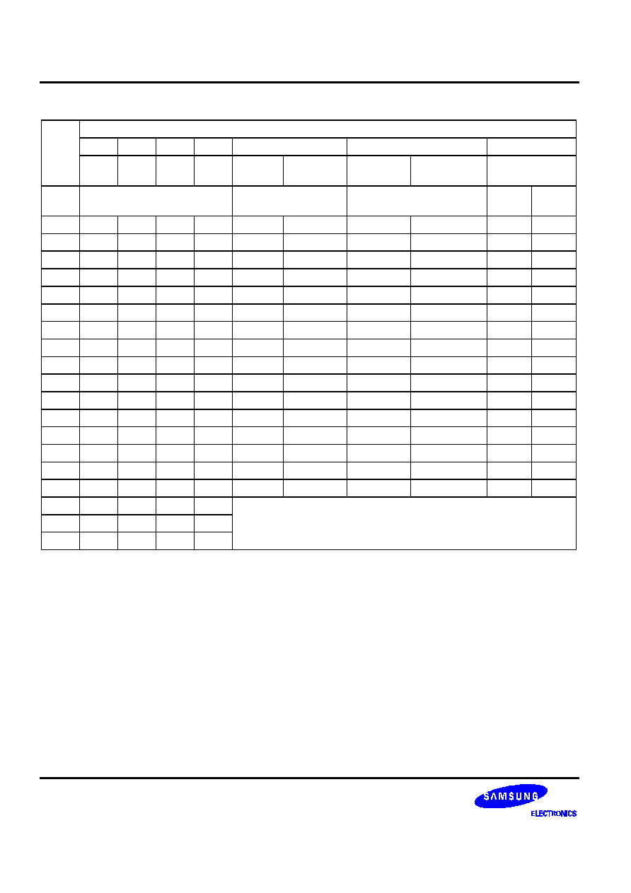
AUTO-SEQUENCE
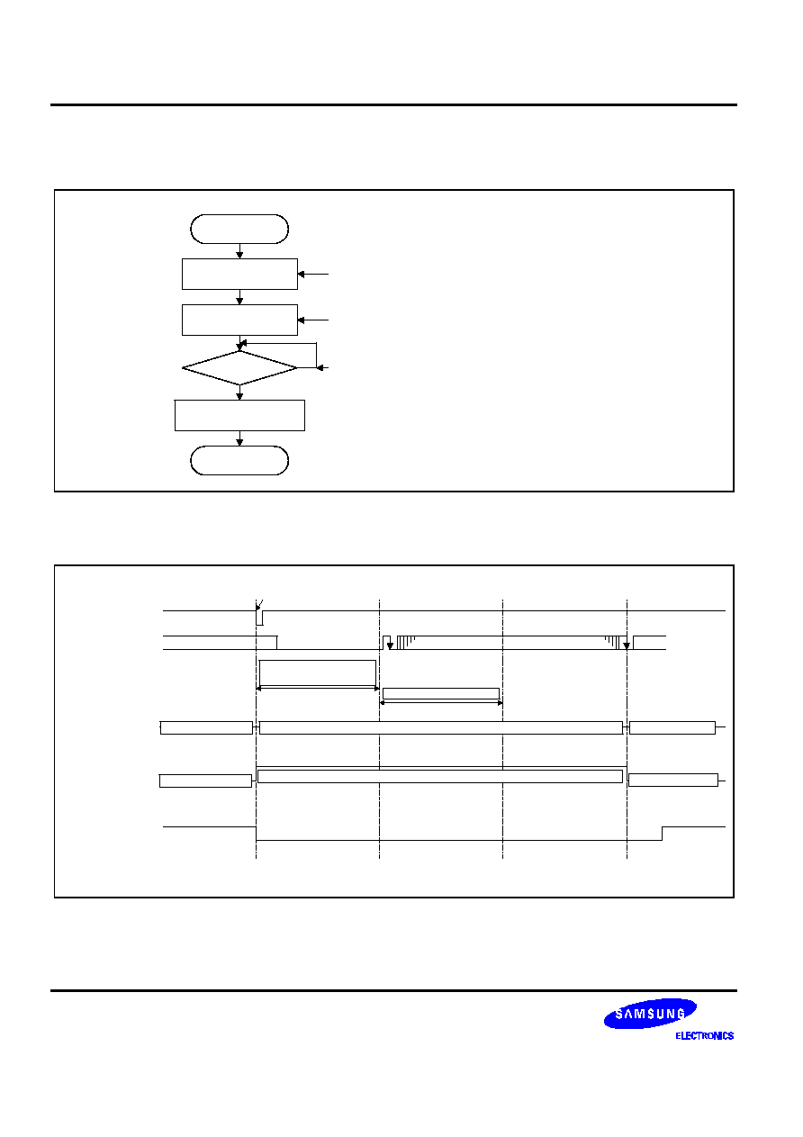
This function executes the chain of commands that execute auto-focus, track jump, and move. MLT latches the
data at time L, and ISTAT is L during auto-sequence. It output H upon.
Auto Focus
Flow-Chart
Focus Search UP
Focus Servo ON
NO
YES
NO
YES
NO
YES
Auto Focus
END
FOK = H
FZC = H
FZC = L
During Blind "E" time set by register 5, FOK and
FZC executions repeat until they become "H".
Timing Chart
Auto-focus receives the auto-focus command from the MICOM in the focus search down state and focus search
up. The SSP becomes focus servo on when FZC changes to L after the internal FOK RZC satisfy 'H', all the time
set blind 'E' (Register $5X). All the internal auto focus executes ended. And this status is sent to micom through
the ISTAT output.
$47 Latch
Blind Time E
FOK, FZC -> H
Search UP
Search DOWN
$02
$03
$03
$03
$08
Internal STATUS
Focus Output
FOK
MLT
Focus Servo ON
FZC
ISTAT
S1L9225X
RF AMP & SERVO SIGNAL PROCESSOR
32
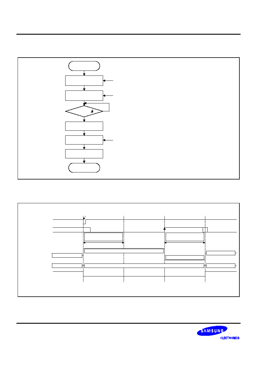
1 Track Jump {$48(FWD), $49(REV)}
Flow-Chart
Track Jump
Sled Servo OFF
WAIT Brake "B"
NO
YES
WAIT (Blind A)
Track REV Jump
Track, Sled Servo On
1 Track Jump
END
Trcnt =
Forward jump when $48 and reverse jump
when $49
Wait using the WDCK reference clock for
blind "A" time, set by register 5.
(1 WDCK = 0.011mS)
Repeat check of whether TRCNT is
continuously in "H" state with the WDCK
reference clock for the brake "B" time, set
by register 5, at the TRCNT rising edge.
1 Track Jump Timing Chart {$48(FWD), $49(REV) inside ( ) Reverse}
$47 ( $49)
Blind Time A
WAIT
Blind Time B
Trcnt "H"
Tracking Farward Jump
Track Servo ON
Tracking Revrese Jump
Track Servo ON
Sled Servo ON
Sled Servo OFF
Sled Servo ON
$25
$28 ($2C)
$28 ($2C)
$2C ($28)
$25
ISTAT
Sled Output
Track Output
TRCNT
MLT
Internal STATUS
Receives $48 ($49) for 1 track jump and sets the blind and brake times through register $5X.
RF AMP & SERVO SIGNAL PROCESSOR
S1L9225X
33
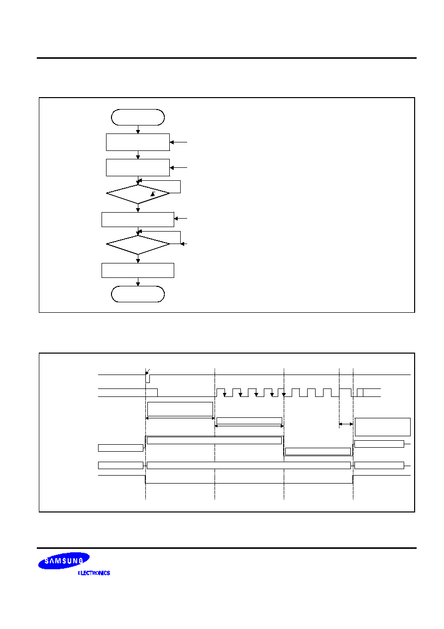
10 Track Jump {$4A(FWD), $4B(REV)}
Flow-Chart
Track FWD Jump
Sled FWD Kick
Trcnt = 5
NO
YES
WAIT (Blind A)
Track REV Jump,
Sled FWD Kick
Track, Sled Servo ON
NO
YES
10 Track Jump
END
C = Over Flow?
Foward jump & kick when $4A and reverse jump &
kick when $4B.
Wait using the WDCK reference clock for blind "A"
time, set by register 5. (1 WDCK = 0.011mS)
Tracking reverse jump & sled forward kick when $4A
and tracking forward jump & reverse kick when &4B.
Repeat check of TRCNT 1's cycle with the WDCK
reference clock to determine if the cycle is long than
the overflow "C" time, set by register 5.
10 Track Jump Timing Chart {$4A(FWD), $4B(REV) inside ( )Reverse }
$4A ( $4B)
Blind Time A
WAIT
Trcnt 5 Count
Tracking Forward Jump
Track Servo ON
Tracking Revrese Jump
Track Servo ON
Sled Servo ON
Sled Forward Kick
Sled Servo ON
$25
$2A ($2F)
$2A ($2F)
$2E ($2B)
$25
ISTAT
Sled Output
Track Output
TRCNT
MLT
Over Flow Time C
Trcnt 1's Time Check
FWD
REV
Internal STATUS
10 track jump executes the tracking forward jump up to trcnt 5track count and turns on the tracking and sled
servos after a tracking reverse jump until trcnt 1's cycle is longer than the overflow 'C' time. This operation
checks whether the actuator speed is sufficient to turn on the servo.

S1L9225X
RF AMP & SERVO SIGNAL PROCESSOR
34
2N Track Jump
Flow-Chart
Track FWD Jump,
Sled FWD Kick
NO
YES
WAIT (Blind A)
Track REV Jump,
Sled FWD Kick
WAIT (Kick "D")
NO
YES
Track Servo ON,
Sled FWD Kick
Tracking & Sled Servo ON
2N Track Jump
END
Trcnt = N?
C = Over
Flow?
Foward jump & kick when $4C and reverse jump &
kick when $4D.
Wait using the WDCK reference clock for blind "A"
time, set by register 5. (1 WDCK = 0.011mS)
Tracking reverse jump & sled forward kick when $4C
and tracking forward jump & reverse kick when $4D.
Repeat check of TRCNT 1's cycle with the WDCK
reference clock to determine if the cycle is longer
than the overflow "C" time, set by register 5.
When $4C, the sled forward kick continues for KICK
"D" time.
When $4D, the sled reverse kick continues for KICK
"D" time.
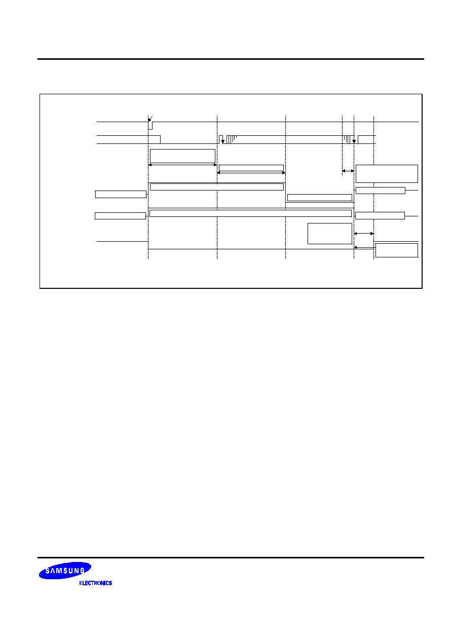
RF AMP & SERVO SIGNAL PROCESSOR
S1L9225X
35
2N Track Jump Timing Chart {$4C(FWD), $4D(REV) inside ( ) Reverse }
$4C ( $4D)
Blind Time A
WAIT
Trcnt N Count
Tracking Forward Jump
Track Servo ON
Tracking Revrese Jump
Track Servo ON
Sled Servo ON
Sled Forward Kick
Sled Servo ON
$25+$17
$2A ($2F)
$2A ($2B)
$2E ($2B)
$25+$18
ISTAT
Sled Output
Track Output
TRCNT
MLT
Over Flow Time C Trcnt
1's Cycle Time Check
FWD
REV
C
C
Kick Time D
Sled FWD Kick
for D Time
Q Data Read
Enable
$26($27)
Internal STATUS
Similar to 10 tracks and executes by adding sled kick by the amount of kick 'D' time and the servo turns on after
lens brake starts.
S1L9225X
RF AMP & SERVO SIGNAL PROCESSOR
36
M Track Jump {$4E(FWD), $4F(REV)}
Flow-Chart
Track Servo OFF,
Sled FWD Kick
NO
YES
WAIT (Blind A)
Tracking & Sled Servo
ON
M Track Jump
END
TRCNT = M?
Sled FWD kick when $4E and REV kick when $4F.
Wait using the WDCK reference clock for blind "A"
time, set by register 5. (1 WDCK = 0.011mS)
Count trcnt with the clock for M amount, set by
register 7.
M Track Jump Timing Chart {$4E(FWD), $4F(REV) inside () Reverse}
$4E ( $4F)
Blind Time A
WAIT
Trcnt N Count
Tracking Servo OFF
Track Servo ON
Treck Servo ON
Sled Servo ON
Sled Forward Kick
Sled Servo ON
$25
$22 ($23)
$22 ($23)
$22 ($23)
$25
ISTAT
Sled Output
Track Output
TRCNT
MLT
FWD
REV
Internal STATUS
Makes Trcnt to clock and counts to the value of M count, set by register 7, to execute sled kick.

RF AMP & SERVO SIGNAL PROCESSOR
S1L9225X
37
Fast Search
Flow-Chart
Track Servo ON,
Sled FWD Kick
WAIT (Blind F)
NO
YES
Track FWD Jump,
Sled FWD Kick
WAIT (Blind K)
Track FWD Jump,
Sled FWD PWM Kick
NO
YES
Track Servo ON,
Sled REV Kick
WAIT (REV. Kick "R")
Tracking & Sled
Servo ON
Fast Search
END
Trcnt = T?
Trcnt = P?
Sled forward kick when $44 and sled reverse
kick when $45.
Tracking forward kick jump and sled forward
kick when $44 and tracking reverse jump and
sled reverse kick when $45
Execute the above conditions until TRCNT is
the same as the brake point "P" count
value, set by register 7.
Repeat checks Trcnt, until Trcnt equals T set by
register 7, like the PD and PW set by register
6, PWMs duty is decided with the PWs PWM1
period width used as the period, and PDs high.
Low duty used as standard 4 bits
(number selected from 0 - 15)
When $44, the sled forward kick continues for
kick "R" time.
When $45, the sled reverse kick continues for
kick "R" time.

S1L9225X
RF AMP & SERVO SIGNAL PROCESSOR
38
Fast Search Timing Chart {$44(FWD), $45(REV) inside () Reverse}
$44 ( $45)
Blind Time F
WAIT
Trcnt P Count
Sled Servo ON
Tracking Forward Jump
Track Servo ON
$25+$17
$26 ($27)
$2A ($2F)
$26 ($27)
$25+$18
ISTAT
Sled Output
Track Output
TRCNT
MLT
FWD
REV
Blind K
WAIT
Trcnt T
Count
Kick "R"
Walt
Sled REV
Kick
Sled Servo ON
Sled Servo ON
Sled Forward Kick
$5XX1 Tracking Servo Mutt
Sled servo
Kick
Internal STATUS
To Note During use of Auto-Sequence
1.
Must send tracking gain up and brake on ($17) during 1, 10, 2N, track jump, and fast search.
2.
Before the auto-sequence mode, MLT becomes 'L' and sequence operation executes at the initial WDCK falling edge
after data latch.
3.
During play, determine as FOK and GFS, not ISTAT.
4.
Tracking gain up, brake, anti-shock and focus gain down are not executed in auto-sequence, and separate command
must be provided.
5.
If the Auto-sequence does not operate as Istat Max time over, apply $40 and use after clearing the SSP internal state.
6.
The above indicated WDCK receives 88.2kHz from DSP. (2x
176kHz)
7.
The auto-sequence internal trcnt and the actual trcnt are slightly different.
8.
Problems can be generated in the algorithm for 2N and M tracks if jump of more than 512 tracks are attempted;
therefore,
use them for less than 512 track jumps, if at all possible.
9.
Use the fast-search algorithm for more than 512 tracks, if possible.
10. When the track is moved by micom, the internal trcnt count setting is created by the $CXXX command, and complete
and
continuous complete signals are output to ISTAT.

RF AMP & SERVO SIGNAL PROCESSOR
S1L9225X
39
TRACKING BALANCE CONTROL CONCEPT
In tracking balance control, the micom compares and monitors the previously set DC voltage window and the
tracking error DC offset, extracted from the external LPF for automatic control.
I/V AMP
FDL FT2
Gain adjust
5bit Arrary
5bit (B4-B0)
from Micom
-
TE1
LPFT
LPF
AND
Logic
D Q
CK
MIRROR
TZC
Trcnt
TBAL
RHO
RLO
E Beam
F Beam
F
E
+
-
+
-
RH
RH
Vdc
5 bit arrary
Gain control
ISTAT2
ISTAT1
Summary of Operation
When the focus and spindle servos are on, tracking balance control turns off the tracking and servo loops to open
the tracking loop, extracts the DC offset by sending the error signal, passed through the optical pick-up and
tracking error amp, through the external LPF, then this offset to the previously set window comparator level, and
then informs of the completion the balance control to the micom through the ISTAT, when the dc offset of the
tracking error amp in window is extracted. At this time, Tracking E beam-side I/V amps gain is selected by
MICOM, and the 5-bit resistance arrays resistance value is selected by the 5-bit control signal.
The values that MICOM applies are 00000
11111. If you select the switch, TESO DC offset increases the
(2.5V-
V)
(2.5V +
V) one step at a time, to enter the pre-selected DC window level. When it enters that level,
the balance adjust is completed, and the switch condition is latched at this time
Because the TESO signal frequency is distributed up to 2kHz, the DC offset that passed through the LPF is not a
correct value, if a DC component exists, and therefore, micom monitors the window output when the TESO signal
frequency is above 1kHz. At this time, the frequency check the Trcnt pin. When TBAL output is H, balance
control is complete.
Vdc < RLI <RHI
RLI < Vdc < RHI
RLI < RHI < Vdc
RHO
H
H
L
RLO
L
H
H
TBAL (AND gate)
L
H
L

S1L9225X
RF AMP & SERVO SIGNAL PROCESSOR
40
RHI: High level threshold value
RLI: Low level threshold value
Vdc: Window comparator input voltage
TBAL: And gate output value of the window comparator output
An Example of Tracking Balance Control
Out of $8000
$801F 32 steps, the upper and lower 32 steps are used. After receiving $8110 as the gain when
the focus and tracking are on, the control flow checks TRCNT frequency to see if the more than 7 TRCNT
entered during 10ms. If yes, it checks the ISTAT, if no, it checks the number of TRCNT three times and goes on
to the ISTAT check.
Repeats fail, it raises the balance switch by 1 step. If ISTAT does not immediately go to H, it for 10 ms during
ISTAT check after which it check whether ISTAT is H continuously for 10ms, is repeated three times. If the three
repeats fail, it raises the balance switch by 1 step.
The above wait 10 ms while running the system. It finds the average of the values obtained the three repeated
execution of the entire above balance control. If only the balance values are from two of the three repeats, these
values are averaged. If only two out of the three tries were successful in getting a balance value, average the
two values. Set as balance switch, this average value +2. This is because the balance for the system and the
minus value for the DC is stable in the system. Precision is important in balance adjust, and about 1+2 sec is
spent as adjust time, which is accounted for.
Balance Control Flowchart 1
Start
- Environment Setting
Focus on $08
Spindle on CLV-S
Tracking off $20
Sled off gain $8110
Balance Window Level
Setting
Check to see if
TRCNT is 7 for 10ms
ISTAT = H?
Present Control Value
+2 Step then, ADJ end.
B0 to B4
Switch Control
Balance ADJ. Start $8000
Other Method
- Can balance adjust while
moving tracks
- $F03 easy to trcnt freq
check in the 2X mode
-10mV - +15mV $84 X0XX
-20mV - +20mV $84 X1XX
Almost
±
20mV
Is ISTAT = H?
Check if ISTAT is H after
waiting 10ms repeat 3 times
Change switch if failure
after 3 repeats
Repeat 3 times
Change switch if failure
after 3 repeats
NO
YES
YES
NO
Balance ADJ. Switch
Incnease by 1 step
$8000 -> $801F
If finds the average of the values obtained the
three repeated execution of the entire above
bacance control.
If only two out of the three tries ware successtial in
getting a bacance value, average the two value.
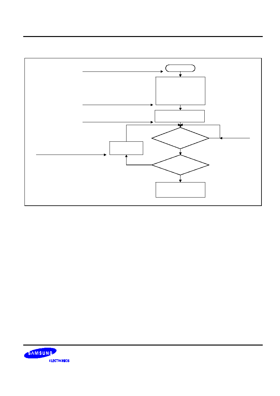
RF AMP & SERVO SIGNAL PROCESSOR
S1L9225X
41
Balance Control Flowchart 2
Start
Environment Setting
- Focus on $08
- Spindle on CLV-S
- Tracking off $20
- Sled off gain $8110
Balance Window Level
Seting
TRCNT Freq is
High Enough?
ISTAT = H?
End ADJ.
B0 to B4
Switch Control
Balance ADJ. Start $8000
Other Method
- Can balance adjust while
moving tracks
- $F03 easy to trcnt freq.
check in the 2X mode
Balance ADJ. Switch
Incnease by 1 step
$8000 -> $801F
-10mV - +15mV $84 X0XX
-20mV - +20mV $84 X1XX
NO
YES
YES
1kHz Check
NO
When Tracking Balance
∑
The balance adjust is from $8000 to $801F, and the switch mode is changed one step at a time by 16-bit data
transmission. After adjustment, a separate latch pulse is not necessary.
∑
If the Trcnt freq. is not high enough, the balance control can be adjusted at $F03 applied 2x mode .
∑
Here, we have suggested tracking off status for the balance adjust, but the same amount of flow can be
balance adjusted while in track move.
∑
Among the 16 bit data, the tracking balance window setting level can be selected from 0: -10 mV
+15mV
1: -20mV
+20mV through the D6 bit.
∑
When the tracking balance adjust is complete, the tracking gain control starts.
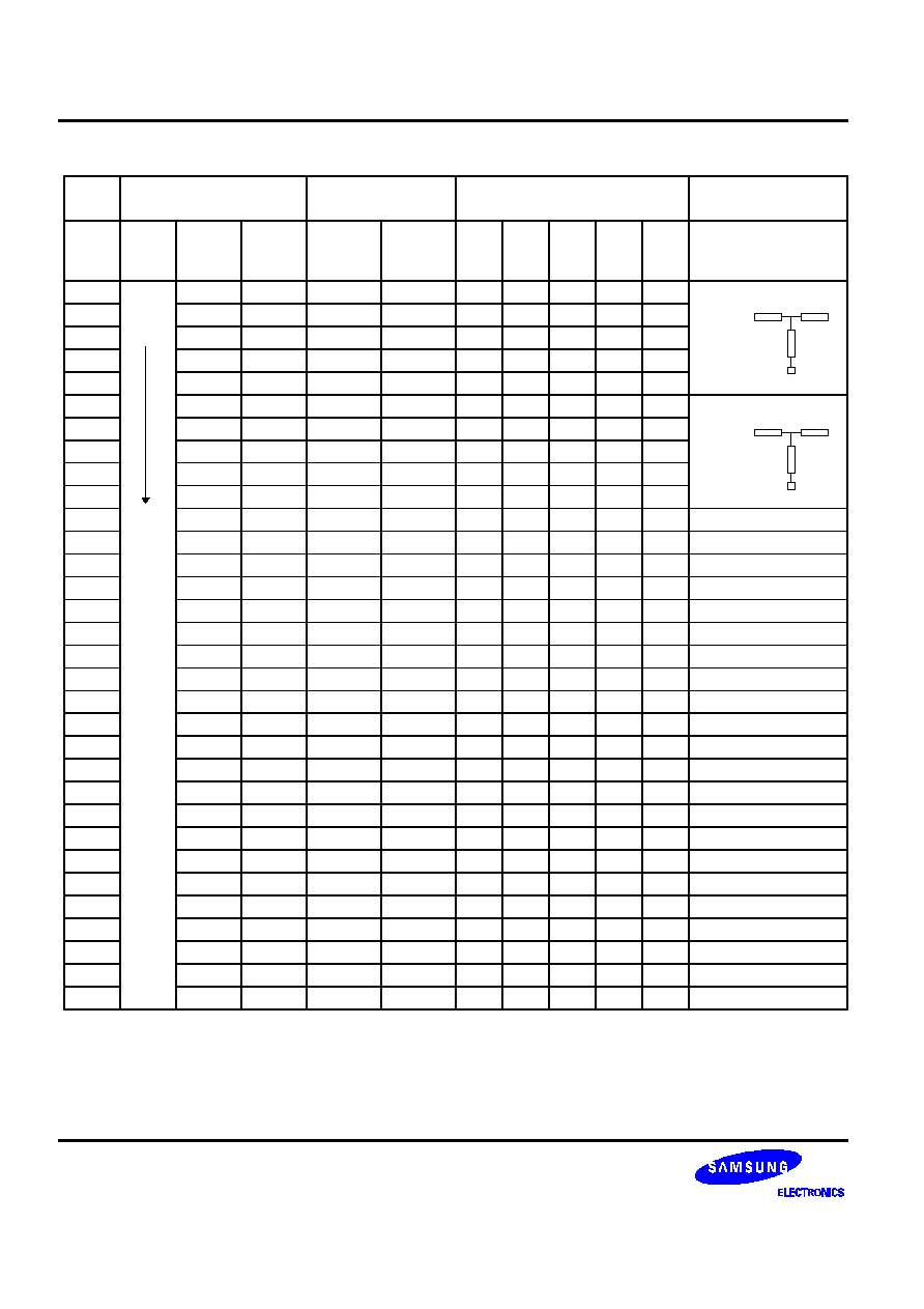
S1L9225X
RF AMP & SERVO SIGNAL PROCESSOR
42
Tracking Balance Equivalent Resistance
Tracking Balance
Fixed Resistance and
Parallel Resistance
Variable Resistance (5bit)
Data
TSIO
offset
F equi-
valent
Res.
E equi-
valent
Res.
100K/
5bit R
5bit
equi-
valence
35K
70K
140K
280K
560K
Comments
$8000
391K
480K
15.22K
17.9K
1
1
1
1
1
$8001
391K
475K
15.6K
18.6K
1
1
1
1
0
$8002
+
391K
468K
16.1K
19.3K
1
1
1
0
1
$8003
391K
463K
16.5K
19.7K
1
1
1
0
0
$8004
391K
455K
17.2K
20.8K
1
1
0
1
1
$8005
391K
451K
17.6K
21.5K
1
1
0
1
0
$8006
391K
444K
18.3K
22.4K
1
1
0
0
1
$8007
391K
439K
18.9K
23.3K
1
1
0
0
0
$8008
391K
433K
19.5K
24.3K
1
0
1
1
1
$8009
391K
426K
20.4K
25.5K
1
0
1
1
0
$800A
-
391K
421K
21.0K
26.6K
1
0
1
0
1
70K//35K = 23.3K 1
$800B
391K
415K
21.9K
28.0K
1
0
1
0
0
280K//140K = 93.3K 2
$800C
391K
409K
22.7K
29.4K
1
0
0
1
1
560K//280K = 186.6K 3
$800D
391K
403K
23.7K
31.1K
1
0
0
1
0
140K//35K = 28K 4
$800E
391K
397K
24.7K
32.9K
1
0
0
0
1
280K//35K = 31.1K 5
$800F
391K
391K
25.9K
35K
1
0
0
0
0
560K//35K = 32.9K 6
$8010
391K
385K
27.1K
37.2K
0
1
1
1
1
140K//70K = 46.6K 7
$8011
391K
380K
28.5K
39.9K
0
1
1
1
0
280K//70K = 56K 8
$8012
391K
374K
30.0K
43.0K
0
1
1
0
1
560K//70K = 62.2K 9
$8013
391K
368K
31.7K
46.6K
0
1
1
0
0
1//2 = 18.56K 10
$8014
391K
361K
33.9K
51.4K
0
1
0
1
1
10//560K = 17.96K
$8015
391K
357K
35.8K
56K
0
1
0
1
0
$8016
391K
350K
38.3K
62.2K
0
1
0
0
1
$8017
391K
344K
41.1K
70K
0
1
0
0
0
$8018
391K
336K
44.5K
80.4K
0
0
1
1
1
$8019
391K
332K
48.4K
93.9K
0
0
1
1
0
$801A
391K
327K
52.8K
112K
0
0
1
0
1
$801B
391K
321K
58.3K
140K
0
0
1
0
0
$801C
391K
315K
65.1K
187K
0
0
0
1
1
$801D
391K
309K
73.6K
280K
0
0
0
1
0
$801E
391K
303K
84.8K
560K
0
0
0
0
1
$801F
391K
298K
100K
0K
0
0
0
0
0
252K
13K
26K
F Equivalence
Resistance
252K
13K
5bit
E Equivalence
Resistance

RF AMP & SERVO SIGNAL PROCESSOR
S1L9225X
43
TRACKING GAIN CONTROL CONCEPT
I/V AMP
I/V AMP
5bit (G4-G0)
From Micom
-
TE1
LPFT
LPF
AND
Logic
ISTAT 2
(Trcnt)
ISTAT 1
TGO
TGH
TGL
E Beam
F Beam
F
E
+
-
+
-
Arrary
Controlled by
5bit Switch
-
TE2
GLI
GHI
Vac
1K, 103
To Micom
Operation Summary
Tracking gain control is executed by comparing the previously set gain set value of the window with the only the
pure AC component of the signal TESO (DC+AC) , which was extracted the resistance divide of the tracking error
amp output, passed through the LPF and DC offset .
The resistance divide regulates the gain by changing the 5 bit resistance combination with micom command. The
tracking gain control is executed under the balance control, the same of focus loop on, spindle servo on, tracking
servo off and sled servo off and controls amount of optical pick-up reflection and tracking error amp gain.
External LPF cut-off freq. Is 1o 10Hz - 100Hz. The window comparator comparison level can be selected
between +150mV - +300mV and +250mV - 200mV using the micom command.
TGL outputs the +150mV and
+250mV comparator outputs to TRCNT.
TGH outputs the +300mV and
+200mV comparator outputs to ISTAT.
Vac < GLI <GHI
GLI < Vac < GHI
GLI < GHI < Vac
TGH (ISTAT output)
H
H
L
TGL (TRCNT output)
L
H
H
Gain control completes control when TGL output is H.

S1L9225X
RF AMP & SERVO SIGNAL PROCESSOR
44
Window Input
TGH (pin19)
TGL (pin18)
GHI
GLI
Vac
1
2
3
Tracking Gain Control
∑
In balance control, 16 bit data transmission changes the switch mode by 1step from $811F
$8100, and ,
after adjustment, a separate latch pulse is not needed.
∑
The H duty check reference of TGL output of Trcnt output is above 0.1ms.
∑
The most appropriate method is chosen among the 4 control modes listed besides the ones above for
control.
∑
Among the 16 bit data, the tracking balance window setting level can be selected from
0: +250mV (TGL) - +200mV (TGH), 1: +150mV (TGL) - +300mV (TGH) through the D7 bit.
∑
When the tracking gain adjust is complete, it enters the tracking & sled servo loop and TOC read.
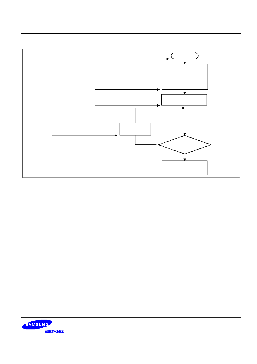
RF AMP & SERVO SIGNAL PROCESSOR
S1L9225X
45
Gain Control Flowchart 1
Start
- Environment Setting
Focus on $08
Spindle on
Tracking off $20
Sled off
Gain Window
Level Setting
Trcnt = H?
End ADJ.
G0 to G4
Switch Control
Gain ADJ. Start $83F
Separate environment setting is
not required when controlling the
gain after controlling balance
+150mV - +300mV $84 1XXX
+250mV - +200mV $84 0XXX
YES
NO
32 TEP reduction of gain
ADJ. Switch from $811F -> $8100
In gain control, the micom command from $811F
$8100 successively executes the down command and goes
status 1 to 2
3. If it reaches status 2, control ends.
∑
Gain Control Method 1
The micom monitors the TGL output of Trcnt and, when it detects the output's H duty (0.1ms), ends. The
window comparator level at this time is +150mV - +300mV.
∑
Gain Control Method 2
The micom monitors the TGO output of Istat and, when it detects the output's H duty (0.1ms), ends. The
window comparator level at this time is +150mV - +300mV.
∑
Gain Control Method 3
The micom monitors the TGL output of Trcnt and, when it detects the output's H duty (0.1ms), ends. It
changes the window comparator level at this time from +150mV - +300mV to +250mV - +200mV. Then it re-
monitors the TGL output of Trcnt, and, if it detects the output's H duty (0.1ms), control ends. If it latches the
middle command between the previous micom command value and latter command value, +200mV gain
control becomes possible.
∑
Gain Control Method 4
The micom monitors the TGL output of Trcnt and, when it detects the output's H duty (0.1ms), it down the
micom command by 1 and control ends. The window comparator level at this time is +150mV - +300mV.
∑
Gain Control Method 5
Gain control is set to 32 steps in total and gain window is set to +250mV.
(That is, start from $811F and head toward $8110) after setting $811F, it monitors the Trcnt to check whether
five Trcnts were detected for 10ms. If yes, control ends, and, if not, it as gain switch is lowered by 1 step.
The above process is repeated three times and the average value obtained from this repetition set as the
gain control switch.
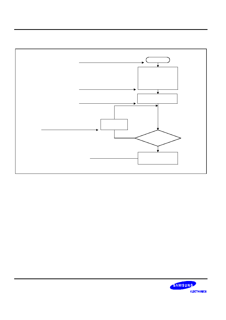
S1L9225X
RF AMP & SERVO SIGNAL PROCESSOR
46
GAIN CONTROL FLOWCHART 2
Start
- Environment Setting
Focus on $08
Spindle on
Tracking off $20
Sled off
Balance Window
Level Setting
Are there 5 Trcnt
for 100ms?
End ADJ.
G0 to G4
Switch Control
Gain ADJ. Start $811F
Separate environment setting is
not required when controlling the
gain after controlling balance
+150mV - +300mV $84 1XXX
+250mV - +200mV $84 0XXX
YES
NO
32 TEP reduction of gain
ADJ. Switch from $811F -> $8110
Gain switch seting after
averaging the 3 repeats

RF AMP & SERVO SIGNAL PROCESSOR
S1L9225X
47
Tracking Gain Equivalent Resistance
Tracking Gain
Data
TERR
Gain
TERR
Gain
5Bit Gain
Ratio
Proportional
Resistance
Combined
Resistance
7.5K
7.5K
3.75K
2.0K
1K
Comments
$811F
0.096
96K/32K
0.032
15.0K
0.5K
1
1
1
1
1
The gain at
$811E
0.272
x 3.0
0.090
15.0K
1.5K
1
1
1
1
0
ratio is
$811D
0.428
0.142
15.0K
2.5K
1
1
1
0
1
calculated in
$811C
0.567
0.189
15.0K
3.5K
1
1
1
0
0
the TSIO
$811B
0.662
0.220
15.0K
4.25K
1
1
0
1
1
terminal.
$811A
0.777
0.259
15.0K
5.25K
1
1
0
1
0
$8119
0.882
0.294
15.0K
6.25K
1
1
0
0
1
$8118
0.977
0.325
15.0K
7.25K
1
1
0
0
0
$8117
1.043
0.347
15.0K
8.0K
1
0
1
1
1
$8116
1.144
0.381
15.0K
9.25K
1
0
1
1
0
$8115
1.200
0.400
15.0K
10.0K
1
0
1
0
1
$8114
1.269
0.423
15.0K
11.0K
1
0
1
0
0
$8113
1.317
0.439
15.0K
11.75K
1
0
0
1
1
$8112
1.378
0.459
15.0K
12.75K
1
0
0
1
0
$8111
1.434
0.478
15.0K
13.75K
1
0
0
0
1
$8110
1.487
0.495
15.0K
14.75K
1
0
0
0
0
$810F
1.548
0.516
7.5K
8.0K
0
1
1
1
1
$810E
1.636
0.545
7.5K
9.0K
0
1
1
1
0
$810D
1.714
0.571
7.5K
10.0K
0
1
1
0
1
$810C
1.783
0.594
7.5K
11.0K
0
1
1
0
0
$810B
1.860
0.620
7.5K
12.25K
0
1
0
1
1
$810A
1.888
0.629
7.5K
12.75K
0
1
0
1
0
$8109
1.941
0.647
7.5K
13.75K
0
1
0
0
1
$8108
1.988
0.662
7.5K
14.75K
0
1
0
0
0
$8107
2.021
0.673
7.5K
15.50K
0
0
1
1
1
$8106
2.0625
0.6875
7.5K
16.50K
0
0
1
1
0
$8105
2.100
0.700
7.5K
17.50K
0
0
1
0
1
$8104
2.134
0.711
7.5K
18.50K
0
0
1
0
0
$8103
2.158
0.719
7.5K
19.25K
0
0
0
1
1
$8102
2.189
0.729
7.5K
20.25K
0
0
0
1
0
$8101
2.217
0.739
7.5K
21.25K
0
0
0
0
1
$8100
2.243
0.747
7.5K
22.25K
0
0
0
0
0

S1L9225X
RF AMP & SERVO SIGNAL PROCESSOR
48
EXAMPLE OF SYSTAM CONTROL
Power ON
Disc Tray Check
Loading
Focus Error Febias Automatic
Control Start
$8780+$87F0+$841 transfer
Replay
Disc Change
Focus Offset Cancel Automatic
Control Start
$08+$867+(200ms wait)+
$86F+$842 transfer
Tracking Offset Cancel Start
$8F1F -> $8F00 (ISTAT->H)
Laser Diode ON
LD ON, P-SUB $8560
Transmission
Limit SW Check
Focusing Auto-Focusing
$47 Transmission
Spindle Servo Loop ON
Tracking & Sled Loop OFF
$20 Transmission
Tracking Balance Adjust
Tracking Gain Adjust
TOC Read
OK?
Disc 8/12Cm Check
Play Back
100ms
ISTAT L -> H?
100ms
ISTAT L -> H?
TIME
100ms Maximum
100ms Maximum
2s Maximum
300ms Maximum
TRY Count
3?
Laser OFF
$85C0 Transmission
Display (no disc)
Standby
Laser OFF
$85C0 Transmission
Display (error),
TRAY Open
Standby
FAIL
NO
YES
PASS
NO
YES
CLOSE
OPEN
Focus OK?
FOK H?
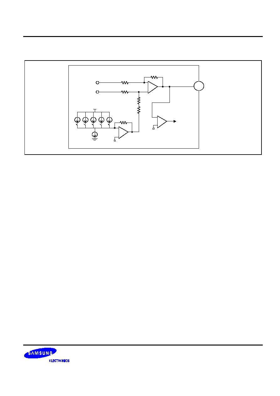
RF AMP & SERVO SIGNAL PROCESSOR
S1L9225X
49
FEBIAS OFFSET CONTROL
X1 X2 X4 X8
3K
+
-
+
-
160K
4K
32K
32K
+
-
fcmpo
164K
vb
va
13
FSEO
vc
Febias offset control starts when it receives the febias offset control start command $841X from the micom.
Febias offset control ends when the focus error amp output above 1/2 VDD after the focus output with 1/2 VDD at
the focus error amp final output terminal. The voltage per 1 step of the focus offset control is approximately
17mV. The 5bit resistance DAC changes from 112mV up to - 112mV in 1 step, after which 1/2 step,
approximately -8mV offset, is applied.
The offset dispersion after febias offset control exists between -8mV - +8mV. The time per 1 step is 5.8ms; for 5
bits and total of 32 steps, the maximum required time is 256ms.
Hardware performs the control from minus offset to plus offset. The febias offset re-control is when 4bit DAC is
reset by $8780. And Reset can be canceled only when the $87F0 applied D2 bit is changed from 0
1. The
Febias DAC latch block reset for electrostatics and system operation is reset by Micom DATA and not by RESET
terminal, the system reset.

S1L9225X
RF AMP & SERVO SIGNAL PROCESSOR
50
FOCUS OFFSET CONTROL
36
+
-
Focus Phase
Compensation
-
+
PS
4
3
0
0
1
1
0
1
0
1
X1
X2
X3
X4
+
-
+
-
+
-
35
08
25
26
12
14
09
3.6K
60K
FZC
I
DFCTI
48K
FS4B
FS3
580K
FGD
FDFCT
FSI
20K
470K
470K
40K
FS2B
82K
40K
10K
50K
5K
FS1
FSET
FLB
FRCH
FEM
FEO
to Digital
VC
Focus Offset control starts when it receives the Focus Offset control start command $842X from micom. Focus
Offset control ends when the focus error amp output below 1.2 VDD after the focus output with 1/2 VDD at the
focus error amp final output terminal. The voltage per 1 step of the focus offset control is approximately 40mV.
The 4 bit resistance DAC changes from 320mV up to -320mV in 1 step, after which 1/2 step, approximately -
20ms offset, is applied. The offset dispersion after Focus offset control exists between -20mV - +20mV. The
Febias Offset can be changed in 10mV step within the micom's
±
100mV range after focus offset control. The
required per 1 step is 5.8ms; for 4 bits and total of 16 steps, the maximum required time is 128ms.
Also, lens-collision-sounds can be generated when adjusting the pick-up with a sensitive focus actuator, so the
Time division that uses 46 ms per step, spending a total of 736 ms, is used. The adjustment is carried out by
Hardware, and it goes from plus offset to minus offset.
For focus offset readjust, 4-bit DAC is reset by $867, and reset can be canceled only when the $86FX applied D2
bit is changed from 0
1. The Febias DAC latch block reset for electrostatics and operation error is reset by
micom DATA and not by RESET terminal, the system reset.

RF AMP & SERVO SIGNAL PROCESSOR
S1L9225X
51
Febias Offset Setting
Febias Control
The FEBIAS offset control is automatically controlled to 0mV and can be controlled to
±
100mV. After the focus
offset automatic control ends after FEBIAS offset automatic control, the command sets the internal positive and
negative offsets in 10mV units to the micom.
RF SUMMING AMPLIFIER APPICATION
The internal switch for the 1x and 2x filter select turns on when it is 1x and off, when 2x. The time constant to fit
the set. The RF 1/V AMP can be controlled to 0.5X 16Step up to 1X - 8X CD-R and CDRW. The information
related to CDR, CDRW disc detector is output as RFO level through the ISTAT. The RFO offset control is
installed to prevent RF level clipping during low RFO voltage and the RFO offset information is output to ISTAT
so that micom can know the RFO information.
+
-
50
49
PDC
PDA
RFM
52
51
PDD
PDB
+
-
+
-
RF Offset
Control
79
RFO
62
61
47K
47K
47K
47K
CDRW Gain Sel
10K
CDRW Gain Sel
IV AMP
10K
RFM2
33pF
33pF
22K
2pF
VC

S1L9225X
RF AMP & SERVO SIGNAL PROCESSOR
52
RF EQUALIZE & AGC
Modulator
3x Gain AMP
HPF
(3dB: 50kHz)
I/V Converter
Control Range
I * 10K
Full Wave Rectifier
(RF Peak Envelope)
Iout = 2gm (Vid/2)
= gm * Vid
= (Iref) * (Vid/Vt)
= Iref * (Vp-Vn)/Vt
if Vn > Vp
Vcagc Increment (tanh (1-X))
if Vn < Vp
Vcagc Decrement (tanh (1+X))
tanh
±
0.1 =
±
0.1
tanh
±
0.5 =
±
0.462
tanh
±
0.1 =
±
0.7
tanh
±
2.0 =
±
0.964
Vref
Vp
Vn
V = I/C (115pF)
EQO-AGC Output
Vin (t)
Vcagc (t)
Vo (t)
+
-
Vin(t) = 0.73x (RFO)
Vo(t) =
R6 (5.5K)
R5 (7.5K)
Vin (t) tanh
(
2Vt
Vcagc(t)
)
The modulator output, which had the Veqc's Tanh term multiplied at the input, passes through the approximately
3X gain terminal to the ARF pad. On the one hand, the output is - rectified as it passes through the HPF having
50kHz pole frequency and follows the peak envelope the RF level. At this time, the pole frequency of the HPF is
set to 50kHz so that the 3T - 11T component can pass through without attenuation. The RF level peak value is
integrated at the 's CAP node after wave rectification. If this peak value is less than the already set voltage
comparison, sinking current is output and, if not, sourcing current is output. The maximum peak value at this time
is 10uA, which is I/V converted and applied as the modulator control voltage. Under the sinking condition, the
Vcagc increases to 1outx10K and multiplied by Tanh (1-X); the sourcing condition, Vcagc decreases to Iout x10K
and multiplied by Tanh (1+X), where X is (Veqc/2Vt).
Overall, after detecting the 3T and 11T levels by full-wave rectification, it is compared to Tanh using the
modulator and multiplied to the gain to realize the wave-form equalize. The above is related to the AGC concept,
which means that a specific RF level is always taken

RF AMP & SERVO SIGNAL PROCESSOR
S1L9225X
53
OTHER BLOCK
Tracking Error Amplifier
The side spot photo diode current input to terminals E and F passes through the E Loop I-V and F Loop I-V
Amps. It is then converted into voltage, in order to gain the difference signal in the Tracking Error Amp. This
portion can perform 0.5X 16 step gain control up to 1X-8X for CD-R and CD-RW. Has the micom programming,
which controls the balance by controlling gain at the E terminal and controls the gain at TEIO.
18
54
53
44
PDE
PDF
TEIO
ISTAT2
+
-
CD-RW, CD
Gain Sel
CD-RW, CD
Gain Sel
46
LPFT2
Win Comp
Win Comp
B_REF_CN
G_REF_CNTR
Gain_UP/D
Gain < 4:
BAL < 4:0 >
16R8R
2R
4R
R
Focus OK circuit
Focus Ok circuit makes the timing window, which turns on the focus in the focus search state by "output" FOK as
L
H if the RF level is above the reference after the difference in DC between and RFO terminals extracted
and compared to the reference DC value.
64
63
EQI
RFO
+
-
+
-
40K
40K
40K
57K
90K
VC + 0.625V
FOKB

S1L9225X
RF AMP & SERVO SIGNAL PROCESSOR
54
MIRROR CIRCUIT
After amplifying the RFI signal, the mirror signal peak and bottom holds.
Peak hold can follow even at defect type
traverse and bottom hold counts the tracks by following RF envelop at a
jump. The mirror output is "L" on the disc track and "H" between tracks. Even if above 1.4 ms is detected, it
outputs "H".
64
EQI
+
-
17K
19K
38K
Peak and
Bottom
Hold
+
-
+
-
+
-
05 MCP
MIRROR
80K
96K
17K
1.5K
EFM Comparator
The EFM Comparator makes the Rf signal into a secondary signal. The Asymmetry generated by a fault during
Disc production cannot be eliminated by only AC coupling, so control the standard voltage of the EFM
Comparator to eliminate it.
02
+
-
40K
EFMI
- RF Double Asymmetry Conection
- EFMI Peak Prevention System
- Asymmetry Hold System
- Asymmetry Gain Control
27 ASY
28
29
EFM2
EFM
x5

RF AMP & SERVO SIGNAL PROCESSOR
S1L9225X
55
Defect Circuit
After RFO signal inversion, bottom hold is carried out using only 2. Except, the bottom hold of holds the
coupling level just before the coupling. Differentiate this with the coupling, then level shift it. Compare the signals
to either direction to generate the defect detect signal.
63
RFO
+
-
37.5K
75K
75K
Bottom
Envelope
+
-
04
DCC2
DEFECT
Bottom
Envelope
06
DCB
03
DCC1
28K
VC
VC+0.6254V
43K
APC Circuit
When the laser diode operates in electrostatic field, the laser output temperature highly negative so the monitor
photo diode controls the laser output at a fixed level. The laser control system is installed to absorb the deviation
of the disc reflection. System controls the laser power using the tracking summing signal of the side beam to a
fixed laser output.
48
PD
47 LD
+
-
+
-
Laser
Control
LDON
5K
5K
55K
0.25K
55K
5K
55K

S1L9225X
RF AMP & SERVO SIGNAL PROCESSOR
56
Center Voltage Generation Circuit
The center voltage is made by using the resistance divide.
+
-
30K
VREF
55
30K
RF Equalize Circuit
The AGC block, which maintains the RF peak to peak level, possess the 3T gain boost. It detects the RF envelop
and compares it to the reference voltage to control the gain.
Receives the RF output to stabilize the RF level to 1Vpeak-peak, which is applied to the EFM slice input.
64
EQI
37
EQC
Equalize
VCA
01
EQO
ATSC
The detection circuit for shock tracking gain up is composed of the window comparator.
42
ATSC
BPF
+
-
+
-
Tracking
Gain UP

RF AMP & SERVO SIGNAL PROCESSOR
S1L9225X
57
Focus Servo
If the focus servo loop phase has been compensated, the focus servo loop mutts if the defect is. The focus error
signal at this time is differentiated by the 0.1uF capacitor to be connected to the terminal and the 470kohms
resistance and is output es through the servo loop. Therefore, the focus output is held to value before the defect
error during defect. The FSET terminal changes the at which the focus loop compensation is at its maximum.
If the resistance to VDDA connected to the terminal, the phase compensation frequency is changed 1.2kHz
below, and GND connected to the terminal, the frequency is changed 1.2kHz above.
During focus search, Fs4 turns on to cutoff the error signal and to output the focus search signal through the
FEO. When the focus is on, FS2 turns on, and the focus error signal input through the FSI is output through the
loop to the output pin.
36
+
-
Focus Phase
Compensation
-
+
PS
4
3
0
0
1
1
0
1
0
1
X1
X2
X3
X4
+
-
+
-
+
-
35
08
25
26
12
14
09
3.6K
60K
FZC
I
DFCTI
48K
FS4B
FS3
580K
FGD
FDFCT
FSI
20K
470K
470K
40K
FS2B
82K
40K
10K
50K
5K
FS1
FSET
FLB
FRCH
FEM
FEO
to Digital
VC

S1L9225X
RF AMP & SERVO SIGNAL PROCESSOR
58
Tracking Servo
The tracking servo phase compensate the tracking servo loop and differentiates the tracking error signal, after
which it outputs the signal through the servo loop. TGU exchanges the tracking gain up/down time constant.
As in the focus loop, the phase compensation peak frequency is varied by the Fset terminal. If the resistance
connected to the FSET terminal changes, the OP Amp dynamic range offeset changes also.
41
09
53
TEIO
FSET
90K
TEO
Tracking
Phase
Compensation
16
TGU
TLPFI
DFCTI
680K
+
-
40 TEM
10K
TM7
68P
F
680K
TG1B
10K
110K
82K
TM1
470K
TG2B
TM4
TM3
The TM7 switch is a brake switch which turns the tracking loop on/off when the actuator is unstable after a jump.
After the servo jumps 10 tracks, the servo circuit leaves the linear range and the actuator sometimes pursues the
unstable track, preventing unnecessary jumps from undesired tracking errors. As the terminal which controls the
tracking servo loop's high frequency gain, the Tgu terminal controls the desired frequency range of the gain
through the external cap.
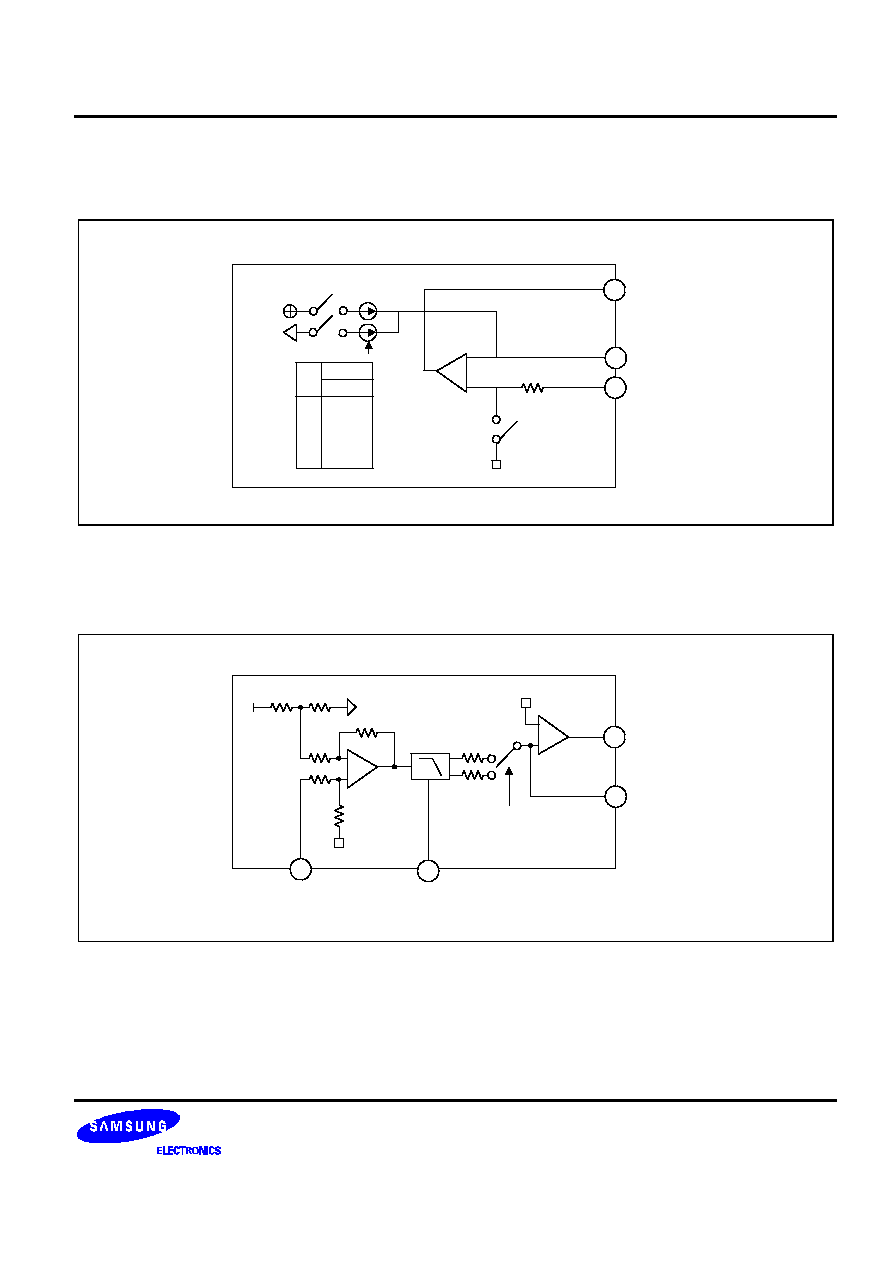
RF AMP & SERVO SIGNAL PROCESSOR
S1L9225X
59
Sled Servo
This servo differentiates the tracking servo and moves the pick-up. It also outputs the sled kick voltage to make a
track jump in the sled axis during track movement.
39
+
-
37 SLM
TM6
TM7
38 SLO
TM2
PS
2
1
0
0
1
1
0
1
0
1
X1
X2
X3
X4
SLP
Spindle Servo & Low Pass Filter
The 200Hz LPF, composed of an external 20kohms resistance and 0.33uF cap, eliminiates the high frequency
carrier component.
+
-
33 SPDLM
34 SPDLO
100K
+
-
09
FSET
25
CLVI
50K
FVCO
Double Speed
220K
22K
22K
220K
220K
220K
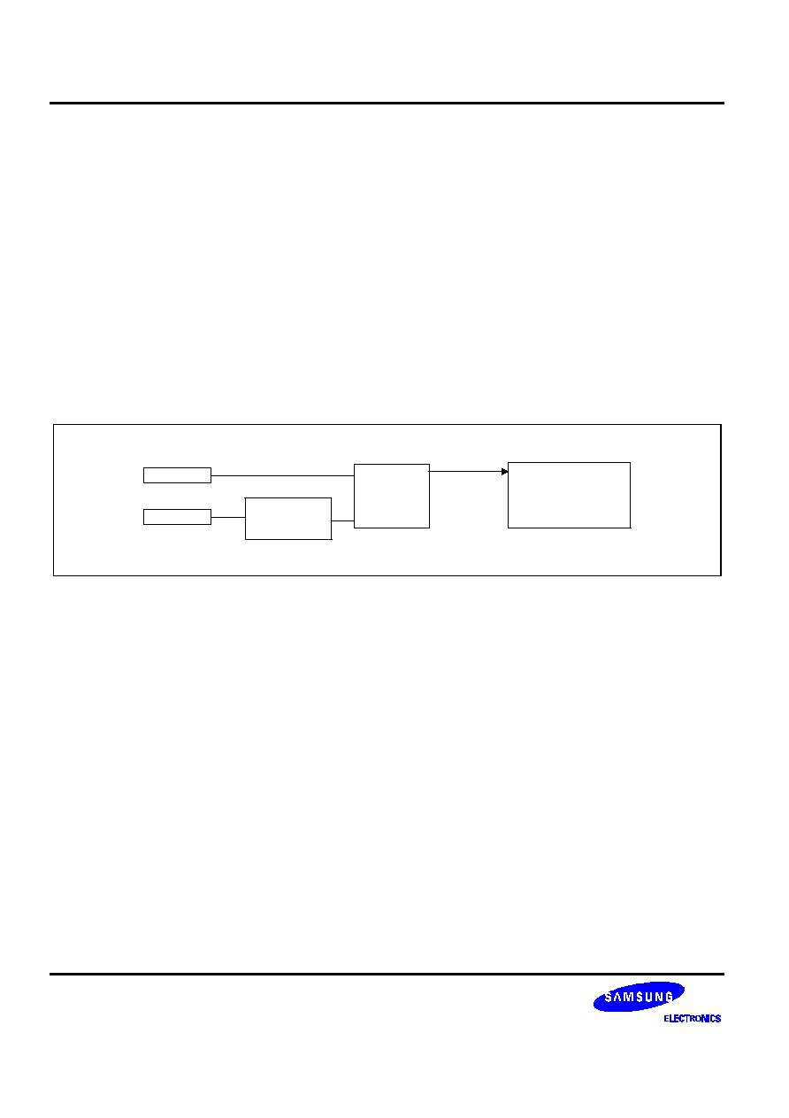
S1L9225X
RF AMP & SERVO SIGNAL PROCESSOR
60
Mirror & Cpeak Mute (use only for tracking mute )
Used against ABEX-725A, this circuit processes the tracking mutting when mirror is detected.
(No recommend) the tracking mutting when EFM duty is above 22T after it is checked.
Mute does not operate in the following four cases.
∑
Micom tracking gain up command transmission (TG1, TG2 = 1)
∑
Anti-shock detection (ATSC)
∑
Lock falls to L
∑
Defect detection
TRCNT Output
TRCNT is output of mirror and TZC.
Mirror is the track movement detection output of the main beam; TZC is the track movement detection output of
the side beam. TRCNT receives these two inputs to determine whether the present pick-up is moving from the
inside to the outside or from the outside to the inside. It is used at $17 tracking brake operation.
MIRROR
TZC
Inverter Delay
TZC EDGE
Detection.
D Q
CK
Trcnt Output
TZC Rising, Falling
EDGE Mirror Output.