 | –≠–ª–µ–∫—Ç—Ä–æ–Ω–Ω—ã–π –∫–æ–º–ø–æ–Ω–µ–Ω—Ç: S1M8653B | –°–∫–∞—á–∞—Ç—å:  PDF PDF  ZIP ZIP |

BASEBAND ANALOG PROCESSOR
S1M8653B
1
INTRODUCTION
The S1M8653B is a baseband analog processing IC for dual-mode CDMA/FM
portable cellular telephones. The S1M8653B interfaces between the analog
RF and digital processing sections of the cellular phone. The receive circuit
functions primarily to translate analog IF signals to the baseband frequency
range and convert analog baseband signals into digital signals. Transmit
circuits convert digital data into analog baseband signals which are then up-
converted to the IF frequency band. The analog inputs and outputs of the
S1M8653B interface with IF transmit/receive circuitry of telephones; the digital
inputs and outputs interface directly with the Mobile Station Modem (MSM).
FEATURES
∑
Dual-mode for CDMA/FM operation
∑
Receive signal path includes:
-- IF to baseband down converter
-- Built-in low pass filter
-- Two 4-bit ADCs
-- Local Oscillator
∑
Transmit signal path includes:
-- Two 8-bit DACs
-- Base-band to IF up converter
-- Local Oscillator
-- Built-in low pass filter
∑
General purpose 8-bit ADC for system monitoring
∑
Power saving modes
∑
Single 3.3V power supply
∑
80 pin LQFP package
∑
S1M8653BQ: CDMA/FM Dual
APPLICATIONS
∑
Dual-mode CDMA/FM cellular telephones
ORDERING INFORMATION
Device
Package
Operating Temperature
S1M8653BQ
80-QFP-1212
-40 to +85
∞
C
80-LQFP-1212
S1M8653B
BASEBAND ANALOG PROCESSOR
2
SYSTEM BLOCK DIAGRAM
RF/IF
System
Baseband
Analog
Processor
Memory &
Peripheral
Mobile Station Modem
CODEC
Figure 1. Dual Mode CDMA/FM Cellular Telephone Block

BASEBAND ANALOG PROCESSOR
S1M8653B
3
BLOCK DIAGRAM
1/4
CDMA
LPF
G
CDMA
4-bit ADC
FM
8-bit ADC
RXIF
RXIFB
2
TCXO
1025
512
1/2
CDMA
4-bit ADC
FM
8-bit ADC
VCO
RXVCO_OUT
RXVCO_T1
RXVCO_T2
FM
LPF
CDMA
LPF
FM
LPF
G
4
FM
LPF
CDMA
LPF
CDMA
LPF
I Q
Div. 2
VCO
Phase
Detector
8-bit
General
Purpose ADC
8-bit
DAC
8
8-bit
DAC
2
2
FM_MOD
TXIF
TXIFB
TXVCO_T1
TXVCO_T2
PD_OUT
PD_ISET
GEN_ADC_IN
4
TCXO/4
RXID3 - 0
RXIFMDATA
CHIPx8
RXQD3 - 0
RXQFMDATA
RXFMCLK
RXFMSTB
IOFFSET
QOFFSET
TXD7 - 0
TXCLK/CLKB
Mode
Control
Logic
SLEEPB
IDLEB
FMB
LOCK
ADC_CLK
ADC_DATA
ADC_EN
Figure 2. Block Diagram

S1M8653B
BASEBAND ANALOG PROCESSOR
4
PIN CONFIGURATION
GND
RXVCO_T1
RXVCO_T2
GND
1
V
DD
RXIF
RXIF
TST
GND
V
DD
FM_MOD
TXVCO_T1
TXVCO_T2
PD_ISET
PD_OUT
GND
TXIF
TXIF
GND
V
DD
V
DD
GND
V
DD
LOCK
GND
TCXO
GNC
GNC
TCXO/4
GNC
VDDP
V
DD
GND
TXDO
RXDQ3
RXDQ2
RXDQ1
RXDQ0
RXDI3
RXDI2
RXDI1
RXDI0
TXCLK
TXD7
TXD6
TXD5
TXD4
TXD3
TXD2
TXD1
GNDD
TXCLK
CHIPx8
V
DDD
RXVCO_OUT
FM IDLE SLEEP
ADCIN
ADCENA
ADCCLK
GND
V
DD
GND
GNC
GNC
RXIFMDATA
RXQFMDATA
RXFMCLK
RXFMSTB
V
DD
IOFFSET
QOFFSET
ADCDATA
GNC
GNC
GNC
GNC
GNC
GNC
S1M8653B
Figure 3. Pin Configuration
BASEBAND ANALOG PROCESSOR
S1M8653B
5
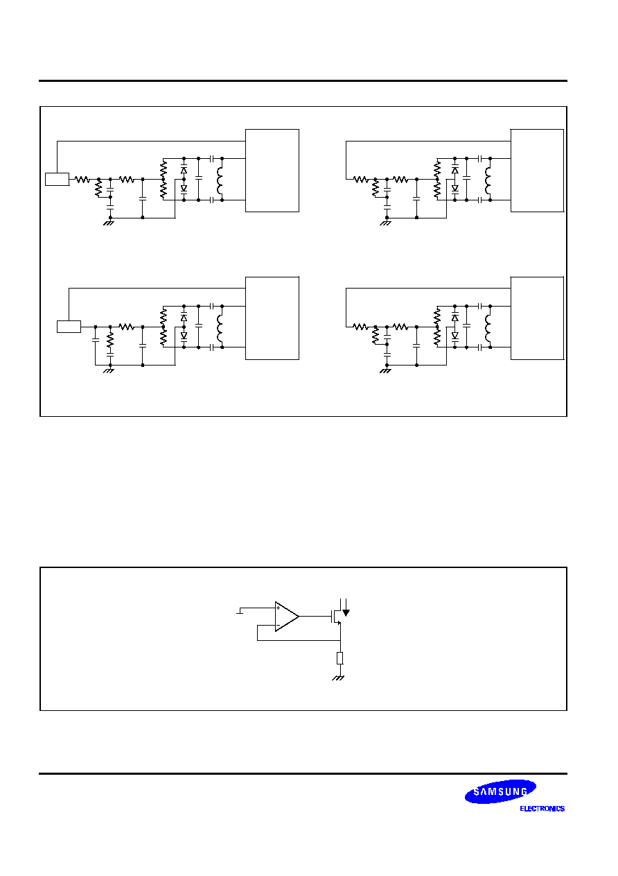
PIN DESCRIPTION
Pin No.
Symbol
Type
Equivalent Circuit
Description
1,4,9,13
GND
P
Analog Ground
2
RXVCO_T1
I
The receive VCO tuning pins connect to an
external LC tank circuit for precise setting
of the receive VCO frequency. The receive
VCO is active in RXTX and IDLE modes for
3
RXVCO_T2
I
CDMA and FM. In SLEEP mode, these
pins are pulled high.
5,10,14
VDD
P
Analog Power (+3.3V).
6
RXIF
I
Analog differential receive IF inputs. These
pins are active in RXTX and IDLE modes
for CDMA and FM. In SLEEP mode, these
pins are pulled low.
7
RXIF
I
8
TST
I
This pin is used during testing. Connect to
analog GND.
11
TXIF
O
Analog differential transmit IF outputs.
These pins are active in CDMA and FM
RXTX modes. In all other modes, these
pins are pulled high.
12
TXIF
O
15
FM_MOD
O
15
Analog FM modulation signal output. It is
active in FM RXTX mode only.
When inactive, it is pulled low.
2
3
6
7
VREF
11
12

S1M8653B
BASEBAND ANALOG PROCESSOR
6
PIN DESCRIPTION (Continued)
Pin No.
Symbol
Type
Equivalent Circuit
Description
16
TXVCO_T1
I
The transmit VCO tuning pins connect to
an external LC tank circuit for precise
setting of the transmit VCO frequency. The
transmit VCO is active in CDMA and FM
RXTX modes.
17
TXVCO_T2
I
In all other modes, these pins are pulled
high.
18
PD_ISET
I
0.64
18
Sets PD_OUT current level.
19
PD_OUT
O
19
Transmit synthesizer phase detector
charge pump output. When inactive, goes
to high impedance state.
20,22,25
GND
P
Analog Ground.
21,23
V
DD
P
Analog Power.
24
LOCK
O
24
Transmit IF synthesizer lock detector
output. Active in CDMA and FM RXTX
modes. LOCK is an open drain, pulled high
by an external pull-up resistor when
inactive.
26
TCXO
I
28
An externally generated 19.68MHz clock
frequency is applied to this pin. It is active
in all modes.
17
16

BASEBAND ANALOG PROCESSOR
S1M8653B
7
PIN DESCRIPTION (Continued)
Pin No.
Symbol
Type
Equivalent Circuit
Description
27, 28
GNC
≠
These pins are used during testing.
Connect to analog GND.
29
TCXO/4
O
29
A clock frequency equal to 1/4 of the TCXO
frequency is output on this pin in all
operating modes.
30,31,32,3
3,34,35,36,
37
GND
P
These pins are used during testing.
Connect to analog GND.
38
V
DD
P
Digital Power.
39
GND
P
Digital GND.
40≠47
TXD0≠TXD7
I
Transmit data input pins for transmit 8-bit
D/A converter TXD7 is the MSB.
48
TXCLK
I
Complementary inputs to transmit D/A
converter.
49
TXCLK
I
50
GND
P
Digital Ground.
51
V
DD
P
Digital Power.
52
CHIPx8
O
52
The CHIPx8 synthesizer is a digital divider
with a ratio of 512/1025 times the TCXO
input frequency. As such, it will have an
average output frequency of 9.8304MHz,
but will not have an exact 50% duty cycle.
When the CHIPx8 synthesizer is disabled
(CDMA SLEEP and FM RX modes) the
CHIPx8 signal is pulled to a logic low.
40
41
42
43
44
45
46
47
48
49
S1M8653B
BASEBAND ANALOG PROCESSOR
8
PIN DESCRIPTION (Continued)
Pin No.
Symbol
Type
Equivalent Circuit
Description
53≠56
RXDI0≠RXDI3
O
CDMA I receive data is output to the MSM
on this 4-bit port. RXDI3 is the MSB.
Active in CDMA RXTX and CDMA IDLE,
otherwise logic low.
57≠60
RXDQ0≠RXDQ3
O
CDMA Q receive data is output to the
MSM on this 4-bit port. RXDQ3 is the
MSB. Active in CDMA RXTX and CDMA
IDLE, otherwise logic low.
61
RXFMSTB
I
Receive FM data strobe. Active in FM
RXTX and FM IDLE modes. Pulled high if
left unconnected.
62
RXFMCLK
I
Receive FM data clock. Active in FM
RXTX and FM IDLE modes. Pulled high if
left unconnected.
63
RXQFMDATA
O
Receive FM Q serial data output. Active in
FM RXTX and FM IDLE modes. High
when inactivated.
64
RXIFMDATA
O
Receive FM I serial data output. Active in
FM RXTX and FM IDLE modes. High
when inactivated.
65, 66
GNC
≠
These pins are used during testing.
Connect to analog ground..
67
GND
P
Analog Ground.
68
V
DD
P
Analog Power.
69
QOFFSET
I
Q channel offset adjust input for CDMA
and RXTX and IDLE modes. The MSM
derives a PDM signal which is filtered by
an external RC at the pin.
70
IOFFSET
I
I channel offset adjust input for CDMA and
RXTX and IDLE modes. The MSM derives
a PDM signal which is filtered by an
external RC at the pin.
53
54
55
56
57
58
59
60
61
62
63
64
69
70
VREF

BASEBAND ANALOG PROCESSOR
S1M8653B
9
PIN DESCRIPTION (Continued)
Pin No.
Symbol
Type
Equivalent Circuit
Description
71
V
DD
P
Analog Power.
72
NC
No connection.
73
ADCCLK
O
General Purpose ADC clock output. When
high, valid data is available on ADCDATA.
Low when inactive.
74
ADCDATA
O
General Purpose ADC serial data output.
Valid data is available when ADCCLK is
high. Low when inactive.
75
ADCENA
I
The General Purpose ADC is enabled and
a conversion is initiated by a positive-
going pulse on this input. Pulled low when
inactive.
76
ADCIN
I
General Purpose A/D analog input. The
voltage applied to this input is digitized by
8-bit general Purpose ADC when ADCENA
is pulsed high.
77
SLEEP
I
CDMA SLEEP mode is invoked when this
pin is low and
FM
is high. Pulled low if left
unconnected.
78
IDLE
I
CDMA IDLE or FM IDLE modes are
invoked when this input is low and SLEEP
is high. Pulled low if left unconnected.
79
FM
I
FM or CDMA mode select. Pulled low if
left unconnected.
80
RXVCO_OUT
O
80
Receive VCO output. Active in CDMA and
FM RXTX and IDLE modes. Pulled low
when inactive.
73
74
75
77
78
79

S1M8653B
BASEBAND ANALOG PROCESSOR
10
FUNCTIONAL DESCRIPTION
The Samsung S1M8653B is an IC that bridges the gap between the analog RF and digital processing sections of
the cellular telephone as shown in Figure 1. The S1M8653B receive signal path translates the acquired IF signal
centered at 85.38 MHz (or 220.38MHz) to base-band where it is then converted to digital data. The digital
baseband signals are sent to the MSM for demodulation. When transmitting, the MSM sends modulated digital
baseband signals to the S1M8653B for up conversion to analog IF signals centered at 130.38MHz.
The MSM handles various digital data according to the CDMA/AMPS standards. It directly interfaces with the
RF/IF sections of the telephone for automatic gain control (AGC) and calibration of the RF signal paths for
receive and transmit. In addition, the MSM performs other miscellaneous digital processing in the CDMA/FM
cellular telephone.
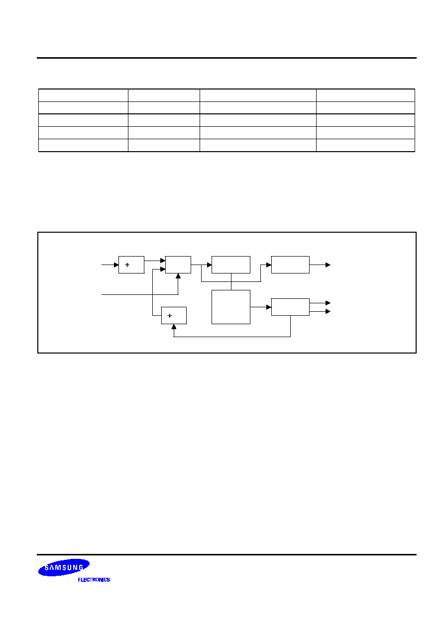
RECEIVE SIGNAL PATH
The S1M8653B receive signal path(see Figure 3) is designed to accept differential IF signals with CDMA spread
spectrum modulation extending
±
630kHz from the IF center frequency of 85.38MHz(or 220.38MHz). The
incoming IF signal is reduced to I and Q base-band components by mixing with 85.38MHz local oscillator (LO)
signals in quadrature followed by low pass filtering.
The 85.38MHz I and Q LO signals are generated on the S1M8653B. The receive VCO is set to 170.76MHz (or
440.76MHz) by an external varactor tuned resonant tank circuit (inductor L and capacitor C connected in
parallel). An external phase lock loop and loop filter network provide the feedback to varactors which tune the
VCO to
170.76MHz. A master-slave divide-by-two circuit generates I and Q signals in precise quadrature for the mixers.
The receive signal path splits into CDMA and FM sections from the mixer output. For CDMA, the base-band
signal extends from 1kHz to 630kHz. Frequency components above 750kHz are out-of-band for CDMA operation.
The mixers and the subsequent CDMA low-pass filters combine to form the down converter which outputs the
CDMA base-band signals. The pass-band, transition band, and rejection band characteristics of these low pass
filters, in conjunction with external IF band-pass filtering, contribute to the ability of the receiver to select the
desired base-band signals from the jamming effects of unwanted signals.
The offset control inputs, IOFFSET and QOFFSET, are used to control the offset at the inputs of the ADCs. The
MSM senses the offset of the digital base-band data and creates a pulse density modulated (PDM) signal for
compensation through long time-constant RC filters. It makes sure that the number of occurrence of symbols,
"1"s and "0"s, in the transmitted data stream is equal. The numbers of the two symbols will differ when DC offset
is introduced in the signal path. The MSM eliminates the unwanted offset by applying appropriate compensating
control signals to IOFFSET and QOFFSET pins.
The down converted base-band analog signal, generated after passing through analog filters, will be sampled at
the falling edges of CHIPx8 clock by two 4 bit flash ADCs, the outputs of which are fed to the MSM as the digital
receive data.
The receive signal path for FM operation is similar to that for CDMA operation. Differences lie in the
characteristics of the I and Q low pass filters and the ADCs. The IF frequency is the same as in CDMA
(85.38MHz or 220.38MHz) but the modulation can only extend
±
15kHz from the IF center frequency, forming a
30kHz wide channel. The low pass filters for FM operation have a much lower bandwidth than those used in
CDMA. The offset of the FM low pass filters is controlled just like the CDMA low-pass filters by the IOFFSET and
QOFFSET input pins.
The lower bandwidth of the FM base-band signal gives rise to the use of very low power 8 bit algorithmic type
ADCs. The FM I and Q analog base-band signals are sampled and held during the analog to digital (A/D)
conversion process. The A/D conversion is initiated with a strobe from the MSM. A serial data stream is output
beginning with the most significant bit(MSB) of the result.
BASEBAND ANALOG PROCESSOR
S1M8653B
11
1/4
CDMA
LPF
4-bit CDMA
ADC
QOFFSET
FM
LPF
4
TCXO/4
RXID[3:0]
IOFFSET
CHIPx8
Synthesizer
TCXO
4-bit CDMA
ADC
CDMA
LPF
FM
LPF
RXIF
RXIF
2
1/2
VCO
RXVCO_T1
RXVCO_T2
FMCLK
RXFMSTB
8-bit FM
ADC
8-bit FM
ADC
4
CHIPx8
RXQD[3:0]
RXIFMDATA
RXQFMDATA
RXVCO_OUT
Figure 3. Receive Section Block Diagram
Transmit Signal Path
The S1M8653B transmit signal path accepts eight bits of I and Q baseband transmit data from the MSM and
outputs modulated IF signal centered at 130.38MHz to the RF transmitter(See Figure 4). The rising edge of the
transmit clock latches incoming data into the I DAC while the falling edge latches data into the Q DAC. The MSM
compensates I and Q data values to account for their half cycle time difference.
Undesirable frequency components are found in the spectrum at the output of the DACs due to output transition
edges and transients, and the transmit clock. To reduce them, each DAC is followed by an anti-aliasing low pass
filter with a bandwidth of 630kHz. Unlike the low pass filters in the receive signal path, these do not require off-set
controls.
The S1M8653B outputs differential IF signals with CDMA spread spectrum modulation extending
±
630kHz from
the transmit IF center frequency of 130.38MHz. The analog I and Q baseband components from the CDMA low-
pass filters are mixed in quadrature with local oscillator(LO) signals at 130.38MHz. The result is summed and
output differentially. The 130.38MHz I and Q LO signals are generated from the transmit VCO running at
260.76MHz. The VCO frequency is set by an external varactor-tuned resonant tank circuit, and the feedback is
provided by an internal phase-lock loop and external loop filter network. A master-slave divide-by-two circuit
generates I and Q signals in precise quadrature for the mixers.
An analog FM modulation signal is constructed from 8-bit digital data supplied by the MSM. Only the Q-channel
DAC is used in the S1M8653B in FM mode, all other CDMA circuits are disabled. The DAC output is filtered by a
low pass anti-aliasing filter and output as the analog FM modulation signal, FM_MOD.
A low speed, 8-bit resolution, successive approximation General Purpose(GP) ADC provides DC measurement
capability to the telephone. It digitizes DC voltages applied to the ADCIN pin from battery level, temperature, and
other low frequency control or monitoring sensors.

S1M8653B
BASEBAND ANALOG PROCESSOR
12
The GP ADC is in a power-down state during normal S1M8653B operation. It is activated by a positive-going
pulse on ADCENA. When this input is driven high, it powers up, samples and holds the voltage applied to ADCIN,
and begins a conversion. The ADC output is available from a serial digital interface. Each of the eight data bits is
valid(MSM first) during the rising edge of the ADCCLK output. When the LSB of the conversion has been clocked
out, the conversion is complete and the ADC returns to a power-down condition. The ADCCLK and ADCDATA
outputs will be low before and after a conversion. Conversions can only be started when the ADC is inactive after
a conversion has been completed. A rising edge of ADCENA during a conversion will be ignored. ADCENA must
be low and a conversion completed before a new conversion can be started.
The S1M8653B has several modes of operation. The CDMA RXTX or FM RXTX modes are in effect when the
telephone is making a call. IDLE mode is in effect when no call is in progress but the telephone receive is active
(ready to answer a call). SLEEP mode is a low-power mode in which the telephone can not receive a call but the
digital processor and keypad are enabled. In Slotted Paging mode, the MSM toggles itself and the S1M8653B
between SLEEP and IDLE modes using a programmable timing interval. This mode allows the telephone to be
contacted by the base station without requiring the telephone to be continuously in IDLE mode. Slotted Paging
mode consumes much less power than IDLE mode.
The states of three digital inputs,
FM
,
IDLE
,
SLEEP
, define the operating modes of the S1M8653B (see Table 1).
These logic signals come directly from the MSM and minimize the power consumed by the S1M8653B by
disabling unused circuits.
8-bit
DAC
TXD[7:0]
TXIF
FM_MOD
TXCLK
2
8-bit
DAC
CDMA
LPF
CDMA
LPF
2
TXIF
Mode
Control
Logic
VCO
FM
LPF
1/2
PLL
Phase
Detector
8-bit General
Purpose ADC
TXCLK
SLEEP
IDLE
FM
TXVCO_T1
TXVCO_T2
TCXO
PD_ISET
ADCENA
ADCIN
PD_OUT
LOCK
ADCDATA
ADCCLK
Figure 4. Transmit Section Block Diagram

BASEBAND ANALOG PROCESSOR
S1M8653B
13
MODES OF OPERATION
Mode
SLEEP
IDLE
FM
Sleep (CDMA)
0
X
X
Idle (CDMA)
1
0
1
RXTX (CDMA)
1
1
1
Idle (FM)
1
0
0
RXTX (FM)
1
1
0
ABSOLUTE MAXIMUM RATINGS
Characteristic
Symbol
Value
Unit
Power supply voltage
V
CC
5.0
V
Voltage applied to inputs
V
A
V
DD
+ 0.5
V
Operating temperature
T
OPR
-40 to +85
∞
C
Storage temperature
T
STG
-55 to +125
∞
C
RECOMMENDED OPERATING CONDITIONS
Characteristic
Symbol
Test Conditions
Min.
Typ
Max.
Units
Power supply voltage
V
CC
3.0
-
3.6
V
Ambient operating temperature
T
a
-40
-
85
∞
C
ELECTRICAL CHARACTERISTICS (V
CC
= 3.3V, T
a
= 25
∞
∞
C)
Characteristic
Symbol
Test Conditions
Min.
Typ
Max.
Units
Power supply current
I
CC1
CDMA RXTX mode
-
35
50
mA
Power supply current
I
CC2
CDMA IDLE mode
-
20
30
mA
Power supply current
I
CC3
CDMA SLEEP mode
-
0.5
1.4
mA
Power supply current
I
CC4
FM RXTX mode
-
25
-
mA
Power supply current
I
CC5
FM IDLE mode
-
13
-
mA
Power supply rejection ratio
PSRR
-
TBD
-
dB
Logic high input voltage
V
IH
V
DD
-0.7
-
-
V
Logic low input voltage
V
IL
-
-
0.3
V
Logic high output voltage
V
OH
V
DD
= 3.0V
2.7
-
-
V
Logic low output voltage
V
OL
V
DD
= 3.6V
-
-
0.4
V

S1M8653B
BASEBAND ANALOG PROCESSOR
14
ELECTRICAL CHARACTERISTICS (Continued) (V
CC
= 3.3V, Ta = 25
∞
∞
C)
Characteristic
Symbol
Test Conditions
Min.
Typ
Max.
Units
Logic input leakage current
I
LC
V
DD
= MAX.
V
IN
= GND to V
DD
-
-
±
100
µ
A
Input capacitance, digital input
C
ID
-
4
-
pF
Digital output load capacitance
C
LD
-
5
-
pF
Digital output load resistance
R
LD
100K
-
-
Input resistance of RX IF input
pins
R
IRXI
RXIF to
RXIF
,
differential
-
500
-
Input capacitance of RX IF input
pins
C
IRXI
RXIF and
RXIF
to
ground
-
4
-
pF
Input impedance of offset adjust
pins
Z
IOFF
IOFFSET, QOFFSET
200K
-
-
Load resistance of TX IF output-
pins
R
LTXI
TXIF to
TXIF
, differential
-
500
-
Load capacitance of TX IF
output pins
C
LTXI
TXIF,
TXIF
to ground
-
4
-
pF
Output impedance of TX IF
output pins
Z
OTXI
TXIF to
TXIF
differential
-
50
-
VCO tuning circuit input
impedance
Z
IVCO
RXVCO_T1,
RXVCO_T2,
TXVCO_T1, TXVCO_T2
-
2K
-
PD_OUT output impedance
Z
OPD
Within compliance range
1M
-
-
LOCK output logic low voltage
V
OLLK
R
LD
10
µ
to V
DD
-
-
0.4
V
LOCK output leakage current
I
LLK
Vout = V
DD
-
-
1
µ
A
TCXO input impedance
ZITCX
-
4K
-
General purpose ADC input
impedance
Z
IGADC
ADCIN
20K
50K
-
General purpose ADC input
signal range
V
SGADC
0.5
-
2.5
V

BASEBAND ANALOG PROCESSOR
S1M8653B
15
SWITCHING CHARACTERISTICS (V
CC
= 3.3V, Ta = 25
∞
∞
C)
Characteristic
Symbol
Test Conditions
Min.
Typ
Max.
Units
TXCLK high time
t
TXCH
CDMA transmit, figure 5
-
50.8
-
ns
TXCLK low time
t
TXCL
CDMA transmit, figure 5
-
50.8
-
ns
TXCLK period
t
TXCY
CDMA transmit, figure 5
-
101.6
-
ns
Data set-up to TXCLK transition
t
SU
CDMA and FM TX,
figure 5, 6
20
-
-
ns
Data hold after TXCLK transition
t
H
CDMA and FM TX,
figure 5, 6
3
-
-
ns
10% to 90% rise time
t
R
CDMA and FM TX,
figure 5, 6
-
-
12
ns
90% to 10% fall time
t
F
CDMA and FM TX,
figure 5, 6
-
-
12
ns
TXCLK to
TXCLK
phase delay
t
PH
CDMA and FM TX,
figure 5, 6
-
-
10
% of
t
F
,
t
R
TXCLK high time
t
TXFCH
FM transmit, figure 6
-
1.39
-
ns
TXCLK low time
t
TXFCL
FM transmit, figure 6
-
1.39
-
ns
TXCLK period
t
TXFCY
FM transmit, figure 6
-
2.78
-
ns
CHIPx8 high time
t
x8H
Figure 7, 10
-
50.8
-
ns
CHIPx8 low time
t
x8L
Figure 7, 10
-
50.8
-
ns
CHIPx8 period
t
x8BCY
Figure 7, 10
-
101.6
-
ns
Digital output delay after CHIPx8
fall
t
DO
Figure 7
-
-
20
ns
10% to 90% rise time
t
x8R
Figure 7
3
-
12
ns
90% to 10% fall time
t
x8F
Figure 7
3
-
12
ns
FMCLK high time
t
FMCKH
FM receive ADC,
figure 8
1
1.39
-
µ
s
FMCLK low time
t
FMCKL
FM receive ADC,
figure 8
1
1.39
-
µ
s
FMCLK period
t
FMCKY
FM receive ADC,
figure 8
-
2.78
-
µ
s
RXFMSTB pulse width high
t
STBPW
FM receive ADC,
figure 8
1
-
-
µ
s
Strobe input valid to FMCLK
falling edge
t
SUS
FM receive ADC,
figure 8
50
-
-
ns

S1M8653B
BASEBAND ANALOG PROCESSOR
16
SWITCHING CHARACTERISTICS (Continued) (V
CC
= 3.3V, Ta = 25
∞
∞
C)
Characteristic
Symbol
Test Conditions
Min.
Typ
Max.
Units
Strobe input valid after
FMCLK falling edge
t
HS
FM receive ADC,
figure 8
50
-
-
ns
10% to 90% rise time
t
FMR
FM receive ADC,
figure 8
-
-
12
ns
90% to 10% falling time
t
FMF
FM receive ADC,
figure 8
-
-
12
ns
Output delay after FMCLK
rising edge
t
DOF
RXQFMDATA,
RXIFMDATA,
FM receive ADC,
figure 8
-
-
50
ns
Enable pulse width high
t
ENPWH
Figure 9
100
-
-
ns
Enable pulse width low
t
ENPWL
Figure 9
100
-
-
ns
ADCENA high to ADCCLK
t
ENCK
Figure 9
-
20
-
µ
s
ADCCLK low
t
GCL
Figure 9
-
1.22
-
µ
s
ADCCLK high
t
GCH
Figure 9
-
1.22
-
µ
s
ADCCLK period
t
GCY
Figure 9
-
2.44
-
µ
s
10% to 90% rise time
t
GR
Figure 9
-
-
12
ns
90% to 10% fall time
t
GF
Figure 9
-
-
12
ns
ADCENA high to conversion end
t
TOC
Figure 9
-
-
40
µ
s
ADCDATA delay after
ADCCLK falling edge
t
GDO
Figure 9
-
20
-
ns
ADCDATA valid before
ADCCLK rising edge
t
GSU
Figure 9
-
1
-
µ
s
TCXO low time
t
XLCL
Figure 10
-
25.4
-
ns
TCXO high time
t
XLCH
Figure 10
-
25.4
-
ns
TCXO period
t
XLCY
Figure 10
-
50.8
-
ns
10% to 90% rise time
t
XLR
Figure 10
-
-
10
ns
90% to 10% fall time
t
XLF
Figure 10
-
-
10
ns
TCXO/4 low time
t
XL4CL
Figure 10
-
50.8
-
ns
TCXO/4 high time
t
XL4CF
Figure 10
-
50.8
-
ns
TCXO/4 period
t
XL4CY
Figure 10
-
101.6
-
ns

BASEBAND ANALOG PROCESSOR
S1M8653B
17
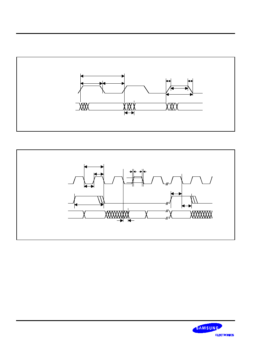
TIMING DIAGRAM
TX-Q
TX-I
TX-Q
TX-I
TX-Q
TX-I
TXD7 - 0
TXCLKB
TXCLK
t
TXCH
t
TXCL
t
TXCY
t
PH
t
R
t
F
t
SU
t
H
Figure 5. CDMA Transmit DAC Timing
TX-DATA
TXD7 - 0
TXCLKB
TXCLK
t
TXFCH
t
TXFCL
t
TXFCY
t
PH
t
R
t
F
t
SU
t
H
TX-DATA
TX-DATA
TX-DATA
Figure 6. FM Transmit DAC Timing
S1M8653B
BASEBAND ANALOG PROCESSOR
18
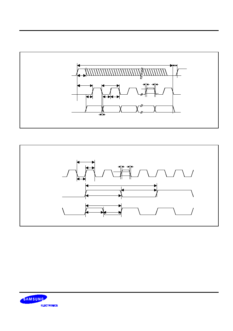
TIMING DIAGRAM (Continued)
RXQD3 - 0
RXID3 - 0
CHIPx8
t
X8H
t
X8L
t
X8CY
t
X8R
t
DO
t
X8F
90%
10%
Figure 7. CDMA Receive ADC Timing
FMCLK
t
FMCKH
t
TXFCY
t
FMCKL
t
FMR
t
FMF
90%
10%
t
SUS
t
HS
Last LSB
MSB
LSB
t
DOF
RXFMSTB
RXQFMDATA
RXIFMDATA
t
STBPW
Figure 8. FM Receive ADC Timing
BASEBAND ANALOG PROCESSOR
S1M8653B
19
TIMING DIAGRAM (Continued)
ADCENA
t
ENPWH
t
TOC
t
ENPWL
t
ENCK
t
GCY
t
GCL
t
GCH
t
GSU
MSB
MSB
10%
90%
t
GR
t
GF
t
GDO
ADCCLK
ADCDATA
Figure 9. General Purpose ADC Timing
TCXO
t
XLH
TCXO/4
CHIPx8
t
XLCY
t
XLL
t
XLR
t
XLF
90%
10%
t
XL4H
t
XL4CY
t
XL4L
t
X8H
t
X8L
t
X8CY
Figure 10. TCXO and CHIPx8 Timing

S1M8653B
BASEBAND ANALOG PROCESSOR
20
SYSTEM PERFORMANCE PARAMETERS
CDMA Rx Performance (V
CC
= 3.3V, Ta = 25
∞
∞
C)
Characteristic
Symbol
Test Conditions
Min.
Typ
Max.
Units
Rx full-path gain
GRX
Overall full path gain
-
38
-
dB
Rx input sensitivity
SENRX
Differential full scale,
input level
-
1.8
-
mVrms
Rx input dynamic range
(Input desense check)
DYNRX
Need two-tone signal
source
Check desense level
-
-
1
dB
Maximum available IF frequency
MAXIF
Check ADC output
240
-
-
MHz
Rx output total harmonic
distortion (ADC linearity check)
THDRX
Check ADC output
-
-
5
%
Offset Adjust gain
GOFF C
IOFFSET, QOFFSET
210
270
330
%
FS/V
Signal path gain variation
GCSCR
with part to part or V
DD
or Temperature
-2
-
2
dB
Signal path out-of-band
frequency attenuation
ATTCR
900kHz
42
60
-
dB
1.2MHz
48
70
-
dB
Overall full-path in-band ripple
FTCR
1kHz to 630kHz
-1.5
0.4
1.5
dB
Rx filter I.Q Gain mismatch
MGIQCR
1kHz to 615kHz
-
0.4
1.5
dB
I.Q Phase mismatch
MPIQCR
Demodulator(Rx Mixer)
Phase mis-match
Measure at I-Q filter
output for 50kHz
-
-
10
degree
FM Rx Performance (V
CC
= 3.3V, Ta = 25
∞
∞
C)
Characteristic
Symbol
Test Conditions
Min.
Typ
Max.
Units
FM receive IF input level
VIFI
sinusoidal, differential
-
2
-
mVrms
FM receive IF single tone
jammer level
VJSF
60kHz,
offset differential
-
300
-
mVpp
Input referred noise
NIRF
I or Q, measured across
FM bandwidth
-
35
45
µ
Vrms
Spurious Content
SCRF
Sum of harmonic and
non-harmonics power
measured at A/D
outputs. Two in-band
tones, each one half of
the maximum input
signal level
-
-44
-40
dBc
BASEBAND ANALOG PROCESSOR
S1M8653B
21
FM Rx Performance (V
CC
= 3.3V, Ta = 25
∞
∞
C)
Characteristic
Symbol
Test Conditions
Min.
Typ
Max.
Units
Spurious content related to
jammer
SCRFJ
Peak in-band spurious
products measured at A/D
outputs. Two-tone Jammer,
50mVrms
@60kHz offset and 6.5mVrms
@122.5kHz offset
+0.733mVrms signal @1kHz
offset
-
-28
-18.4
dBc
Offset Adjust gain
GOFFF
IOFFSET, QOFFSET
210
270
300
%FS/V
Signal path gain variation
GCSFR
With part to part or V
DD
or
Temperature
-
-
±
1.2
dB
Signal path out-of-band
ATTFR
45kHz
48
63
-
dB
frequency attenuation
60kHz
60
70
-
dB
Signal path in-band
frequency flatness
FTCR
0.1kHz to 12.2kHz
-
0.6
1.0
dBpp
Group delay deviation
DGFC
0.1kHz to 12.2kHz
-
-
30
µ
Spp
Residual sideband
suppression
SRFR
28
-
-
dB
CDMA Tx Performance (V
CC
= 3.3V, Ta = 25
∞
∞
C)
Characteristic
Symbol
Test Conditions
Min.
Typ
Max.
Units
IF Output amplitude
VTXCT
Requires full scale quad-
phase signals.
250
300
380
mVpp
Carrier suppression
(Related DC offset)
SCCT
Requires full scale quad-
phase signals.
20
32
dBc
Upper side band suppression
(Related I-Q Phase/gain
mismatch)
USBS
Requires full scale quad-
phase signals.
18
25
dBc
Spurious free dynamic range:
SIFCT
Even harmonics.
20
dBc
IF harmonics
Odd harmonics
9.5
dBc
IF SNR, Noise band 1
SNRCT1
For all frequencies from f
IF
=
±
0.1MHz to f
IF
<
±
2MHz except at IF
harmonics
104
dBc/Hz
Output carrier frequency
CODT
130.38
MHz
In-band filter ripple
FTACT
Measured across the
CDMA bandwidth
1.5
dBpp
Filter total harmonic distortion
THDFLT
4
%
Signal path out-of-band
ATTCR
1.2MHz
-4
dB
frequency attenuation
10MHz
-58
dB

S1M8653B
BASEBAND ANALOG PROCESSOR
22
FM Tx Performance (V
CC
= 3.3V, Ta = 25
∞
∞
C)
Characteristic
Symbol
Test Conditions
Min.
Typ
Max.
Units
IF Output amplitude
VTXFT
Full scale signals.
At nominal V
DD
and room
temperature
-
120
-
mVpp
IF SNR, Noise band 1
SNRFT1
For all frequencies from
f
IF
=
±
0.1kHz to
f
IF
<
±
44MHz.
Exclude frequencies within
±
100kHz f
IF
.
110
-
-
dBc/Hz
IF SNR, Noise band 2
SNRFT2
For all frequencies from
f
IF
=
±
44MHz.
TBD
-
-
dBc/Hz
Output Amplitude variation
VOFT
Part to part, over V
DD
,
temperature
1.6
-
1.6
dB
Spurious free dynamic range:
SIFFT
Even harmonics.
20
12
dBc
IF harmonics
Odd harmonics SFDR is
the ratio in dB of the power
in a 30kHz band around the
harmonics of the f
IF
to the
power in a 30kHz band
around f
IF
.
10
-
-
dBc
FM_MOD output voltage
VFMOD
Full scale. RL>10k
470
550
630
mVpp
FM_MOD amplitude variation
Part to part, over V
DD
,
temperature and aging.
-
-
15
%
FM_MOD spurious free
dynamic range
SFMOD
Two tone inputs, to 120kHz
42
54
-
dB
FM_MOD SNR
SNRFM
Single tone, full scale to
15kHz
87
90
-
dBc/Hz
FM_MOD amplitude flatness
FTAFT
DC to 10kHz
-
0.4
0.6
dBpp

BASEBAND ANALOG PROCESSOR
S1M8653B
23
Receive and Transmit VCO Performance (V
CC
= 3.3V, Ta = 25
∞
∞
C)
Characteristic
Symbol
Test Conditions
Min.
Typ
Max.
Units
TCXO reference input
frequency
FTCXO
-
19.68
-
MHz
TCXO input amplitude
VTCXO
AC coupled
0.5
-
2.0
Vpp
RXVCO_OUT output
frequency range
FRVCO
Depends upon external
components
-
-
500
MHz
RXVCO_OUT phase noise
NPRVCO
Measured at RXVCO_OUT.
The external tank
component have a
minimum Q of 20.
-
-100
-
dBc/Hz
@100
kHz
o.s.
RXVCO_OUT output voltage
swing
VRVCO
AC coupled; measured at
170.76MHz.
-20
-
-
dBm
TXVCO output frequency
range
FTVCO
Depends upon external
components
-
260.76
-
MHz
Lock mode output current
ILOCK
Ris=40KOhms
10
16
20
µ
A
Acquisition mode output
current
IACQ
Ris=40KOhms
128
160
200
µ
A
Maximum IOUT adjustment
range
IMIOUT
Using Ris to vary nominal
output current.
-50
-
+50
%
PD_OUT compliance voltage
VCPD
04
-
V
DD
-
0.4
V
Reference spurious
SREF
-
-
70
dBc
Open loop LO phase noise
(VCO/2)
NLO
CDMA mode, TX IF
outputs, full scale DC
inputs to I and Q. Tank Q >
20
-
-100
-
dBc/Hz
@100
kHz
o.s.
General Purpose ADC Performance (V
CC
= 3.3V, Ta = 25
∞
∞
C)
Characteristic
Symbol
Test Conditions
Min.
Typ
Max.
Units
Offset voltage
GOFF
Mid-scale code referred to
+1.5Volt
-
±
10
-
mV
Gain error
GERR
-
±
2
-
%
DLE
GDLE
-
0.5
1.25
LSB
ILE
GILE
-
0.5
1.25
LSB

S1M8653B
BASEBAND ANALOG PROCESSOR
24
APPLICATION INFORMATION
Receive IF Inputs
The receive IF inputs, RXIF and
RXIF
, differentially drive an input stage within the S1M8653B, where the input
impedance is nominally equal to 500 Ohms. These pins are biased at a DC level of 1.6 Volts and require AC
coupling. AC coupling capacitor values should be chosen to maximize the power transfer from receive IF circuitry
into the S1M8653B. The internal ground and power rails associated with the receive IF input circuitry are pins
4(GND) and 5 (Vcc) respectively.
6
7
500
VREF
1.5V
Figure 11.
Rx
AGC
0 - 300
S1M8653B
* Matching resistors
between AGC and the S1M8653B
Figure 12.

BASEBAND ANALOG PROCESSOR
S1M8653B
25
Transmitting IF Outputs (Use Differential only)
The transmit IF outputs, TXIF and
TXIF
, are differential emitter-follower outputs with nominal output impedance
of 50 ohms. The DC bias on these outputs necessitates AC coupling to the subsequent transmit IF signal path in
order to maximize the power transferred from the S1M8653B. The internal ground and power rails associated
with the transmit IF output circuitry are pins 13(GND) and 14(V
DD
), respectively.
11
12
Figure 13.
TX
AGC
* Impedance transformation network is
recommended between AGC and the S1M8653B
11
12
S1M8653B
Figure 14.

S1M8653B
BASEBAND ANALOG PROCESSOR
26
Rx VCO Output
A single-ended receive VCO signal is output from the RXVCO_OUT(pin 80). The frequency response curve,
shown below, indicates that the output signal levels are about -12dBm in cellular band(170.76 MHz) and -12dBm
in PCS band(440.76 MHz). The IF input sensitivity of typical PLL for the mobile phone applications range from -
25dBm to -30dBm at 450 MHz, well below the receive VCO output levels of the S1M8653B.
The receive VCO circuitry uses two ground pins; one pin is dedicated to the single-ended output drive stage(pin
1) but the other pin(pin 4) is shared by rest of the circuitry. However, a single power pin (pin 5) serves the whole
80
0.15
0.2
0.25
0.3 0.35
0.4
0.45
0.5
-20
(dBm)
-18
-16
-14
(GHz)
VCO Output Level
TX
PLL
Impedance transformation network
S1M8653B
PIN 80
Figure 15. Receive VCO Output Drive Stage
BASEBAND ANALOG PROCESSOR
S1M8653B
27
Rx / Tx Tank Circuit
The frequency of oscillation for any LC resonant tank circuit is determined by, where L and C are the equivalent
inductance and capacitance, respectively, of the tank circuit and parasitics of the S1M8653B. The parasitic
capacitance between the RXVCO_T1 and RXVCO_T2 pins of the S1M8653B has been measured to be about 4
pF. Recommended Q factor of the resonant tank circuit is any value greater than 20.
fo =
1
2
LC
The net capacitance of the tank circuit comprises a varactor diode (Ctr2), a scaling capacitor(Ctr1) connected in
parallel with the varactors, two DC blocking capacitors(Cd) isolating the DC bias of the varactors from the
S1M8653B, and pin-to-pin and pin-to-ground parasitic capacitors (Cpp, Cp). The net tank capacitance is found
from
Ctr2
Ctr2
Ctr1
L
Ps
Cd
Cd
Lp
Lp
Cp
Cp
RL
RL
Figure 16. VCO Tank Circuit Diagram
C =
(Ctr1 + (Ctr2)/2) * 2 + Cd
(Ctr1 + (Ctr2)/2) * Cd
+ Cpp + (Cp)/2
S1M8653B
BASEBAND ANALOG PROCESSOR
28
80
2
3
S1M8653B
100n
47p
47p
1p
1SV229
10k
10k
1n
10k
33n
1.5u
PLL
1k
2k
19
16
17
S1M8653B
27n
120p
120p
4p
10k
10k
1n
10k
47n
2.2u
1.8k
10k
80
2
3
S1M8653B
18n
10p
10p
OPEN
1V229
6.8k
6.8k
15n
10k
4.7k
1.5u
PLL
100p
19
16
17
S1M8653B
27n
68p
68p
5.6p
10k
10k
1n
10k
47n
2.2u
1.8k
10k
VCO Application Circuitry for Cellular Phones
VCO Application Circuitry for PCS Phones
Figure 17. VCO Application Circuitry
PD_OUT Current Setting
The external resistor connected to the PD_ISET determines the level of the charge-pump current sourced by
PD_OUT, which affects the band-width of the transmit PLL.
TCXO (Temperature Compensated Crystal Oscillator)
Shown in the table below is the specifications for this oscillator. It must be temperature compensated, and
provide a stable and accurate 19.68 MHz signal to the S1M8653B.
18 l set
40k
16uA
0.64
Figure 18.
BASEBAND ANALOG PROCESSOR
S1M8653B
29
Table 2. TCXO Requirements
Power supply voltage
3.0V to 3.6V
Frequency deviation
±
0.2ppm
Output level
0.8Vpp min.
Phase noise
-120dBc/Hz@100Hz min.
Nominal frequency
19.68MHz
Frequency control range
235
±
60Hz
Temperature drift
±
2ppm/
∞
C
Control voltage range
+ 0.5V to 2.5V
Power supply sensitivity
±
0.3ppm/V
Control voltage input impedance
100k
min.
Tx PLL Synthesizer
The transmit synthesizer consists of a VCO, a divide-by-two phase splitter, divide by M and N counters, and a
phase detector. The VCO and divide-by-two generate the I and Q LO signals(130.38MHz), which are used in up
converting analog baseband signals to IF signals. The LOCK signal, when asserted logic low, indicates to the
external world, including the MSM, that the transmit PLL is not in lock.
Pin 26
TCXO
19.68MHz
PD
N
LPF
External
Lock
DET
Pin24
LOCK: Io = 10uA
ACQ: Io = 160uA
PDRSET Control
M
M=106
VCO
External
Tuned
Circuitry
1/2 DIV
Quad-P
I
Q
F
VCO
= T
CXO
* M/N
Figure 19. Transmit VCO Synthesizer

S1M8653B
BASEBAND ANALOG PROCESSOR
30
I/Q Offset Control
The full path offset sensitivity has been set to 270% FS/V. Please refer to the functional description section of
this document for more information on the I/Q offset control.
MSM
Voltage
Divider
&
Ripple
Filter
69
70
Vref
Figure 20.
MODEM
69
70
S1M8653B
* Time constant should be longer than 1ms
Figure 21.

BASEBAND ANALOG PROCESSOR
S1M8653B
31
FM Modulation Scaling
The FM_MOD output is used to frequency modulate the transmit VCO. FM_MOD 's voltage swing is normally
550mVpp to achieve the required frequency deviation of the transmit VCO when the device operate in FM mode.
A
±
30kHz deviation of transmit VCO frequency is translated into
±
15kHz deviation of IF frequency by quad-
phase generator (it executes divide-2). A voltage divider can be used as long as the total load on FM_MOD is
greater than 10kOhms.
15
Above 10k
TX
VCO
TX
PLL
Figure 22. FM Modulation Scaling
ADC and DAC Ranges
Since ADCs and DACs on the S1M8653B have access to internally generated references, no external adjustment
or calibrations are required. The GP ADC can be used for various purposes such as monitoring parameters like
battery voltage and temperature. For a nominal power of 3.3 Volts the center of the input voltage range is 1.5
Volts; the input voltage, on the other hand, is equal to 2.0 Volts.
Table 3. ADC Output Coding
Input Voltage
Output Data
Input Voltage
Output Data
FM Receive ADC
General
Purpose ADC
MSB.....LSB
CDMA Receive ADC
MSB......LSB
Greater than positive full-
scale
> 2.500
1111 1111
Greater than positive full-scale
1111
Positive full-scale
2.500
1111 1111
Positive full-scale
1111
99.6% of full-scale
.... ....
50.2% of full-scale
2.492
.... ....
1.504
1111 1110
.... ....
1000 0000
93.7% of full-scale
.... ....
53.3% of full-scale
1110
....
1000
49.8% of full-scale
.... ....
0.4% of full-scale
1.496
.... ....
0.508
0111 1111
.... ....
0000 0001
46.7% of full scale
.... ....
6.7% of full scale
0111
....
0001
Negative full-scale
0.500
0000 0000
Negative full-scale
0000
Less than negative full-scale
< 0.500
0000 0000
Less than negative full-scale
0000
S1M8653B
BASEBAND ANALOG PROCESSOR
32
Transmit DAC
The two 8-bit transmit DACs contained in the S1M8653B transform digital data from the MSM into analog signals.
Each data conversion is made on the rising edge of TCLK and TCLKB signals and output to an internal anti-alias-
ing filter. The transmit DAC has been implemented using the current segmentation method.
Table 4. Transmit DAC Performance
Characteristics
Values
Test Conditions
DLE
±
1
There Could Be Missing 1 Code
ILE
±
1.25
Temperature Code Drift
±
2
Codes -30 to + 80
∞
C
Power Supply Code Drift
±
1
Code V
DD
= 3.0V to 3.6V
Power Setup Time
A proper operation during the initial power on stage requires reset-ting of internal digital circuits. The reset signal
used for this purpose is derived from the rising edge of V
DD
as it rises up to the full power level. For a proper
operation of the S1M8653B, the rise time (Tset) of V
DD
must be less than 700
µ
S.
TEST
V
CC
/V
DD
Figure 23.
BASEBAND ANALOG PROCESSOR
S1M8653B
33
TEST CIRCUIT
1
S1M8653B
2
3
4
5
6
7
8
9
10
11
12
13
14
15
16
17
18
19
20
21
22
23
24
25
26
27
28
29
30
31
32
33
34
35
36
37
38
39
40
60
59
58
57
56
55
54
53
52
51
50
49
48
47
46
45
44
43
42
41
80
79
78
77
76
75
74
73
72
71
70
69
68
67
66
65
64
63
62
61
10k
V
DD
=3.3V
Digital GND
V
C
C=3.3V
Analog GND
FID
FQD
FCLK
FSTB
0.01u
1n
1n
0.01u
1n
1n
0.01u
sw1-1
Spectrum
Analyzer
Volt
Meter
Logic
Analyzer
TD1
TD2
TD3
TD4
TD5
TD6
TD7
TCUK
Pattern
Generator
TCUKB
ID0
ID1
ID2
ID3
QD0
QD1
QD2
QD3
4-bit
DAC
4-bit
DAC
Logic
Analyzer
Spectrum
Analyzer
Spectrum
Analyzer
8-bit serial-> parallel
8-bit DAC
Spectrum
Analyzer
Spectrum
Analyzer
8-bit serial-> parallel
8-bit DAC
Pattern
Generator
FM
IDLE
SLEEP
GENA
GD
GCLK
Logic
Analyzer
8-bit serial-> parallel
8-bit DAC
GD
GENA
Spectrum
Analyzer
GCLK
Pattern
Generator
Pattern
Generator
FM
IDLE
SLEEP
500
100p
5p
TPVCO
a
b
100p
50
a
b sw1-1
100p
RxVCO
170.76MHz
sw4-1
sw4-2
sw4-3
SPRIF
RXIF3
RXIF2
RXIF1
T1
TTXIF
sw2-1
a
b
50
sw3
b
a
0.01u
sw2-2
TxVCO
100p
4p
100p
1SV229
10k
10k
1n
2.2u
47n
10k
1.8k
10k
a
b
0.01u
TLOCK
VCLK
f=19.68M
Mag=0.5V
sinewave
TLOCK1
* Power on transient time must be width 10ms
0.01u
0.01u
TCHIPx8
TCIADO
1k
150p
TCQADO
1k
150p
1k
0.01u
TFQADO
1k
0.01u
TFIADO
FMSTB
1k
0.01u
TGADO
FMCLK
3.3V
0.01u
ROOFS
RIOFS
RGADC
Figure 24. Test Circuit

S1M8653B
BASEBAND ANALOG PROCESSOR
34
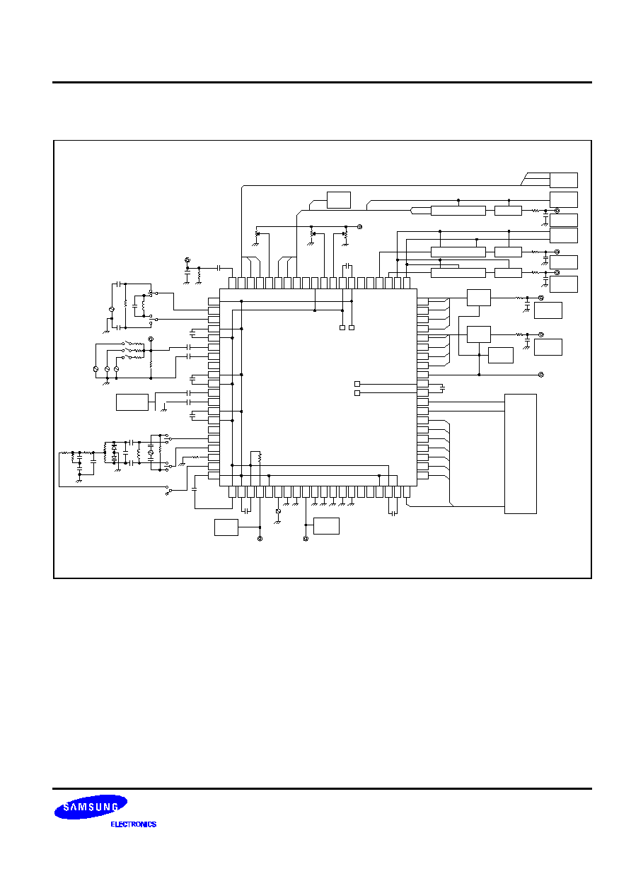
APPLICATION CIRCUIT
1
S1M8653B
2
3
4
5
6
7
8
9
10
11
12
13
14
15
16
17
18
19
20
21
22
23
24
25
26
27
28
29
30
31
32
33
34
35
36
37
38
39
40
60
59
58
57
56
55
54
53
52
51
50
49
48
47
46
45
44
43
42
41
80
79
78
77
76
75
74
73
72
71
70
69
68
67
66
65
64
63
62
61
V
DD
=3.3V
Digital GND
V
C
C=3.3V
Analog GND
0.01u
1n
1n
0.01u
1n
1n
0.01u
TCXO
OSC
0.01u
0.01u
* Power on transient time must be width 10ms
0.01u
0.01u
0.01u
PLL
Rx IF
AGC
Tx IF
AGC
40k
0.1u
0.1u
Analog
Switch
SYNTH_LOCK
TCXO/4
TX_IQDATA0 - 7
TX_CLK
TX_CLK/
CHIPx8
C_RX_IDATA0 - 3
C_RX_QDATA0 - 3
FM_RX_IDATA
FM_RX_QDATA
FM_RX_STB
FM_RX_CLK
ADC_ENABLE
ADC_DATA
ADC_CLK
I_OFFSET
Q_OFFSET
10k
10k
ANALOG SWITCH
MODE CONTROL
47p
100n
47p
1p
1SV229RV
10k
10k
1n
10k
33n
1.5u
2k
1k
27n
120p
120p
4p
10k
10k
10k
10k
1.8k
4.7n
2.2u
10k
Figure 25. Application Circuit
BASEBAND ANALOG PROCESSOR
S1M8653B
35
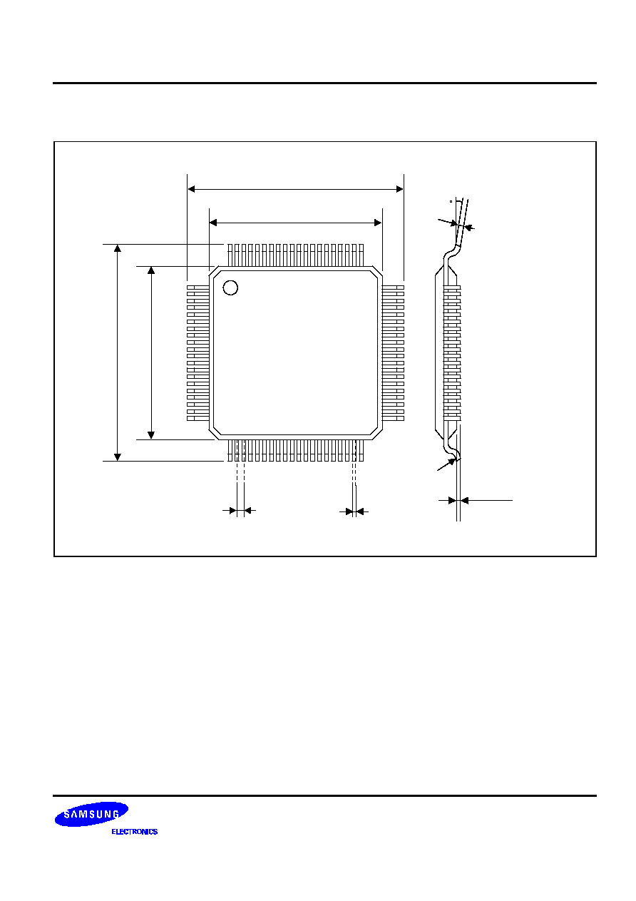
PACKAGE DIMENSION
12.00 (0.471) Normal
14.00(0.551) Normal
12.00 (0.471) Normal
14.00 (0.551471) Normal
0.15
0-10
0.55 (0.022) Max.
0.20 (0.006) Max.
0.45 (0.018) Min.
0.27 (0.014) Max.
0.09 (0.010) Min..
1.60 (0.057) Max.
0.09 (0.002) Min.

S1M8653B
BASEBAND ANALOG PROCESSOR
36
NOTES