RX IF/BBA WITH AGC
S1M8656A
1
INTRODUCTION
S1M8656A/8657 are CDMA/AMPS Dual Mode IF/ baseband IC which is
divided into three main parts - IF frequency processing, basband
processing , and digital interface. The receiver IC (S1M8656A)and
transmitter IC (S1M8657) are provided as a KIT.
S1M8656A is a receiver IC, installed with a Rx AGC, Baseband
Converter, Baseband analog filter, and A-D Converter. It can send a
digital baseband signal to the digital baseband IC. The S1M8657X01 is a
transmission-only IC, installed with a Tx AGC, IF frequency converter,
analog filter, D-A Converter, PLL, 8-bit A-D Converter for the system
monitor, and 3-input analog switch. It connects the digital baseband IC to
the RF processing. Designed to operate in direction connection with the
MSM, S1M8656A and S1M8657 are fabricated on the Samsung's 0.5um
high-speed, high-frequency BICMOS processing and can achieve
superior high frequency and low power digital operations.
Its operating voltage is 2.7V ≠ 3.6V, and operating temperature
-30
∞
C ≠ +85
∞
C .
FEATURES
∑
CDMA/AMPS Dual Mode
∑
AGC input signal range : 90dB
∑
QPSK Baseband Converter
∑
Built-in I ,Q Baseband signal extractor LPF
∑
Built-in 4-bit ADC for converting I and Q CDMA analog baseband signals to digital baseband signals
∑
Built-in 8-bit ADC for converting I and Q FM analog baseband signals to digital baseband signals
∑
Adopts the Rx SLOT function to minimize the AMPS Mode consumption power
∑
Built-in VCO for baseband conversion
∑
Built-in Modem PDM control circuit to compensate the I and Q offsets
∑
3-Line Serial Port Interface (SPI)
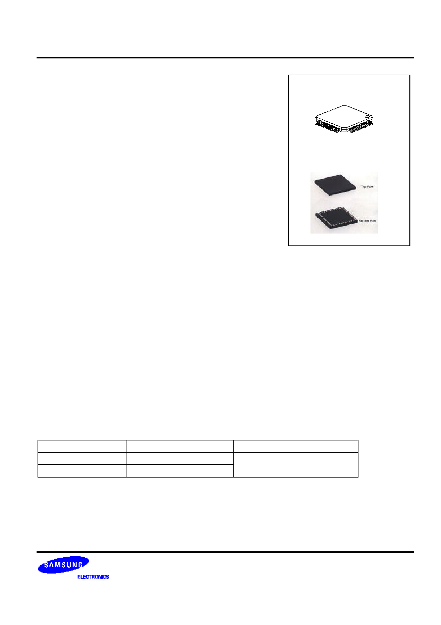
ORDERING INFORMATION
Device
Package
Operating Temperature
+ S1M8656A01-E0T0
48-LQFP-0707
-30 to +85
∞
C
+ S1M8656A01-F0T0
48-BCC-7.0
◊
7.0
+ : New product
48-BCC-7.0
◊
7.0
48-LQFP-0707
S1M8656A
RX IF/BBA WITH AGC
2
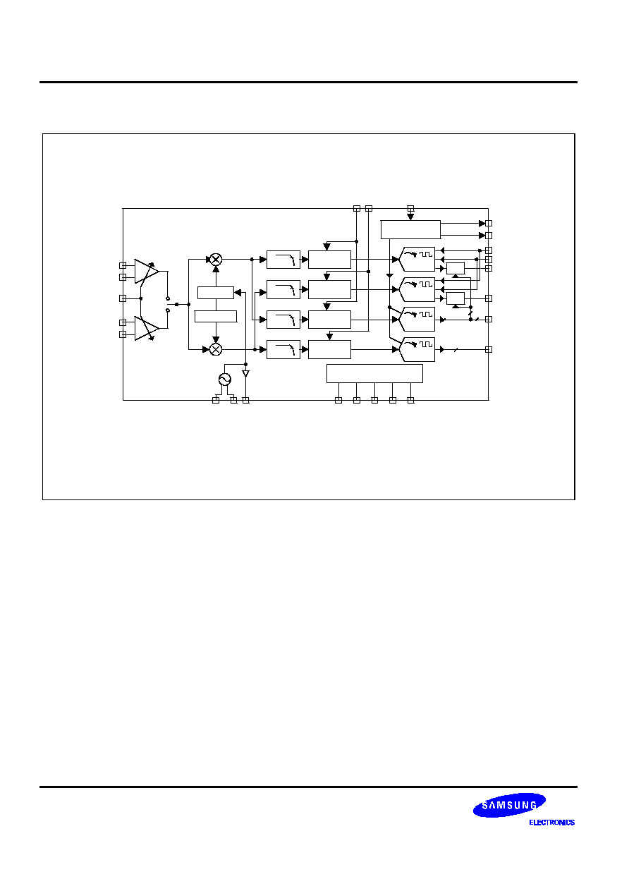
BLOCK DIAGRAM
CRX_IF1
TCXO/N
CHIPx8
FMCLK
FMSTB
FMRID/RXID1
RXID2-3
RXQD0-3
CRX_IF2
RAGC_CONT
FRX_IF1
FRX_IF2
RXVCO_T1
RXVCO_T2
RXVCO_OUT
FMB/DATA
IDLEB/STB
SLEEPB/CLK
SLOTB
SEN
I_OFS
Q_OFS
TCXO
FMRQD/RXID0
1/2Div.
90D-PSN
LPF
LPF
LPF
LPF
OFFSET
CONTROL
OFFSET
CONTROL
OFFSET
CONTROL
OFFSET
CONTROL
3-line Serial Port Interface
MODE Control
DIV.N/CHIPx8
ADC
ADC
ADC
ADC
SW
SW
2
2
4
4

RX IF/BBA WITH AGC
S1M8656A
3
PIN CONFIGURATION
FMCLK
GND
VCC
GND
VCC
RAGC_CONT
GND
FRX_IF1
FRX_IF2
CRX_IF1
CRX_IF2
FMSTB
GND
VCC
VCC
GND
VCC
N.C
GND
VCC
RXVCO_T1
RXVCO_T2
GND
VCC
SEN
Q_OFS
I_OFS
SLOTB
IDLEB/STB
FMB/DATA
SLEEPB/CLK
N.C
GND
VCC
TCXO
TCXO/N
CHIPx8
RXQD3
RXQD2
RXQD1
RXQD0
GND
RXID3
RXID2
FMRID/RXID1
FMRQD/RXID0
VDD
RXVCO_OUT
1
2
3
4
5
6
7
8
9
10
11
12
13
14
15
16
17
18
19
20
21
22
23
24
48
47
46
45
44
43
42
41
40
39
38
37
36
35
34
33
32
31
30
29
28
27
26
25
S1M8656A
S1M8656A
RX IF/BBA WITH AGC
4
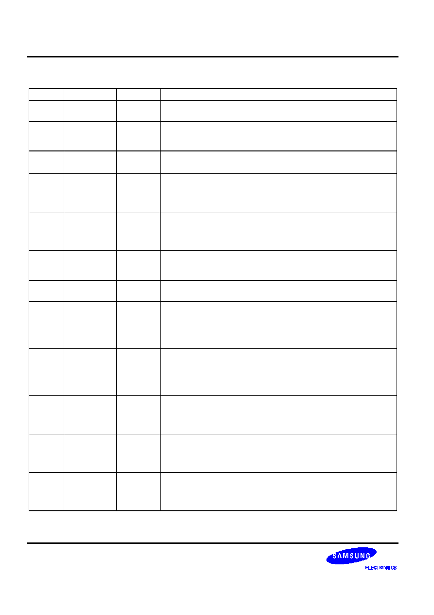
PIN DESCRIPTION
Pin No
Symbol
I/O
Description
1
FMCLK
SEN
FM ADC clock input ,received from the modem.
Signal frequency is 360kHz; if unconnected, it becomes LOW.
2
FMSTB
DI
FM STROBE input. Signal that controls the FM ADC initialization and
A-D conversion start. CLOCK frequency is 40kHz, which is received
from the MODEM; if unconnected, it remains at LOW.
7
RAGC_CONT
AI
AGC gain control input. The input voltage is allowed up to V
DD
.
It remains at High impedance during SLEEP.
9
10
FRX_IF1
FRX_IF2
AI
FM IF input terminals, which have an input impedance of about 865
;
generally, the FM IF SAW filter is connected to them. Usually, the IF
SAW output is single-ended.
When these terminals are not used, they remain at High impedance.
11
12
CRX_IF1
CRX_IF2
AI
CDMA IF input terminals, which have an input impedance of about
865
; generally, the CDMA IF SAW filter is connected to them.
Usually, the IF SAW output is differential. When these terminals are
not used, they remain at High impedance.
21
22
RXVCO_T1
RXVCO_T2
AI
Very sensitive terminal, which is connected to the oscillation L-C
resonance circuit.
Their impedance are about 2k
25
RXVCO_OUT
AO
Output for the PLL, able to output about -12dBm.
When this is not used, it remains at high impedance.
26
SEN
D
Input that permits/not permits SPI BUS control.
If the input is high, SPI control is allowed, and its related 3-pins, STB,
DATA, and CLK, perform their functions; if Low, related 3-pins,
IDLEB, FMB, and SLEEPB, are allowed to perform parallel control.
When this is not used, it remains at Low.
27
28
Q_OFS
I_OFS
AI
Control DC input for removing the DC offset generated in the BBA
and system during CDMA and AMPS Mode. The control DC is
generated in the modem in PDM form, passes through the R-C filter
and is converted to DC, which is sent to this input terminal. No pull
up/down should be performed at this terminal.
29
SLOTB
DI
This pin becomes Low during CDMA SLEEP Mode or FM RX Mode,
the system is assumed to be in the Rx SLOT mode, and all functions
are stopped except for the VCO, VCO buffer and TCXO/N. No
external clock inputs are not required in this product with this function.
30
IDLEB/STB
DI
When SEN is high, this pin becomes the STROBE input with the
permit of the 3-LINE Serial control input.
When SEN is low, parallel control input is allowed and this pin
executes the IDLEB function. If this pin is opened, it remains at Low.
31
FMB/DATA
BI
When SEN is high, this pin inputs and outputs data with the permit of
the 3-line serial control input. When SEN is low, parallel control input
is allowed and this pin performs IDLEB. If this pin is opened, it
remains at Low.

RX IF/BBA WITH AGC
S1M8656A
5
PIN DESCRIPTION (Continued)
Pin No
Symbol
I/O
Description
32
SLEEPB/CLK
DI
When SEN is high, this pin inputs the clock with the permit of the 3-
line serial control input. When SEN is low, parallel control input is
allowed and this pin performs SLEEPB. If this pin is opened, it
remains at Low.
36
TCXO
AI
Reference frequency input terminal connected to the VCTCXO output.
When this pin stops, only DC bias is delivered to maintain the DC
charge value of the capacitor connected externally.
37
TCXO/N
DO
Division output of the TCXO Reference frequency input. 3-different
division ratio and 2- output drive capacities can be selected through
the SPI bus control. Default : 4.92MHz, Weak OUT *division ratio : 1,
1/4, 1/16
38
CHIPx8
BI
CHIPx8 CLOCK output terminal. It has a division ratio of 512/1025 for
the TCXO reference frequency.
Therefore, it cannot have a perfect 50% duty. When this terminal is
not used (CDMA SLEEP, FM IDLE), it remains at Low. This pin can
be used exclusively for the externally generated CHIPx8 CLOCK input
using the SPI BUS control.
39
40
41
42
45
46
47
48
RXQD3
RXQD2
RXQD1
RXQD0
RXID3
RXID2
RXID1/FMRID
RXID0/FMRQD
DO
CDMA A-D Converter's digital outputs, which are connected to the
modem data input pins. These data are synchronized at CHIPx8's
rising edge and output. Because they are valid at the falling edge, the
data are latched at the falling edge in the modem.
Because the number of 48-pins are restricted in this product, pins 47
and 48 are shared with the FMDATA pin.
4, 6,
14,
15, 17,
20, 24
VCC
AI
Power input terminal for the analog circuit.
35
VDD
DI
Power for the digital logic.
44
VDD
DI
Power source for a logic circuit ,related to the digital input /output,
connected to an external digital logic such as the modem.
3, 5, 8,
13, 16,
18, 19,
23, 43
GNDA
AI
Analog circuit ground.
Pin-18 is N.C. in the product.
34
GNDD
DI
Digital logic circuit ground.
33
NC
-
This pin is used for internal testing only and is not connected to
anything.

S1M8656A
RX IF/BBA WITH AGC
6
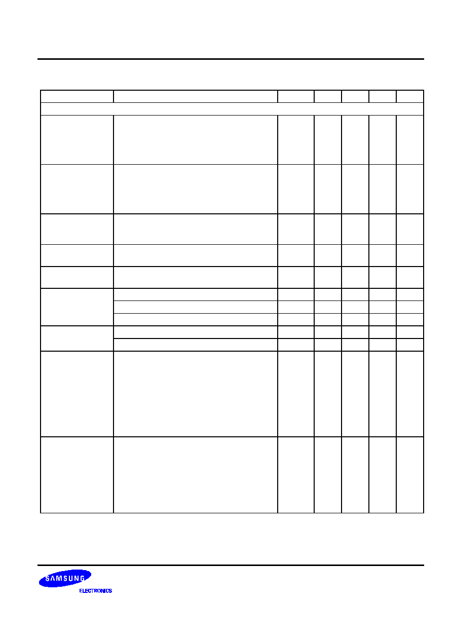
ABSOLUTE MAXIMUM RATINGS
Characteristic
Symbol
Value
Power supply
V
CC
-0.5V to 3.6V
Storage temperature
T
STG
-55
∞
C to +125
∞
C
Operating temperature
T
OPR
-30
∞
C to +85
∞
C
Storage temperature
HBM
±
1500V
Electrostatic discharge rating
MM
±
200V
RECOMMENDED OPERATING CONDITIONS
Characteristic
Symbol
Value
Power supply
Vcc
2.7V to 3.6V
Ambient operating temperature
Ta
-30
∞
C to +85
∞
C
ELECTRICAL CHARACTERISTICS
ELECTRICAL CHARACTERISTICS(V
CC
= 3.3V, Ta = 25
∞
∞
C)
Characteristic
Test Conditions
Symbol
Min
Typ
Max
Units
Current consumption
CDMA idle mode
I
CRX
-
23
33
mA
Current consumption
CDMA sleep mode
I
CSLP
-
300
650
uA
Current consumption
FM idle mode
I
FRX
-
17
26
mA
Current consumption
FM slot mode
I
FSLT
-
4.5
5.5
mA
Current consumption
Power down
I
DWN
-
10
100
uA
Logic high input
V
IH
V
DD
-0.4
-
-
V
Logic low input
V
IL
-
-
0.4
V
Logic high output
V
OH
V
DD
-0.4
-
-
V
Logic low output
V
OL
-
-
0.4
V
Digital input capacitance
C
DI
-
-
5
pF
Digital output load
capacitance
C
DOL
-
-
5
pF
TCXO input impedance
Attach C = 2pF
Z
TCXO
5
-
-
k
CDMA IF input resistance
IF differential
R
IFINC
-
1
-
k
FM IF input resistance
IF single-ended
R
IFINF
-
850
-
IF input capacitance
CDMA, FM IF differential
C
IFIN
-
-
1
pF
VCO input resistance
RX, TX VCO differential
R
VCO
1.8
2
2.2
k
VCO input capacitance
RX, TX VCO differential
C
VCO
-
-
1.5
pF
RX IF/BBA WITH AGC
S1M8656A
7
AC CHARACTERISTICS
Characteristic
Test Conditions
Symbol
Min
Typ
Max
Unit
CDMA Performance
Input sensitivity
Maximum AGC gain. Control input signal so
that output corresponding to 3LSB is output
from ADC. The current source impedance is
500
and matched by connecting a 1k
resistance to the differential input.
VCSEN
-102
-
-
dBm
Maximum input
signal
Minimum AGC gain. Control input signal so
that output corresponding to 3LSB is output
from ADC. The current source impedance is
500
and matched by connecting a 1k
resistance to the differential input.
VCMAX
-
-
-12
dBm
AGC gain slope
PDM is controlled to 3.3V and finds the
differential gain between the control voltage of
1V and 2V.
GSLOPE
33
45
53
dB/V
AGC gain error
over temperature
The difference in gain slope between when the
temperature is -30
∞
C and +85
∞
C.
GVAR
-3
-
3
dB
IF input frequency
range
The IF frequency is increased to find the
frequency where the gain falls below -3dB.
Fin
250
-
-
Mhz
Input power = -102dBm
NFmin
-
7
-
dB
Noise figure
Input power = -75dBm
NFmid
-
20
-
dB
Input power = -25dBm
NFmax
-
70
-
dB
IIP3
AGC gain Max.
IIP3max
-55
-
-
dBm
AGC gain Min.
IIP3min
-10
-
-
dBm
Spurious contents
ADC generated harmonic frequency
component. Two signals in the in-band are
each mixed with signals which will allow ADC
to produce -7dB output signals. The harmonic
and non-harmonic components of the ADC
output signals between 1kHz ≠ 20MHz are
extracted and added. The AGC control
voltage is controlled so that ADC output is full
scale when the input signal is -80dBm.
TSpur
-
-
-25
dBc
Spurious content
related to jammer
In-band spurious peak value produced by IMD
based on 2 jammer signals.
One in-band signal(@50kHz,0.5*F/S)
and two jammers(@900kHz, 22dB*F/S and
@1.7MHz, 21dB*F/S)are simultaneously
input. AGC control voltage is controlled so
that ADC output is F/S when the input signal is
-80dBm.
Jspur
-
-
-18.4
dBc
S1M8656A
RX IF/BBA WITH AGC
8
AC CHARACTERISTICS (Continued)
Characteristic
Test Conditions
Symbol
Min
Typ
Max
Unit
Single-tone
jammer desense
Overall gain reduction due to one jammer.
The in-band signal at -97dBm (control the
AGC control voltage to 0.5*F/S)and the
jammer signal at 900kHz and -57dBm are
simultaneously input. The gain reduces if the
input/output range is small in the BBA.
Jdsen
-
-
1.0
dB
P1dB IF input
level
AGC gain. The input signal level showing 1dB
difference from its idealistic linear line when
the output signal increase, which results from
the input exceeding the output and input
range, starts to saturate.
P1dB
-19
dBm
Crosstalk FM to
CDMA
leakage ratio between CDMA input and FM
input.
CTFC
30
-
-
dB
Offset gain slope
Amount of code change of the voltage ADC
output at the I/Q offset control
GOFS
-
250
-
%FS/V
Offset adjust input
impedance
-
Zoff
100
-
-
k
Out-band
900kHz
ATC9
46
-
-
dB
attenuation
1.2MHz
ATC12
48
-
-
dB
I/Q gain mismatch
Gain mismatch between the I and Q signals
between 1kHz to 615kHz.
Gmis
-1
-
1
dB
I/Q Phase
mismatch
Phase mismatch between the I and Q signals
between 1kHz to 615kHz.
Pmis
-10
10
Deg
Gain flatness
Amount of gain change along I and Q paths
between 1kHz to 615kHz
Gft
-1
1
dB
FM Performance
Input sensitivity
Maximum AGC gain. Control input signal so
that ADC outputs 0.5*F/S. The current source
impedance is 500
and matched by
connecting a 1.2k
resistance to the
differential input.
VSEN
-98.3
-
-
dBm
Maximum input
signal
Minimum AGC gain. Control input signal so
that ADC outputs 0.5*F/S. The current source
impedance is 500
and matched by
connecting a 1.2k
resistance to the
differential input.
VMAX
-
-
-8.3
dBm
AGC gain slope
PDM is controlled to 3.3V and finds the
differential gain between the control voltage of
1V and 2V.
GSLOPE
33
45
53
dB/V
AGC gain error
over temperature
The difference in gain slope between when the
temperature is -30
∞
C and +85
∞
C.
GVAR
-3
-
3
dB

RX IF/BBA WITH AGC
S1M8656A
9
AC CHARACTERISTICS (Continued)
Characteristic
Test Conditions
Symbol
Min
Typ
Max
Unit
IF input frequency
range
The IF frequency is increased to find the
frequency where the gain falls below -3dB.
Fin
85.38
150
MHz
Input power = - 98dBm
NFmin
-
7
-
dB
Noise figure
Input power = - 75dBm
NFmid
-
20
-
dB
Input power = - 25dBm
NFmax
-
70
-
dB
IIP3
AGC gain Max.
IIP3max
-55
-
-
dBm
AGC gain Min.
IIP3min
-25
-
-
dBm
Spurious contents
ADC generated harmonic frequency
component. ADC generated Two signals in the
in-band are each mixed with signals which will
allow ADC to produce -7dB output signals.
The harmonic and non-harmonic components
of the ADC output signals between 1kHz ≠
20MHz are extracted and added. The AGC
control voltage is controlled so that ADC
output is full scale when the input signal is -
80dBm.
TSpur
-
-
-42
dBc
Spurious content
related to jammer
In-band spurious peak value produced by IMD
based on 2 jammer signals.
One in-band signal(@1kHz,0.5*F/S)
and two jammers(@60kHz, 22dB*F/S and
@122kHz, 4dB*F/S)are simultaneously input.
AGC control voltage is controlled so that ADC
output is F/S when the input signal is -80dBm.
Jspur
-
-
-18.4
dBc
Single-tone
jammer desense
Overall gain reduction due to one jammer.
The in-band signal at -93dBm (control the
AGC control voltage to 0.5*F/S)and the
jammer signal at 900kHz and -53dBm are
simultaneously input. The gain reduces if the
input/output range is small in BBA.
Jdsen
-
-
1.0
dB
Crosstalk CDMA
to FM
The leak ratio between the CDMA input and
FM input.
CTCF
30
-
-
dB
Offset gain slope
Amount of code change of the voltage ADC
output at the I/Q offset control
GOFS
250
%FS/V
Offset adjust input
impedance
-
Zoff
100
-
-
k
Out-band
45kHz
ATC9
46
-
-
dB
attenuation
60MHz
ATC12
60
-
-
dB
I/Q gain mismatch
Gain mismatch between the I and Q signals
between 1kHz to 12kHz.
Gmis
-1
1
dB

S1M8656A
RX IF/BBA WITH AGC
10
AC CHARACTERISTICS (Continued)
Characteristic
Test Conditions
Symbol
Min
Typ
Max
Unit
I/Q Phase
mismatch
Phase mismatch between the I and Q signals
between 1kHz to 12kHz.
Pmis
-10
-
10
DegGft
Gain flatness
Amount of gain change along I and Q paths
between 1kHz to 615kHz
Gft
-1
-
1
db
Receive VCO pertormance
VCO and buffered
output Frequency
range
VCO external time constant and PLL value
Fvco
-
170
500
Mhz
VCO phase noise
Tank LC's Q value should be above 20.
Measure @100kHz away from the mid-
frequency.
Pvco
-
-
104
dBc/Hz
RXVCO_OUT
output power
Select a VCO buffer output value reduced by
-2dB. Connect output load to 50
.
Ovco
-15
-
-
dBm
RX IF/BBA WITH AGC
S1M8656A
11
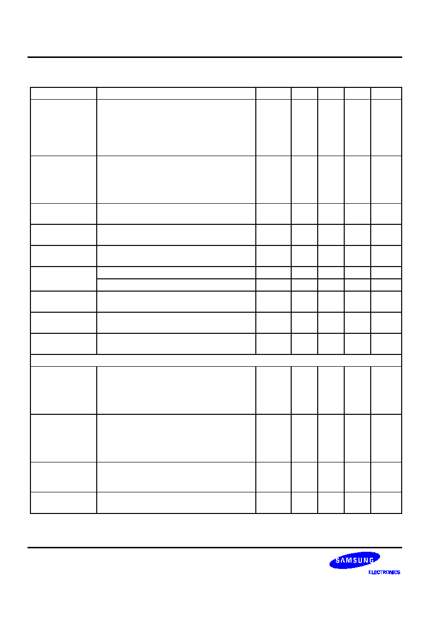
TIMING DIAGRAMS
High time:
50.86 +10ns
CHIPx8 Period: 101.7 ns
High time:
50.86 +10 ns
Falling time:
3 - 12 ns
90%
10%
Rising time:
3 - 12ns
Data hold after CHIPx8
fall > 15ns
CHIPx8
RDO-3
> 20ns
Valid data
Valid data
Valid data
Data output stable prior
to CHIPx8 : > 20ns
Figure1. CDMA Receive ADC Timing
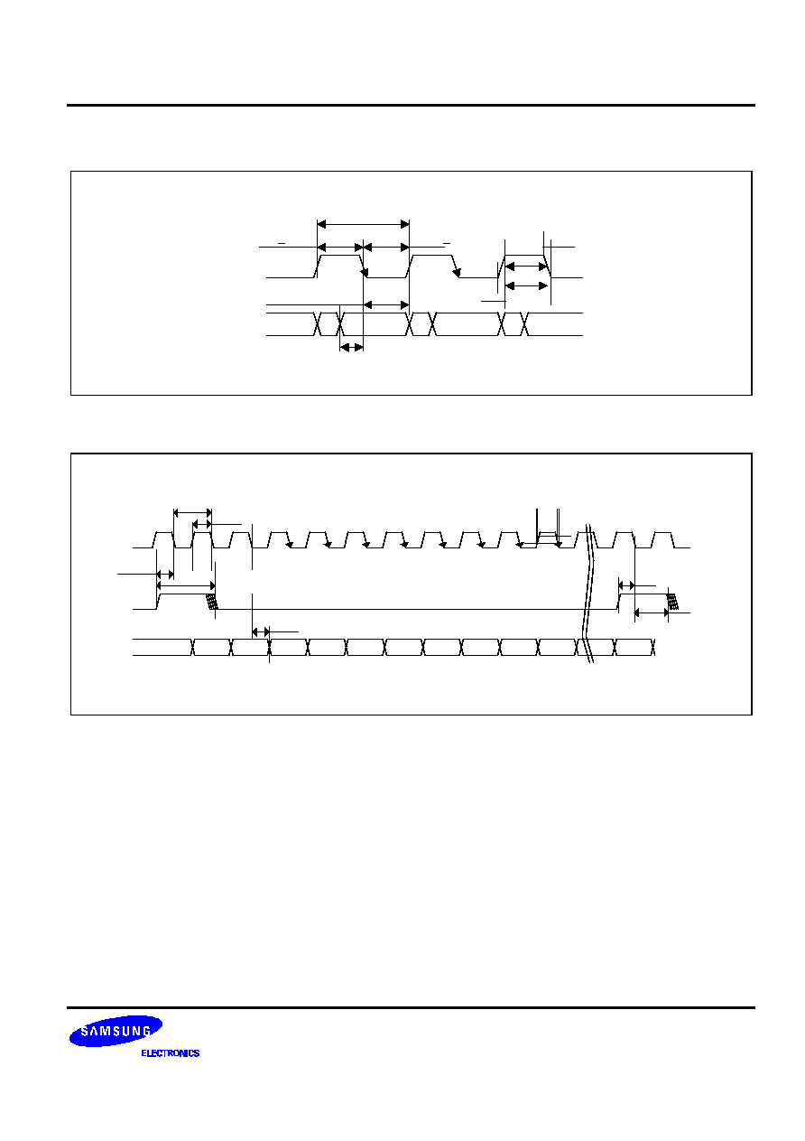
Clock period:
2.78us
Rising time:
3 - 12ns
Falling time:
3 -12ns
High time:
1.39us
Low time:
1.39us
Invalid
FMCLK
FMSTB
FMRXDATA
* All timing specifications is based on C
load
= 12pF, FMCLK=360kHz, FMSTB=40kHz.
D7
D6
D5
D4
D3
D2
D1
D0
90%
10%
Strobe pulse width:
1 - 2.78us
output delay after
clock falling edge: <50ns
Strobe input valid
to clock falling
edge: > 50ns
Strobe input valid
after clock falling
edge: > 50ns
Figure 2. FM Receive ADC Timing

S1M8656A
RX IF/BBA WITH AGC
12
Clock period: 0.6 - 10us
Clock duty cycle: 35 - 65%
CLK
STB
Valid data bit (N)
DATA line hold time:
50 - 200ns
STB line setup time
All data transitions happen while CLK=Low
Clcok N
STB line hold time:
50 - 200ns
DATA
Clcok N+1
Clcok N+2
Valid data bit (N+1)
N+1 Data bit set-up
time : > 50ns
Valid data bit (N+2)
Figure 3. 3-Line Serial Port Interface Timing
Rise time:
3 -12ns
Fall time:
3 -12ns
TCXO/4 period: 101.6ns
TCXO/4 low time:
101.6ns
TCXO/4 high
time: 101.6ns
TCXO
period: 50.8ns
TCXO high time:
25.4ns
TCXO low time:
25.4ns
TCXO input level:
>300mVpp
TCXO/N weak output level:
1.5 - 2.7Vpp
TCXO
TCXO/N
STRONG
OUTPUT
TCXO/N
WEAK
OUTPUT
Figure 4. TCXO and TCXO/N Timing
RX IF/BBA WITH AGC
S1M8656A
13
FUNCTIONAL DESCRIPTION
S1M8656A is a CDMA/AMPS receive-only baseband analog IC, located between the RF mid-frequency
processing terminal and baseband processing terminal. The RF analog mid-frequency signal terminal(IF SAW
filter output), directly connected to the S1M8656A mid-frequency input pin, converts and processes the baseband
signal and sends the corresponding digital signal to the modem IC. Baseband analog processing uses QPSK
modulation, LPF, and A-D converter and the modem IC performs digital CDMA/AMPS baseband modulation on
the digitalized analog baseband signal it receives.
S1M8656A uses a 0.5um BiCMOS, equipped with high-frequency bipolar and low power standardized CMOS
logic, to operate safely in the low power range, consisting of power voltage between 2.7V ≠ 3.6V and operating
temperature between -30
∞
C ≠ +85
∞
C.
CDMA Receive Signal Path
S1M8656A is composed of a receive circuit, installed with TCXO/N, CHIPx8 like clock generator, mode
conversion switch and serial I/F apparatus. The receive circuit has the Rx AGC, an automatic gain controller, and
baseband LPF and output terminal with the A-D converter, and VCO and mixer etc. The input signal is received
as a differential signal, which is modulated to 1.23 MHz spread-spectrum for CDMA. The mid-frequency is
220.38MHz for Korea-PCS, 1.23MHz for US-PCS, and 85.38MHz for cellular; they are set based on the time
constants of the components involved with the external VCO and external Rx PLL. Rx AGC , connected to both
the IF SAW filter and matching component in the RF-IF converter output located in the RF block, amplifies or
reduces according to the signal size. It takes its orders from the modem chip when it sets the appropriate receive
level as required by the CDMA system. Gain is controlled by applying a DC voltage to the RAGC_CONT pin. The
applied DC is produced when the PDM signal, generated as a control signal in the modem, passes through the R-
C filter. The control band of this AGC is approx. 90dB. The QPSK Baseband modulator separates and modulates
the IF signal sent by the AGC using I(In-phase) and Q(Quad-phase) baseband signal. Essentially, two signals, I-
LO and Q-LO (Local oscillator), are mixed with AGC's IF output signals, respectively. The LO(local oscillator)
signal is generated by the internal oscillating components, externally connected tank coil, and Varactor, and the
externally independent PLL device is used to generate its exact oscillation mid-frequency.
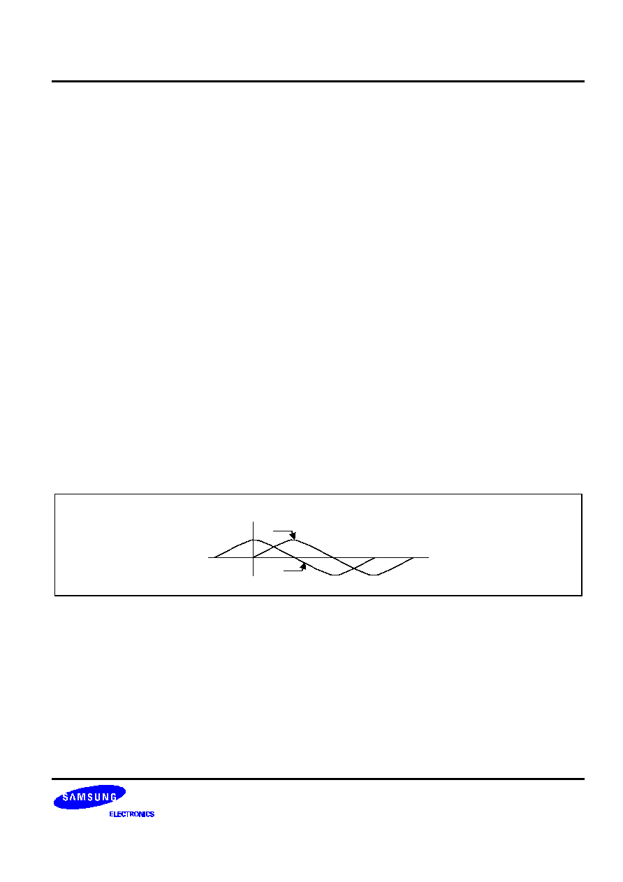
T=0
Q-CH
I-CH
Figure 5. Received I/Q Phase in S1M8656A
Defining of the I-Phase and Q-Phase receive path is very important to its design. The polarities of these paths
are also important to digital baseband modulation. Therefore, the output of the QPSK baseband modulation
determines the I and Q phases; I-phase is defined as the phase leading the Q-phase by exactly 90
∞
, but it simpler
to think of I as Cosin and Q as Sin. The figure related to this is shown in Figure 5. This definition is valid only
when the QPSK IF input signal is higher than the IF mid-frequency. The baseband signal, output by the QPSK
modulator, includes various other unnecessary surrounding band noises, which are removed by the use of the
LPF(Low-Pass-Filter).

S1M8656A
RX IF/BBA WITH AGC
14
Ultimately, I and Q filtered signals are converted to digital signals by the 4-bit A-D converter and sent to the
modem. The A-D converter used is a parallel output type and its outputs are synchronized at the CHIPx8 rising
edge. The modem chip captures the data on the CHIPx8 falling edge. The CHIPx8 clock used in the A-D
converter can change the CHIPx8 output to input so that the clock can be used in systems with different TCXO
reference frequency.
FM Rx Signal Path
S1M8656A FM signal path is the same as that of the CDMA with the exception of a different LPF and A-D
converter, which meet the system specification. Basically a FM modulated signal between IF mid-frequency to
±
15kHz is input so that the baseband LPF, unlike CDMA, has the 12kHz cut-off frequency characteristic. A-D
Converter has 8-bit resolution, characteristic of AMPS, and processing speed of approx. 40kHz. It does not adopt
the power consuming parallel configuration but rather the series configuration to minimize the consumption
power. Regular receive path processing is the same as the BBA except for the separation of the CDMA/AMPS
signal paths. Rx AGC , connected to both the IF SAW filter and matching component in the RF-IF converter
output located in the RF block, amplifies or reduces according to the signal size. It takes its orders from the
modem chip when it sets the appropriate receive level as required by the CDMA system. Gain is controlled by
applying a DC voltage to the RAGC_CONT pin. The applied DC is produced when the PDM signal, generated as
a control signal in the modem, passes through the R-C filter. The control band of this AGC is approx. 90dB. The
QPSK Baseband modulator separates and modulates the IF signal sent by the AGC using I(In-phase) and
Q(Quad-phase) baseband signals. Essentially, two signals, I-LO and Q-LO (Local oscillator), are mixed with
AGC's IF output signals, respectively. The LO(local oscillator) signal is generated by the internal oscillating
component, externally connected tank coil, and Varactor, and the externally independent PLL device is used to
generate its exact oscillation mid-frequency. Defining of the I-Phase and Q-Phase receive path is very important
to its design. The polarities of these paths are also important to digital baseband modulation. Therefore, the
output of the QPSK baseband modulation determines the I and Q phases; I-phase is defined as the phase
leading the Q-phase by exactly 90
∞
, but it simpler to think of I as Cosin and Q as Sin.
T=0
Q-CH
I-CH
Figure 6 Received I/Q Phase in S1M8656A
The figure related to this is shown in Figure 6. This definition is valid only when the QPSK IF input signal is
higher than the IF mid-frequency. The baseband signal, output by the QPSK modulator, includes various other
unnecessary surrounding band noises, which are removed by the use of the LPF(Low-Pass-Filter). The filter pole
is barely 12kHz , merely in the audible range, for AMPS considering that the CDMA is 630kHz. Ultimately, I and
Q filtered signals are converted to digital signals by the 4-bit A-D converter and sent to the modem. The A-D
converter used is a parallel output type ;its outputs are synchronized at the FMCLK and output in the order that it
was synchronized. The modem chip captures the data by matching the FMDATA to the FMCLK clock. The
CHIPx8 clock used in the A-D converter can change the CHIPx8 output to input so that the clock can be used in
systems with different TCXO reference frequency. The clock used by the A-D converter is provided by the
modem chip. It has a 360kHz frequency but can have 40kHz cycle when converting an 8-bit data.

RX IF/BBA WITH AGC
S1M8656A
15
Rx Low-Pass Filters
The CDMA baseband signal frequency can range between 1kHz ≠ 630kHz. Normally, the range between 1kHz ≠
615kHz is called the In-band, between 630kHz ≠ 750kHz Band-edge, and anything outside of these ranges out
band. Very precise characteristics are required in the in-band range. The ripple, I/Q gain-phase error are critical
factors that lead to noise in the in-band. FM Baseband signal ranges between 100Hz ≠ 15kHz. Normally, the
frequency range between 100Hz ≠12kHz is called the in-band, between 12kHz ≠ 18kHz the band-edge, and
anything outside of these ranges the out-band. As for the CDMA, the ripple, I/Q gain-phase error are critical
factors that lead to noise in the in-band.
The LPF characteristic required by these two systems are shown in Figures 7 and 8 below.
Frequency
Frequency
+1.5dB
+0.5dB
0
-1.5dB
-4.0dB
-46.0dB
-48.0dB
1kHz
600kHz
630kHz
750kHz
900kHz
1.2MHz
Relative ammlitued (dB)
Relative ammlitued (dB)
+0.5dB
-0.5dB
-3.0dB
-60.0dB
100hz
12.2khz
18khz
60khz
Figure 7. CDMA Rx Low-Pass Filter Masks
Figure 8. FM Rx Low-Pass Filter Masks
CHIPx8 Clock Generator
CHIPx8 CLOCK is a digital division that divides the 19.68MHz TCXO by 512/1025. It holds the TCXO clock by
half cycle every 512th TCXO cycle and strictly speaking it does not generate 9,8304 MHz precisely. The
9.8304MHz is the mean on the 1025TCXO cycle, where 9.84MHz of 50% duty is obtained from 1 ≠ 512 and 513
≠ 1024. The timing diagram in Figure 9 explains this. The CHIPx8 CLOCK output is held at low when the CDMA
is asleep and FM is idle. Moreover, it can use three division ratios(19.68MHz, 9.84MHz, 9.8304MHz) through the
serial I/F. Various external chip clocks can be used by converting them to inputs.
2/ftcxo
TCXO
CHIPx8
1
2
1023
1024
1025
1026
1027
Figure 9. CHIPx8 Clock form

S1M8656A
RX IF/BBA WITH AGC
16
Rx Voltage Controlled Oscillator(VCO)
S1M8656A includes the Rx LO block having the VCO and quad-phase generator. The quad-phase generator
outputs I-phase and Q-phase clocks with 1/2 the VCO frequency and sends them to the QPSK modulator. The
VCO buffer is used when the VCO output is sent to the external RX PLL. Although the allowable VCO frequency
is determined based on an external time constant, it can only range between approx. 100MHz ≠ 500MHz,
suggesting that the maximum input IF frequency is 250MHz.
Serial Port Interface(SPI)
S1M8656A is equipped with the Serial I/F. All internal functions can be controlled through a common bus using
an external controller. The serial I/F can be used by setting pin 26(SEN) high, the pin which permits/ not permit
the SPI. If the SEN becomes low, the SPI cannot be used and the BBA must be used in the existing BBA 2.0
mode. (All the internal registers are default, which makes the register have the same characteristic as BBA 2.0)
Here, the modem is the master and BBA the slave.
Each pin which uses the SPI bus has the following common functions.
∑
The STB(STROBE) for the serial bus start signal is used to initialize serial data transmission.
This pin is used with the IDLEB function in manual mode and designated the IDLB/STB pin.
∑
Serial BUS DATA is used for the bidirection data input /output at serial data transmission.
This pin is used with the FMB function in parallel mode and designated the FMB/DATA pin.
Because it is an open drain type pin, it requires the pull-up resistance of approx. 8k
.
∑
Serial BUS CLK is used to synchronize the data input/output at serial data transmission.
This pin is used with the SLEEPB function in manual mode and designated the SLEEPB/CLK pin.
S1M8656A can be used to power down the TCXO/N block using the SPI bus when the CDMA is asleep (CDMA
SLEEP). This mode, installed to minimize the product consumption power, is entered by setting a specific bit
(PWRDWN) in the CLK_GEN_MODE register to '1'. The current in the sleep mode reduces from 300uA to
10uA. The SEN(PIN26) pins decide on whether the product will used the SPI bus or parallel control inputs; if it is
in low, then the pins the parallel control input functions, IDLEB, FMB, and SLEEPB, but if in high then these pins
execute the SPI bus functions, STB, DATA, and CLK. This product does not require any external time constants
in initializing the internal register because it can use the internal reset function. Figure. 10 shows the serial bus
connection.
SLOT
STB/IDLEB
CLK/SLEEPB
DATA/FMB
SEN
SEL0/PAON
STB/IDLEB
CLK/SEL1
DATA/FMB
SEN
S1M8656A
S1M8657
SLEEPB
SBST/ADC_ENA
SBCK/ADC_CLK
SBDT/ADC_DATA
PAON
MODEM
V
DD
8k
Figure 10. Serial Bus connection

RX IF/BBA WITH AGC
S1M8656A
17
The advantage of using the SPI bus is the opportunity given to use all the various functions in the product, thus
allowing more flexibility. Moreover, by tieing all the products using a common bus and controlling them together,
the PCB application area and the number of control pins for the master can be simultaneously reduced, as
compared to controlling the products independently.
Serial Port Interface Operation
The modem, the master, controls slaves such as S1M8656A using the SPI bus.
The STB falling edge indicates the start of the serial I/F data transmission. The STB becomes high to mark the
end of the data transmission.
(Data sent after the STB turns high are not valid.)
Serial line data is captured and stored as soon as the BBA or the MODEM places the clock on the falling edge.
The SPI 3-line must remain high for at least 1-clock cycle in order to sent new data.
The MSB always outputs the data line data.
After 9-clocks, which is required to send data, the data line driver opens the data line, at which time the data line
becomes high because of the external pull-up resistance.
Serial Data Transfer format
S1M8656A and S1M8657 are all slave devices with the SPI bus. What differentiate them from one another is
their different device IDs. Each company has its own characteristic SPI bus configuration , but normally the 3-line
bus is most often used and sometimes the 2-line bus such as the IIC bus.
Figure 11. shows the serial data transfer format.
mode=01
Dummy
1=Master read
Master drive
Slave Address
Start bit
STB
CLK
DATA
D5 D4 D3 D2 D1 D0
D6 D5 D4 D3 D2 D1 D0
D7 D6 D5 D4 D3 D2 D1 D0
D6 D5 D4 D3 D2 D1 D0
D7 D6 D5 D4 D3 D2 D1 D0
Master drive
Register
Address
Slave drive
data
Master drive
Register
Address
Master drive
data
End bit
Dummy
Dummy
0=Master read
Dummy
Dummy
Figure 11. Serial Data Transfer Format
(1) The first 2-BITs are for transmission only and this product must send '01'.(Others are not permitted.)
(2) The following 6-bit data specifies the slave device, which is connected to the SPI bus and has its own ID.
(3) The following 1-bit is a dummy bit, which marks the end of the 8-bit data transmission and the beginning of
the next data to be sent.
(4) The following 1-bit decides on whether the master will drive the data line or the slave will. If this bit is '1', the
master will drive , but if '0' the slave will drive the data line.
(5) The following 7-bit data is the register address of the specified slave device; the 7-bits for an address allows
128 register addresses for slaves.
(6) The following high 1-BIT data is a dummy data.
(7) The following 8-BIT data is the data in the device to be driven.

S1M8656A
RX IF/BBA WITH AGC
18
(8) The following 1-BIT data is a dummy data, which marks the end of the 8-bit data transmission and beginning
of the next data to be sent.
(9) The following 1-bit decides on whether the master will drive the data line or the slave will. If this bit is '1', the
master will drive , but if '0' the slave will drive the data line.
(10) The following 7-bit data is the register address of the specified slave device.
(11) The following high 1-BIT data is a dummy data.
(12) The following 8-BIT data is the data in the device to be driven.
(Continous data transmission such as this can be ended with a 1-byte transmission or can be read/written
repeatedly.)
(13) After the last data is sent, the data line opens and becomes high;
(14) the CLK continues for half the 1-clock cycle and then becomes high;
(15) and the STB becomes high as soon as the clock becomes high and this marks the end of data transmission.
Modes of Operation
S1M8656A can be controlled by existing parallel control inputs such as BBA 2.0 or by the SPI bus.
The modes of operation consists of digital state FMB, IDLEB, and SLEEPB modes; Table 2 shows the various
modes.
Table 2. Mode control in the Parallel mode control
Mode
FMB
IDLEB
SLEEPB
CHIPx8
TCXO/N
CDMA talk
H
H
H
On
On
CDMA idle
H
L
H
On
On
CDMA sleep
H
L
L
Off
On
FM talk
L
H
X
On
On
FM idle
L
L
H
Off
On
Rx slot
L
L
L
Off
On
A Rx slot which is not in the existing BBA is shown in the table above. This function was installed for the new FM
Slotted mode. The reason for this new slot is simple. All users are aware of the need to quickly convert from the
sleep mode to the idle mode and that PLL related functions are the slowest to set-up. This is because the PLL
incorporates many external time constants and the large capacitor that is includes takes a long time to charge
and discharge. As one measure, the external time constant could be changed or PLL related blocks could be left
on completely. Here, the Rx slot function in the BBA leaves the VCO completely on. The Rx slot function leaves
the Rx VCO on only when IDLEB is low, SLEEP is low and FMB is low, but an additional 4.5mA of current is
consumed. Even if the RXSLOTB is low in the FM idle mode, remains in the FMSLOT mode.
RX IF/BBA WITH AGC
S1M8656A
19
CONTROL REGISTERS
S1M8656A has various registers which can be programmed by the SPI bus. These registers have their own
function which are described below.
Table 3. S1M8656A Control Registers
Register name
Address
R/W
Default vale
Description
RESET
0x00
W
-
Reset.
Reset S1M8656A and all the register values are returned
to their default value.
SPI_ID
0x01
R
0x1F
SPI_ID.
Each slave device has its own, independent code;
S1M8656A code is 1Fh.
Not applied
0x02
Not used.
BLOCK_CTL
0x04
R/W
0x3C
BLOCK_CTL
Decides on the S1M8656A operation and performs the
same functions as IDLEB, FMB and SLEEPB in the
parallel control mode.
Not applied.
0x06
Not used.
CLK_GEN_MODE
0x09
R/W
0x0C
CLK_GEN_MODE
Changes the internal divider(TCXO,CHIPx8) conditions;
controls the output drive.
Not applied.
0x0A
Not used.
AGC_DCONV
0x0C
R/W
0x0B
AGC_DCONV
Controls the AGC gain control range and VCO output.
Not applied.
0x0E
Not used
Reserved
0x10
Absolutely not permitted.
Reserved
0x11
W : MODEM is recorded in the S1M8656A register R : When S1M8656A sends data to the modem
Table 4. Description Of Control Registers
ADDRESS
NAME
TYPE
BITS
Description
00
RESET
W
-
When the master uses this register, the S1M8656A returns
all the programmed register values to their initial value.
01
SPI_ID
R
[5:0]
This read-only register is used to confirm the type of slave
connected to the master. It is set to 1Fh and all
S1M8656A has the same value. This is the ID absolutely
required to differentiate the controller from the data, when
there are many slaves connected to the SPI bus.
S1M8656A
RX IF/BBA WITH AGC
20
Table 4. Description Of Control Registers(Continued)
ADDRESS
NAME
TYPE
BITS
Description
[7:5]
Reserved. Default = 001
[4]
Reserved. Default = 1
[3]
Reserved. Default = 1
04
Block_CTL [4:0]
R/W
[2]
FMB. Default = 1
1: CDMA Mode, 0: FM Mode
CDMA Mode or FM Mode select bit.
[1]
IDLEB. Default = 0
1: RxTx Mode, 0: Idle Mode
Talk Mode or idle Mode select bit.
[0]
SLEEPB. Default = 0
1: follows the IDLEB state. 0: SLEEP Mode
SLEEP or None-SLEEP select bit.
When [2:0] = 001 and RXSLOTB=0, FMSLOT Mode; if RXSLOTB = 1,FM Rx
Mode.
If [2:0]=000, becomes FMSLOT Mode, regardless of RXSLOTB. Operates in the
CDMA Mode, regardless of the RXSLOTB state.
[7:5]
Reserved. Default = 000
[4]
TCXO_PWR. Default = 0
1: TCXO/N output not allowed
0: TCXO/N output allowed
TCXO/N division and output permit/not permit select bit.
09
CLK_GEN_
MODE [4:0]
R/W
[3]
TCXO_DRV. Default = 1
1: TCXO/N Weak CMOS output
0: TCXO/N is STRONG CMOS output
TCXO/N DRIVE select bit according to conditions of use.
[2]
TCXO_N. Default = 1
1: TXCO/N ; N = 4
0: TCXO/N ; N = 1
TCXO/N output division ratio selection parameter.
[1:0]
CHIPx8. Default = 00
00: In the Normal Mode, it has the TCXO*512/1025 ratio.
01: CHIPx8 output is converted to external clock input.
10: Half the TCXO is output.
11: CHIPx8 division and output are not allowed.
Select bit on whether to use the CHIPx8 division ratio with the
input mode or output mode.

RX IF/BBA WITH AGC
S1M8656A
21
Table 4. Description Of Control Registers (Continued)
ADDRESS
NAME
TYPE
BITS
Description
[7]
Reserved. Default = 0
[6:5]
AGCPDM. Default=00. AGC PDM control range
00: PDM 3.3V : Use when VDDM = 3.3V
01: PDM 2.4V : Use when VDDM = 2.4V
10: PDM 2.7V : Use when VDDM = 2.7V
11: Reserved : not allowed.
Reserved bit for changes to PDM voltage according to the
MODEM power voltage BIT.
[4]
Reserved. Default = 0
0Ch
AGC_RVCO
[5:0]
R/W
[3]
AGCPON. Default=1. RX AGC power control
1: Power on : allows AGC
0: Power down mode : not allow AGC .
[2]
RVCOLVL. Default=0. RXVCO output level control
1: Outputs RXVCO_OUT normally.
0: Reduces RXVCO_OUT by -2dB.
Bit to eliminate the harmonic component that can be caused by
RX VCO.
[1:0]
RVCO. Default = 11.
00: All block Power down, excluding TCXO/N.
01: Mode that forces external VCO in the VCO Tank.
10: Mode that forces external VCO in the VCO Tank.
11: Normal VCO Mode.
VCO operating mode defining bit.
S1M8656A
RX IF/BBA WITH AGC
22
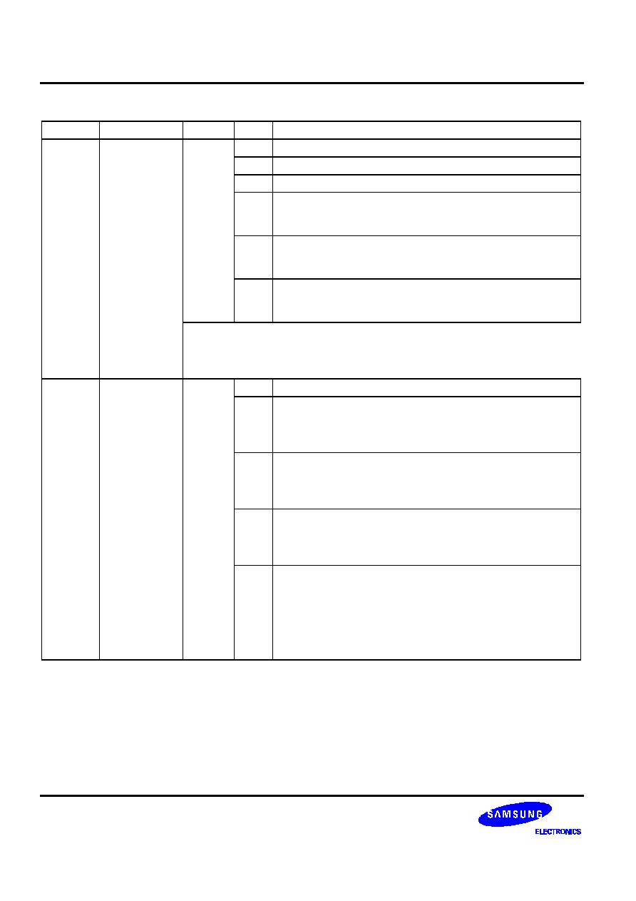
CHARACTERISTIC GRAPH
10
100
1K
10K
100K
1M
-120
Phase noise(dBc/Hz)
-110
-100
-90
-80
-70
-60
-50
-40
-30
Frequency offset(Hz)
GRPH 2-1 S1M8656A01 VCO Open Loop Phase Noise at RXVCO_OUT
Input Power(dBm)
Vcntl(V)
0
-20
-60
-80
-100
-40
0.0
0.5
1.0
1.5
2.0
2.5
3.0
Rs=3.3K/PDM=3.3V
for CDMA full-scale output.
GRPH 2-2 S1M8656A01 Input Power vs. Vcntl Performance
GRPH 2-2 S1M8656A Input Power vs. Vcntl Performance
for CDMA full-scale output.
GRPH 2- 1 S1M8656A VCO Open Loop Phase Noise at
RXVCO_OUT
0
-100
-80
-60
-40
-20
0
-10
-20
-30
-40
-50
Pin(dBm)
IIP3(dBm)
Rs=3.3K/PDM=3.3V
GRPH 2-4 S1M8656A01 IIP3 for CDMA half-scale output
Rs=3.3K/PDM=3.3V
Noise Figure(dB)
Input Power(dBm)
-105 -100 -95
-90
-85
-80
-75
-70 -65
4
6
8
10
12
14
16
18
GRPH 2-3 S1M8656A01 CDMA Noise Figure
GRPH 2- 4 S1M8656A IIP3 for CDMA half-scale output
GRPH 2- 3 S1M8656A CDMA
Noise Figure
RX IF/BBA WITH AGC
S1M8656A
23
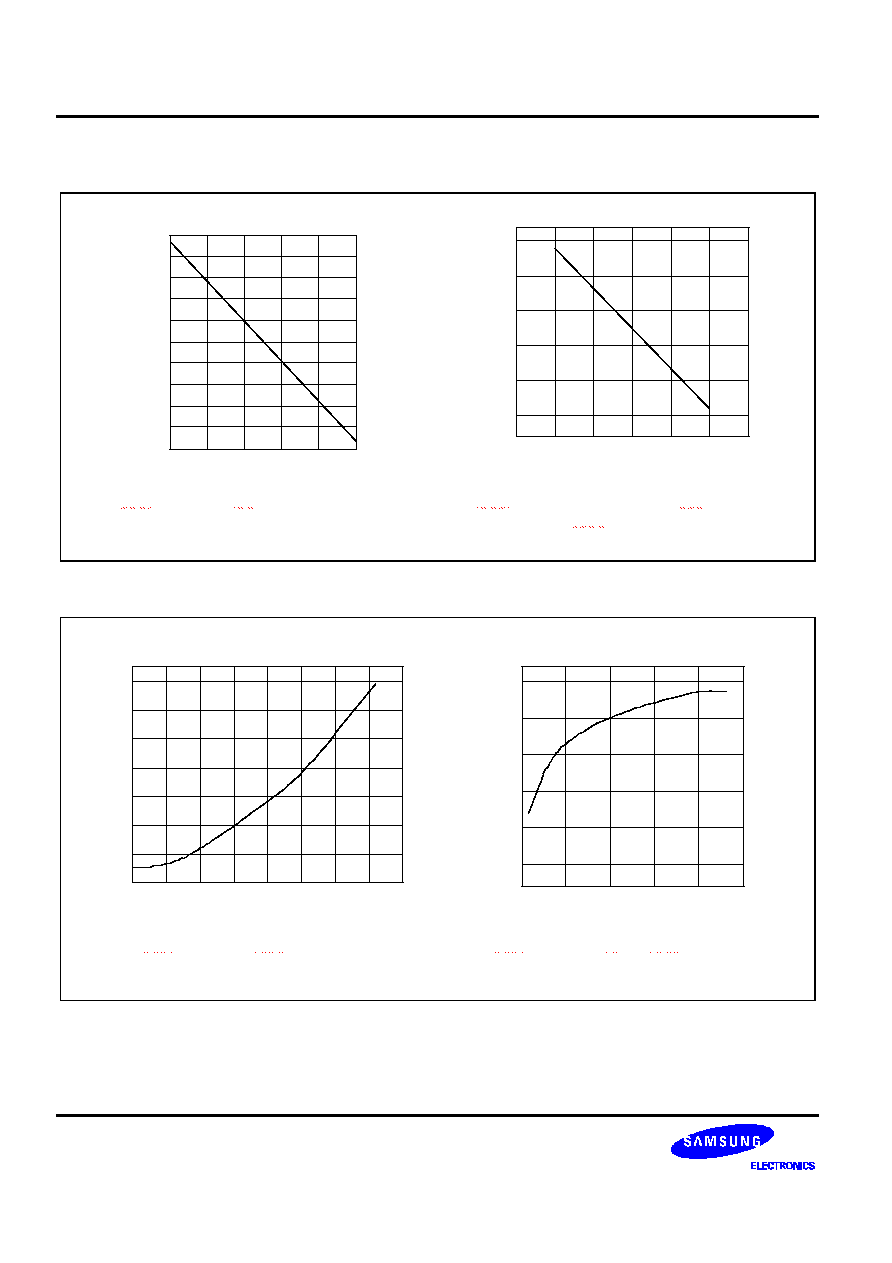
CHARACTERISTIC GRAPH (Continued)
Input Power(dBm)
Vcntl(V)
0
-20
-60
-80
-100
-40
0.0
0.5
1.0
1.5
2.0
2.5
3.0
Rs=3.3K/PDM=3.3V
for FM full-scale output.
GRPH 2-5 S1M8656A01 Input Power vs. Vcntl Performance
Rs=3.3K/PDM=3.3V
Noise Figure(dB)
Input Power(dBm)
-105 -100 -95
-90
-85
-80
-75
-70 -65
4
6
8
10
12
14
16
18
GRPH 2-6 S1M8656A01 FM Noise Figure
GRPH 2- 5 Input Power vs. Vcntl Performance
for FM full-scale output.
GRPH 2-6 S1M8656A FM Noise Figure
0
-100
-80
-60
-40
-20
0
-10
-20
-30
-40
-50
Pin(dBm)
IIP3(dBm)
Rs=3.3K/PDM=3.3V
GRPH 2-7 S1M8656A01 IIP3 for FM half-scale output
GRPH 2-7 S1M8656A IIP3 for FM half-scale output
S1M8656A
RX IF/BBA WITH AGC
24
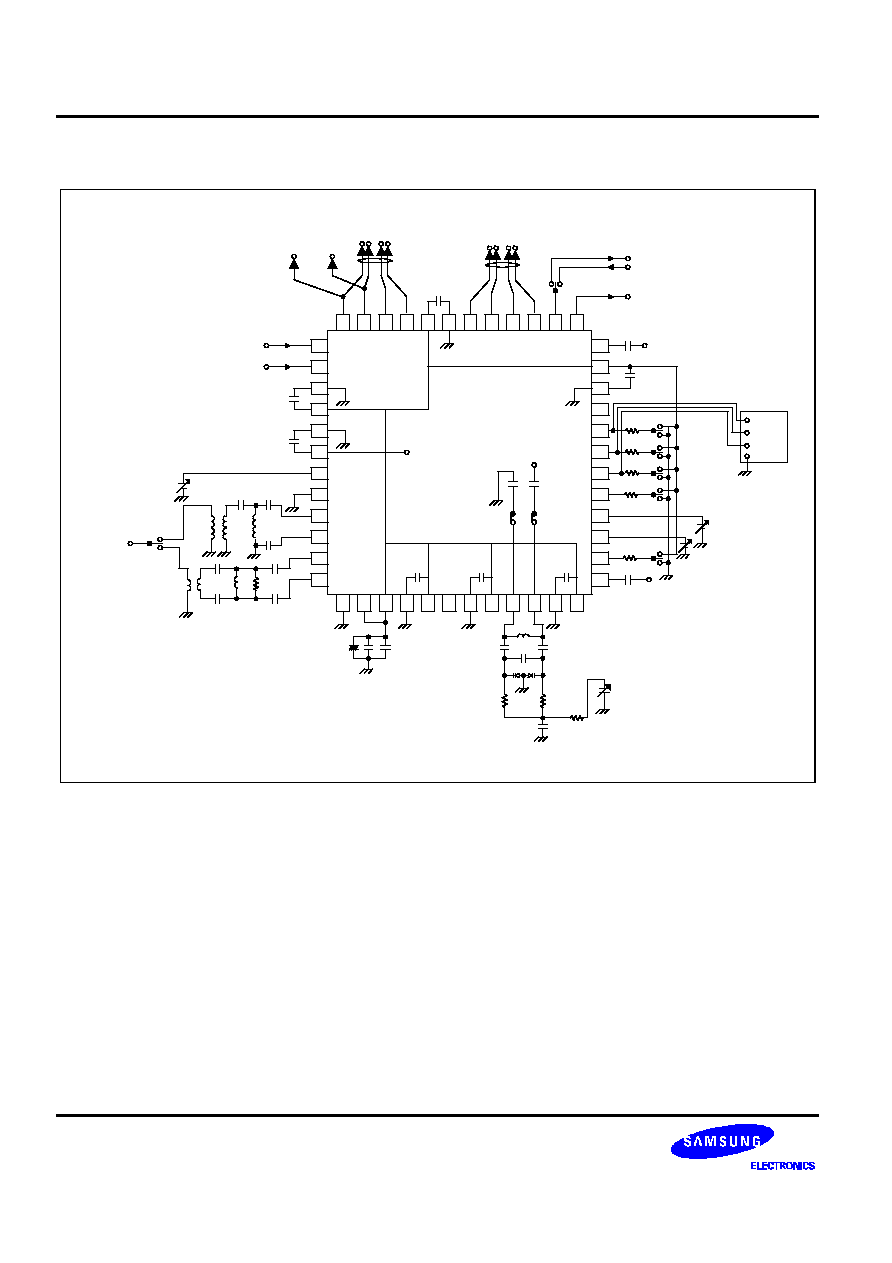
TEST CIRCUIT
VCON
VIF
FM
SW_MODE
10nF
10nF
VCC
VCOIN
S1M8656A
FMCLK
FMSTB
1
2
3
4
5
6
7
8
9
10
11
12
13
14
15
16
17
18
19
20
21
22
23
24
36
35
34
33
32
31
30
29
28
27
26
25
48
47
46
45
44
43
42
41
40
39
38
37
CD
SW_SLP
SW_FM
SW_IDL
SW_ST
CLK
DATA
STB
10nF
10nF
10nF
1nF
1nF
SW_VCO
10nF
2pF
2.3nH
10nF
10nF
10nF
2.3nH
2pF
2pF
1:8
1:8
1uF
1nF
10nF
100nH
47pF
47pF
1SV229
10K
10K
1nF
10K
VTUN
1nF
SW_SEN
VQOFS
22K
SEN
VIOFS
R=22K
SLOTB
IDLEB
FMB
SLEEPB
10nF
TCXOIN
1nF
TCXOIN
E_CHIPX8
CHIPX8
SW_CHIP
CDMA_QD
10nF
QD3
QD2
QD1
QD0
ID3
ID2
ID1
ID0
CDMA_ID
FM_ID
FM_QD
RX IF/BBA WITH AGC
S1M8656A
25
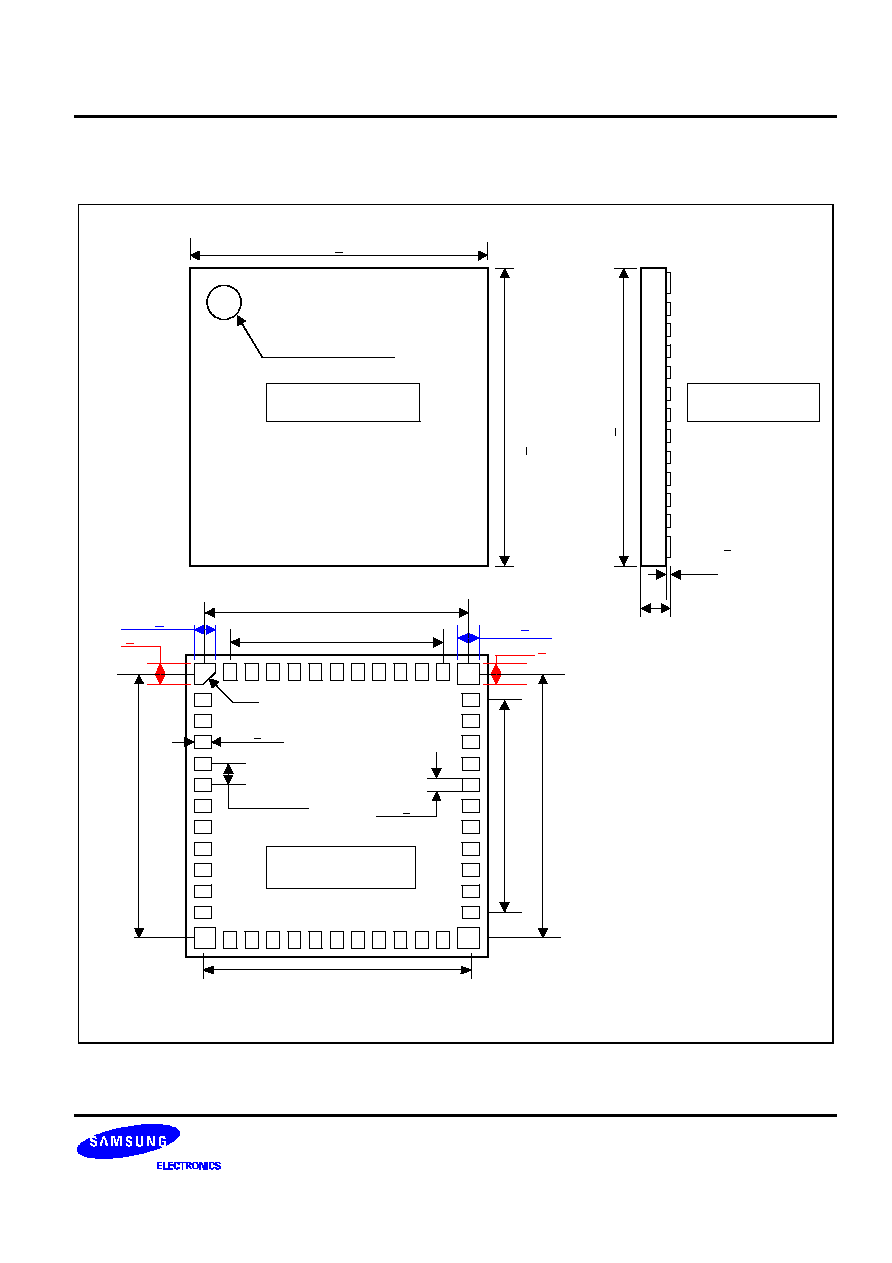
48BCC PACKAGE OUTLINE
#1 INDEX LASER MARK
UNIT:mm
C0.2
6.15
TYP
6.15 TYP
5.0 TYP
0.50 TYP
7.00 + 0.10
#37
#25
7.00
+
0.10
#13
#1
TOP VIEW
#1
#13
#25
#37
0.40
+ 0.10
0.30
+ 0.10
BOTTOM VIEW
0.045 + 0.10
0.045 + 0.10
0.045 + 0.10
0.045 + 0.10
6.15 TYP
6.15 TYP
5.0 TYP
7.00
+
0.10
SIDE VIEW
0.085
+ 0.040
Stan off
0.80 MAX
Total height

S1M8656A
RX IF/BBA WITH AGC
26
PACKAGE DIMENSION
48LQFP PACKAGE OUTLINE
#48
7.00
+ 0.20
9.00
+ 0.30
7.00
+
0.20
9.00
+
0.30
0.10 MAX
0.127
+ 0.010
- 0.005
0-8
NOTE: Dimensions are in millimeters.
#1
0.18
+ 0.10
- 0.05
0.50
(0.75)
0.50 - 0.20
0.05 MIN
1.40
+ 0.10
1.60 MAX