TX IF/BBA WITH AGC
S1M8657
1
INTRODUCTION
S1M8656A/8657 are CDMA/AMPS Dual Mode IF/ baseband IC which is
divided into three main parts - IF frequency processing, baseband
processing , and digital interface. The receiver IC (S1M8656A) and
transmitter IC (S1M8657) are provided as a KIT.
S1M8656A is a receiver IC, installed with a Rx AGC, Baseband
Converter, Baseband analog filter, and A-D Converter. It can send a
digital baseband signal to the digital baseband IC. The S1M8657 is a
transmission-only IC, installed with a Tx AGC, IF frequency converter,
analog filter, D-A Converter, PLL, 8-bit A-D Converter for the system
monitor, and 3-input analog switch. It connects the digital baseband IC to
the RF processing. Designed to operate in direction connection with the
MSM, S1M8656A and S1M8657 are fabricated on the Samsung's 0.5um
high-speed, high-frequency BICMOS processing and can achieve
superior high frequency and low power digital operations.
Its operating voltage is 2.7V ≠ 3.6V, and operating temperature
-30
∞
C ≠ +85
∞
C.
FEATURES
∑
CDMA/AMPS Dual Mode
∑
AGC output signal range : 90dB
∑
Built-in QPSK baseband to IF converter
∑
Built-in Tx I and Q LPF
∑
Built in I,Q 8-BIT DAC
∑
Built-in programmable Tx IF PLL
∑
Built-in VCO for QPSK converter and IF conversion
∑
Built-in 8-BIT GP ADC with 3-input analog switching
∑
Built-in 3-line Serial Port Interface (SPI)
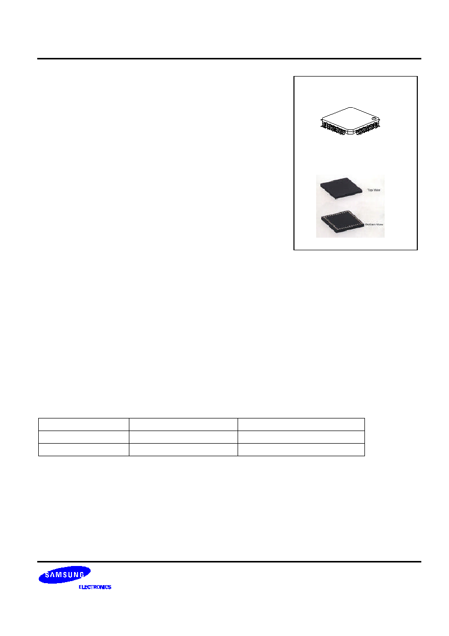
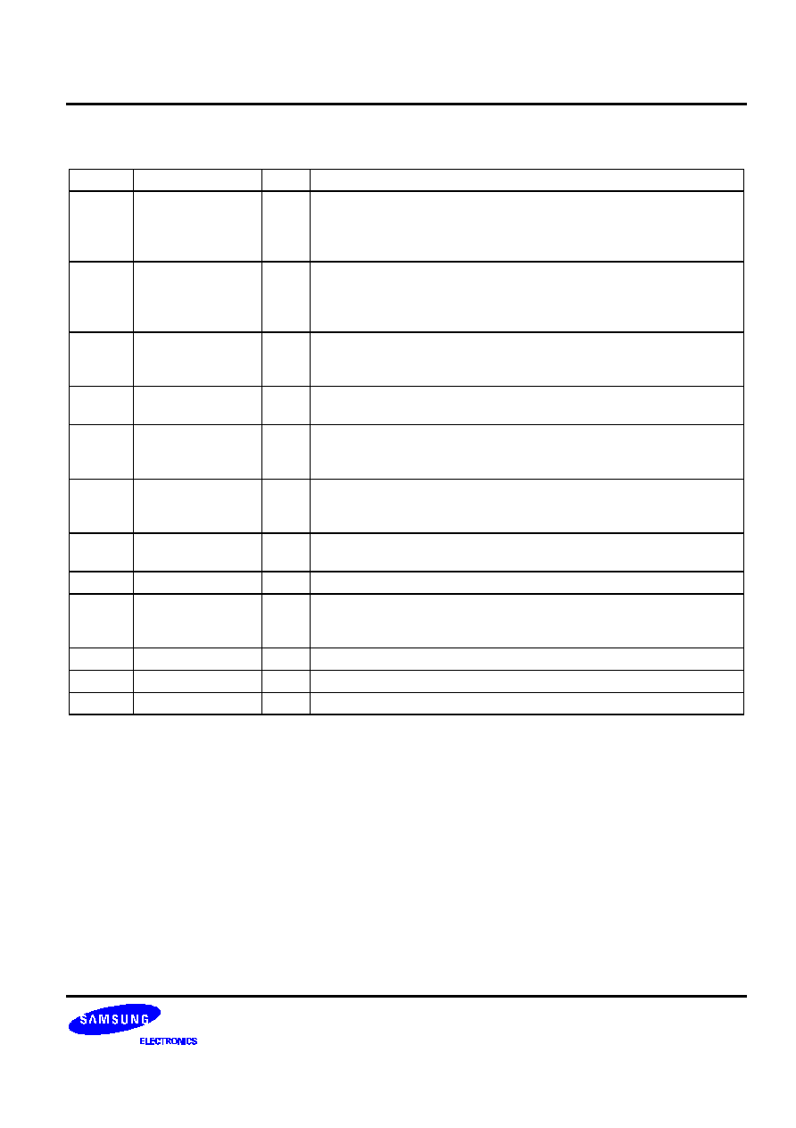
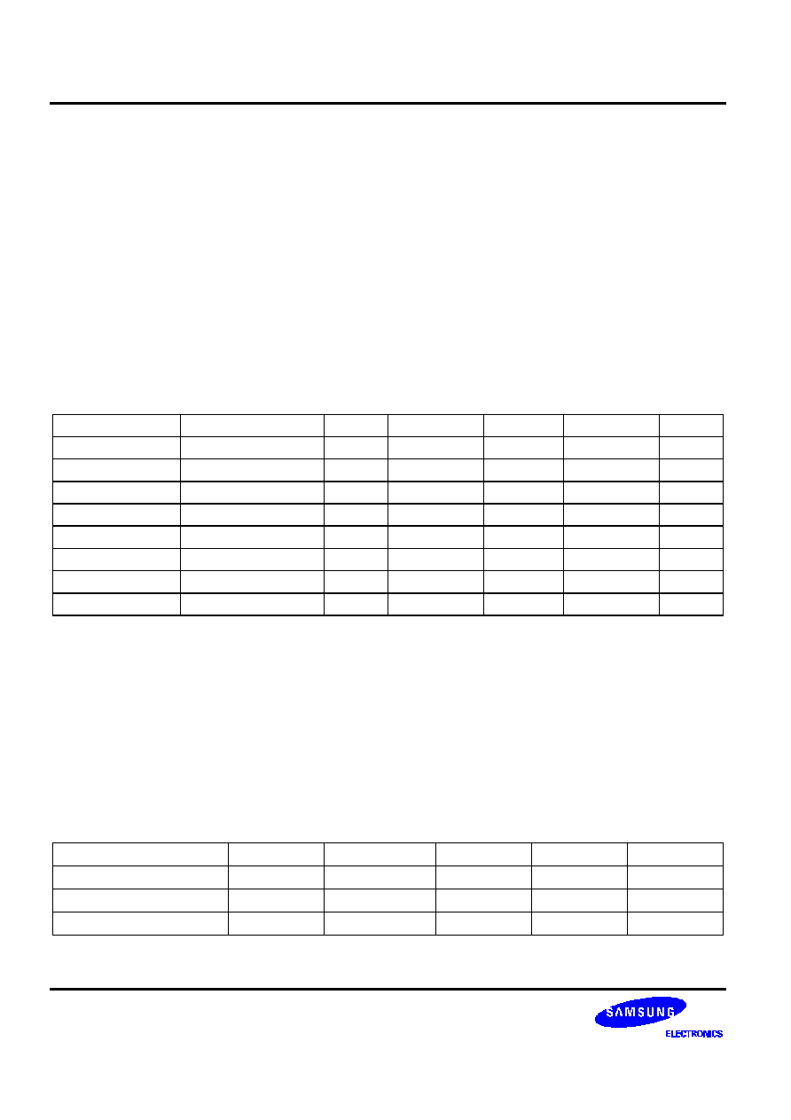
ORDERING INFORMATION
Device
Package
Operating Temperature
+ S1M8657X01-E0T0
48-LQFP-0707
-30 to +85
∞
C
+ S1M8657X01-F0T0
48-BCC-7.0
◊
7.0
-30 to +85
∞
C
+: New product
48-BCC-7.0
◊
7.0
48-LQFP-0707
S1M8657
TX IF/BBA WITH AGC
2
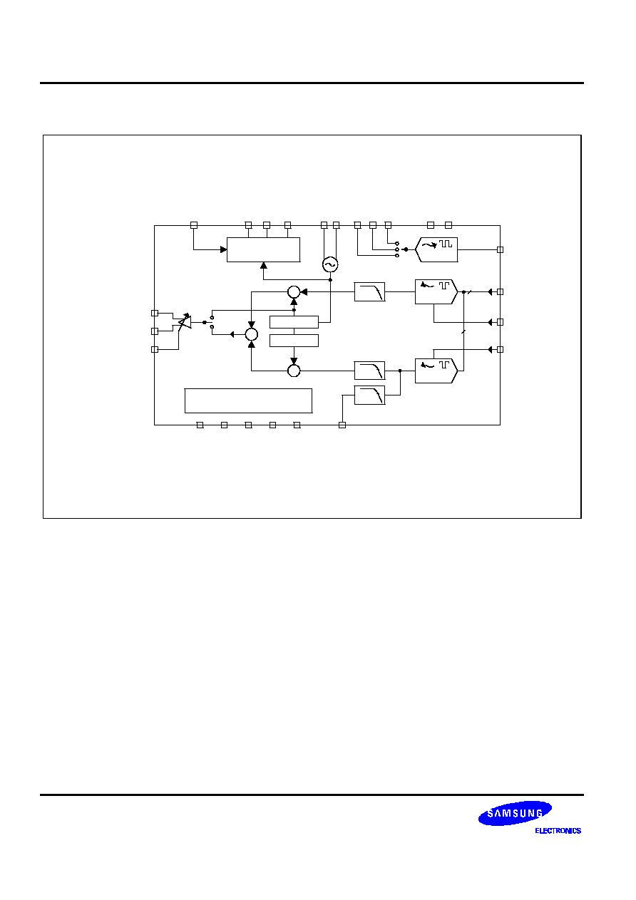
BLOCK DIAGRAM
ADC
8
IDLEB/STB
SMSB/CLK
SLSB/PAON
SEN
FM_MOD
GPDATA
TXD0-7
TCLK
TCLKB
TX_IF1
TX_IF2
TAGC_CONT
TCXO
TX_VCO_T1
TX_VCO_T2
GPIN1
GPIN2
GPIN3
GPENA
GPCLK
FMB/DATA
PDISET
PDOUT
LOCK
+
x
1/2 DIV.
90D-PSN
x
TX-PLL
Synthesizer
8
LPF
LPF
LPF
DAC
DAC
3-line Serial Port Interface
Mode control
TX IF/BBA WITH AGC
S1M8657
3
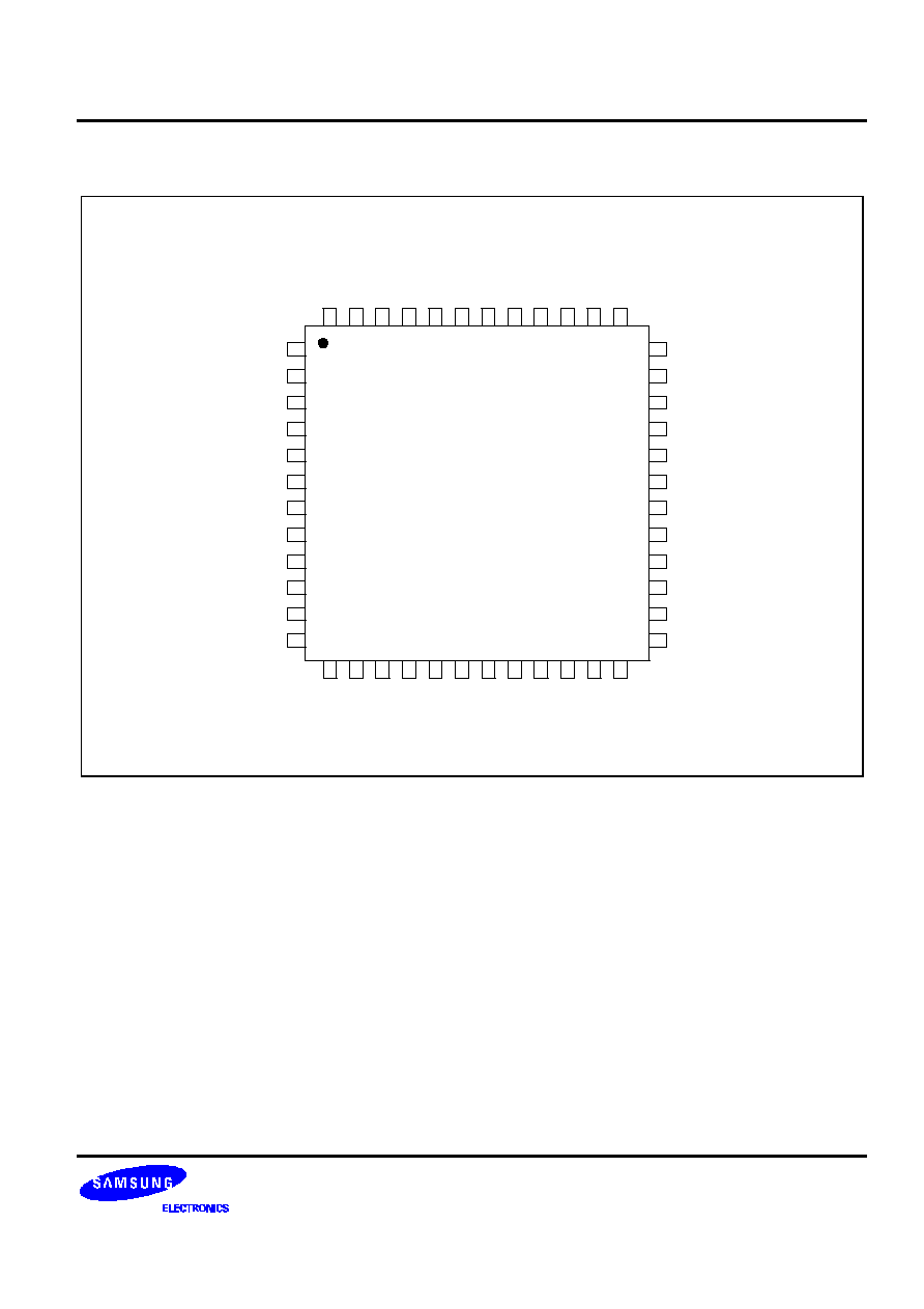
PIN CONFIGURATION
GND
GND
VCC
TX_IF1
TX_IF2
TAGC_CONT
GND
N.C
VCC
GND
TXD0
TXD1
TXD2
TXD3
TXD4
TXD5
TXD6
TXD7
TCLK
TCLKB
VDDM
GND
VCC
GPENA
GPDATA
GPCLK
GPIN1
GPIN2
GPIN3
SMSB/PAON
SEN
FMB/DATA
IDLEB/STB
SLSB/CLK
TCXO
LOCK
PDISET
PDOUT
GND
VCC
FM_MOD
TXVCO_T1
TXVCO_T2
GND
VCC
N.C
VCC
GND
1
2
3
4
5
6
7
8
9
10
11
12
13
14
15
16
17
18
19
20
21
22
23
24
36
35
34
33
32
31
30
29
28
27
26
25
48
47
46
45
44
43
42
41
40
39
38
37
S1M8657
S1M8657
TX IF/BBA WITH AGC
4
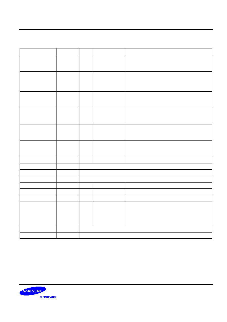
PIN DESCRIPTION
PIN
NAME
I/O
Description
1
2
TX_IF1
TX_IF2
AO
Outputs differential signal to the IF output signal pin. Output format is
an open-collector. Only operates in the CDMA/FM talk mode. An
external components pull it up using VDD when operation is not
allowed.
4
TAGC_CONT
AI
DC input for AGC gain control. This input is the PDM control signal
from the modem, which was converted to a digital signal in the R-C
filter. This pin has high impedance when not in operation.
8
N.C
-
Not used in this product.
11
12
13
14
15
16
17
18
TXD0
TXD1
TXD2
TXD3
TXD4
TXD5
TXD6
TXD7
DI
Transmit data input pins for transmit 8-bit D/A converter TXD7 is the
MSB.
19
20
TCLK
TCLKB
DI
Complementary inputs to transmit D/A converter.
24
GPENA
DI
This pin is always on stand-by and is not affected by the SEN's pin
conditions. If this pin changes from low to high when the TCXO is
allowed, GP-ADC starts to operate as well as GPDATA and GPCLK.
25
GPDATA
DO
GP-ADC conversion data output pin. This pin cannot be operated by
the SPI but must be operated by the GPENA pin. On stand-by, the pin
is at low.
26
GPCLK
DO
GP-ADC conversion data synchronization pulse output pin. This pin
cannot be operated by the SPI but must be operated by the GPENA
pin. On stand-by, the pin is at low.
27
28
29
GPIN1
GPIN2
GPIN3
AI
3-analog input terminals. Only the input from one of these is input to
the GP-ADC. The input is selected based on the conditions of the
SMSB/PAON and SLSB/CLK terminals in the SPI restrict mode and
on the register value in the SPI operating mode. On stand-by, it has
high impedance.
30
SMSB/PAON
DI
SEN is the pin for the former bit of the two bits used to select the GP
input in low state. This pin executes the PAON function when SEN=1
and TXMODE_CONT[3] =1 and executes the Tx Puncture mode when
this pin is at low.
31
SEN
DI
Select pin for the use of the SPI BUS. If this pin is at high, the SPI bus
can be used; if low, the SPI bus cannot be used but an external
control pin can be used.
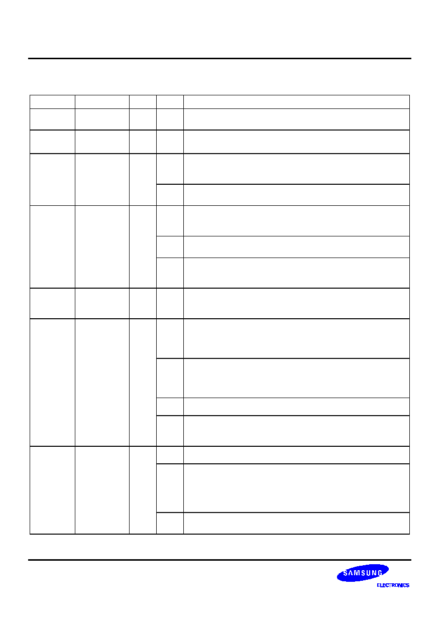
TX IF/BBA WITH AGC
S1M8657
5
PIN DESCRIPTION (Continued)
PIN
NAME
I/O
Description
32
FMB/DATA
BI
When SEN = high, this pin is used as the SPI data input pin; when
low, it converts to the FMB, the parallel control input. In the parallel
control mode, if this pin becomes low, the IC enters FM Mode and, if
high, CDMA Mode.
33
IDLEB/STB
DI
When SEN = high, this pin is used as the SPI STB(Strobe) pin; when
low, it converts to IDLEB, the parallel control input. In the parallel
control mode, if this pin becomes low, the IC enters the IDLE mode,
and if high, TALK mode.
34
SLSB/CLK
DI
When SEN = high, this pin is used as the SPI CLK input pin; when
low, it converts to the SLSB, the parallel control input and becomes
the input pin for the latter bit of the two GP input select bit.
35
TCXO
AI
External TCXO signal input pin, whose input DC potential is 1.5V from
only the input bias when not operating.
37
PDISET
AO
Pin determining the charge pump current in the PLL, whose operating
voltage is 0.64V. The resistance between this pin and GND
determines the charge-pump current, which is R/0.64.
38
PDOUT
AO
Charge pump current output pin, whose peak current is R/0.64 and
11R/0.64 in the Lock mode and Acquisition mode, respectively. When
not operating, it is at high impedance.
41
FM_MOD
AO
FM modulation FM Baseband output signal, which is sent only in the
FM Talk mode but has high impedance at any other time.
6, 45, 47
VDD
Power pin for the analog circuit.
3, 5, 7,
22, 39,
44, 48
GND
Ground pin for the analog circuit.
21
VDDM
Pin for the digital input/output circuit connected to the modem.
9, 23, 40
VDD_DIG
Digital logic power pin.
10
GND_DIG
Digital circuit ground pin.
S1M8657
TX IF/BBA WITH AGC
6
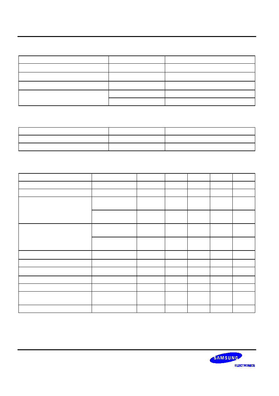
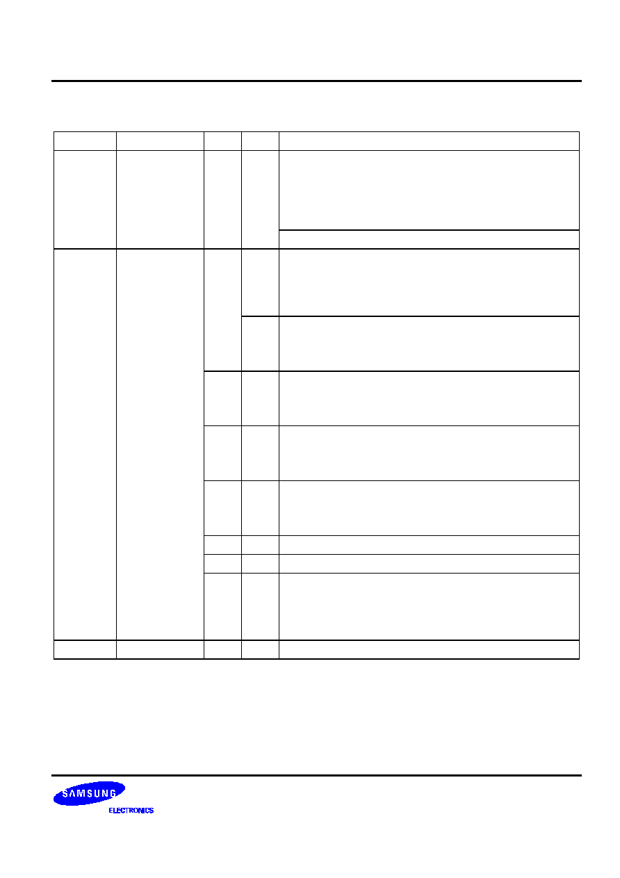
ABSOLUTE MAXIMUM RATINGS
Characteristic
Symbol
Value
Power supply
V
CC
-0.5V to 3.6V
Storage temperature
T
STG
-55
∞
C to +125
∞
C
Operating temperature
T
OPR
-30
∞
C to +85
∞
C
Electrostatic discharge rating
HBM
±
1500V
MM
±
200V
RECOMMENDED OPERATING CONDITIONS
Characteristic
Symbol
Value
Power supply
Vcc
2.7V to 3.6V
Ambient operating temperature
T
a
-30
∞
C to +85
∞
C
ELECTRICAL CHARACTERISTICS (V
CC
= 3.3V, Ta = 25
∞
∞
C)
Characteristic
Test Conditions
Symbol
Min
Typ
Max
Units
Current consumption
CDMA idle mode
ICRX
-
20
100
uA
Current consumption
FM idle mode
IFRX
-
20
100
uA
Current consumption
CDMA talk mode
AGC gain : Min
ICTX1
-
20
30
mA
CDMA talk mode
AGC gain : Max
ICTX2
-
40
50
mA
Current consumption
FM talk mode
AGC gain : Min
IFTX1
-
20
30
mA
FM talk mode
AGC gain : Max
IFTX2
-
40
50
mA
Logic high input
VIH
V
DD
-0.4
-
-
V
Logic low input
VIL
-
-
0.4
V
Logic high output
VOH
V
DD
-0.4
-
-
V
Logic low output
VOL
-
-
0.4
V
Digital input capacitance
CDI
-
-
5
pF
Digital output load capacitance
TXIF_OUT,
TXIF_OUT/
CDOL
-
-
5
pF
TCXO input impedance
Attach C = 2pF
ZTCXO
5
-
-
k
TX IF/BBA WITH AGC
S1M8657
7
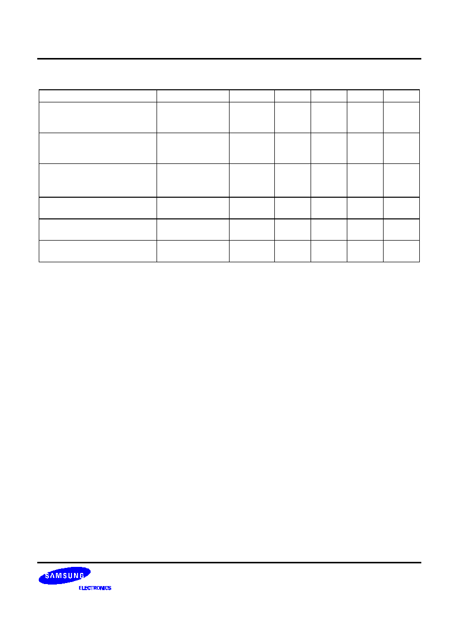
ELECTRICAL CHARACTERISTICS (Continued)
Characteristic
Test Conditions
Symbol
Min
Typ
Max
Units
Tx IF Load resistance
TXIF_OUT,
TXIF_OUT/,
Differential
RIF
-
1
-
k
Tx IF output capacitance
TXIF_OUT,
TXIF_OUT/,
Differential
CIF
-
-
2
pF
Tx IF output impedance
TXIF_OUT,
TXIF_OUT/,
Differential
ZIF
30
-
-
k
VCO input resistance
TX VCO_T1,
TX VCO_T2
RVCO
1.8
2
2.2
k
VCO input capacitance
TX VCO_T1,
TX VCO_T2
CVCO
-
-
1.5
pF
Tx AGC gain control input
impedance
TAGC_CONT
ZAGC
30
80
-
k
S1M8657
TX IF/BBA WITH AGC
8
ELECTRICAL CHARACTERISTICS
Characteristic
Test Conditions
Symbol
Min
Typ
Max
Units
CDMA Performance
Output Center
Freq.
Maximum operating IF frequency
FTR
-
-
300
Mhz
Minimum output
power
Output power when full scale I and Q data
are input to the DAC at minimum AGC gain
MINP
-
-
-83.2
dBm
Maximum output
power
Output power when full scale I and Q data
are input to the DAC at maximum AGC
gain
MAXP
0
-
-
dBm
AGC control
voltage range
Input voltage examination that responds to
the control input when input 15k
resistance is series-connected to the
TAGC_CONT
VCON
0.1
2.4
V
AGC gain slope
Linear control range examination that
measures the gain difference between
control voltages, 1.0V and 2.0V.
G
SLP
33
45
53
dB/V
AGC gain slope
linearity
Examines how far the gain change
between control voltages 1V ≠ 2V is from
the ideal
G
LIN
-3
-
3
dB
In-band spurious
free dynamic
range
Spurious measurement between
±
@1kHz
≠ @630kHz that appears at the IF output
when two in-band 0.5F/S signal are input to
the DAC
I
Spur
35
-
-
dBc
Edge-band
spurious free
dynamic range
Spurious measurement between
±
@630kHz ≠ @1.98MHz that appears at
the IF output when two in-band 0.5F/S
signal are input to the DAC.
E
Spur
35
-
-
dBc
Out-band spurious
free dynamic
range
Spurious measurement above
±
@1.98Mhz
that appears at the IF output when two in-
band 0.5F/S signal are input the DAC
O
Spur
57
-
-
dBc
Carrier feed
through
Examines the carrier feed through when I
and Q single-tone F/S in-band CDMA
spread spectrum data are input.
CF
28
dBc
Spurious free
dynamic range:
IF harmonics
Examines the IF harmonics in the 1.23MHz
range after I and Q single tone F/S data
are input.
E
SFDR
20
-
-
dBc
O
SFDR
9.5
-
-
dBc
SNR, Noise
BAND1
Sets the control voltage so that AGC IF
outputs -83.2dBm ≠ 0.8dBm when I and Q
single tone F/S data are input. Converts
the noise within
±
@100kHz ≠ @1.98MHz
to dBc/Hz.
SNR
1A
104
-
-
dBc/Hz
TX IF/BBA WITH AGC
S1M8657
9
ELECTRICAL CHARACTERISTICS (Continued)
Characteristic
Test Conditions
Symbol
Min
Typ
Max
Units
CDMA Performance
SNR, Noise
BAND2
Sets the control voltage so that AGC IF
outputs -83.2dBm ≠ 0.8dBm when I and Q
single tone F/S data are input. Converts
the noise within
±
@1.98MHz ≠ @44MHz
to dBc/Hz.
SNR
2A
116
-
-
dBc/Hz
ACPR BAND1
Examines the difference between the
power in the @1.23MHz band and the
noise power in the 30kHz band after IS-98
specified CDMA data is input.
ACPR1
52.1
-
-
dB/
30kHz
ACPR BAND2
Examines the difference between the
power in the @1.23MHz band and the
noise power at
±
1.98MHz in the 30kHz
band after IS-98 specified CDMA data is
input.
ACPR2
68.1
-
-
dB/
30kHz
Upper-side-band
Suppression
Examines the I and Q gain and phase
error. Examines the USB suppression ratio
after I and Q single-tone F/S data is input.
USB
25
-
-
dBc
Amplitude flatness
Examines the change in IF amplitude
between @1kHz ≠ @630kHz.
AF
-
-
1
dBpp
Tx puncturing
settling time
Examines the on-off settling time of the TX
block when PAON=Low in the TALK mode.
ST
-
-
6
us
FM Performance
Minimum output
power
Output when full scale data is input to the
DAC at minimum AGC gain.
MIN
PF
-
-
-50
dBm
Maximum output
power
Output when full scale data is input to the
DAC at maximum AGC gain.
MAX
PF
-3
-
-
dBm
AGC control
voltage range
Examines the input voltage responding to
the control input when 15k
resistance is
series-connected to TAGC_CONT.
V
CONT
0.1
V
CC
-
0.1
V
AGC gain slope
Examines the gain difference between
control voltages 1.0 V and 2.0V to examine
the linear control band.
G
SLP
33
45
53
dB/V
AGC gain slope
inearity
Examines if the gain change between
control voltages 1V ≠ 2V is not ideal.
G
LIN
-3
-
3
dB
IF SNR
Noise BAND1
Examines the noise density between
±
@100kHz ≠ @44MHz when single-tone
F/S data is input. This characteristic
generally depends on the VCO phase noise
characteristics.
SNR
F1
110
-
-
dBc/Hz
Maximum
Spurious Content:
Examines the harmonics at the IF when
single -tone F/S data is input.
E
SFDR
20
-
-
dBc
IF harmonics
O
SFDR
9.5
-
-
dBc
S1M8657
TX IF/BBA WITH AGC
10
ELECTRICAL CHARACTERISTICS (Continued)
Characteristic
Test Conditions
Symbol
Min
Typ
Max
Units
SNR, Noise
BAND1
Sets the control voltage so that AGC IF
outputs -83.2dBm ≠ 0.8dBm when I and Q
single tone F/S data are input. Converts
the noise within
±
@100kHz ≠ @1.98MHz
to dBc/Hz.
SNR
1A
104
-
-
dBc/Hz
SNR, Noise
BAND2
Sets the control voltage so that AGC IF
outputs -83.2dBm ≠ 0.8dBm when I and Q
single tone F/S data are input. Converts
the noise within
±
@1.98MHz - @ 44MHz to
dBc/Hz.
SNR
2A
116
-
-
dBc/Hz
ACPR BAND1
Examines the difference between the
power in the @1.23MHz band and the
noise power in the 30kHz band after IS-98
specified CDMA data is input.
ACPR1
52.1
-
-
dB/
30kHz
ACPR BAND2
Examines the difference between the
power in the @1.23MHz band and the
noise power at
±
1.98MHz in the 30kHz
band after IS-98 specified CDMA data is
input.
ACPR2
68.1
-
-
dB/
30kHz
Upper-side-band
Suppression
Examines the I and Q gain and phase
error. Examines the USB suppression ratio
after I and Q single-tone F/S data is input.
USB
25
-
-
dBc
TCXO/VCO/PLL Performance
TCXO input
frequency
f
TCXO
-
19.68
25
MHz
TCXO input level
L
TCXO
-
0.5
2.0
Vpp
Tx VCO frequency
f
TVCO
-
-
500
MHz
Lock mode current
RSET = 39k
LC
14
16
18
uA
Acquisition mode
current
RSET = 39k
AC
140
160
180
uA
Reference spur
Depend on loop bandwidth
RS
-
-
-70
dBc
Max. Acquisition
mode current
RAC
1
-
-
mA
Acquisition to Lock
mode transition
range
WLD
-
-
±
1
kHz
Charge pump
compliance
voltage
Io=16uA
VCHG
0.4
-
V
CC
-
0.4
V
Phase detector
unlock threshold
during FM
ULFM
-
-
12
kHz
TX IF/BBA WITH AGC
S1M8657
11
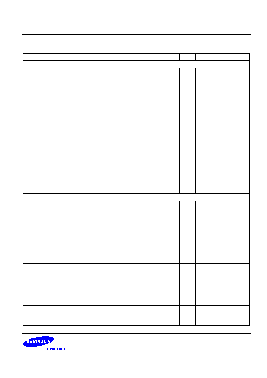
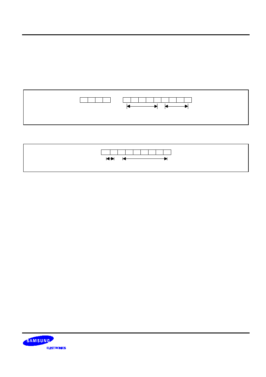
TIMING DIAGRAMS
TCLK Period: 203.4ns
Rising time:
3 -12ns
TCLK
Falling time:
3 - 12ns
Q-DATA
Q-DATA
I-DATA
High time:
101.7ns
Data setup to TCLK transition: 20ns
Data hold after TCLK transition: > 3ns
TCLK to TCLKB Phase delay: < 1.2ns
TCLKB
TXD[7:0]
Low time:
101.7ns
90%
10%
I-DATA
I-DATA
Q-DATA
Figure 1. CDMA Transmit DAC Timing
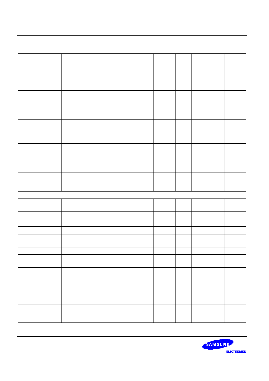
TCLK Period: 8.33us
Rising time:
3 - 12ns
TCLK
Q-DATA
High time:
4.17us
Data setup to TCLK transition: > 20ns
Data hold after TCLK transition: > 3ns
TCLK to TCLKB Phase delay: < 1.2ns
TCLKB
TXD[7:0]
Low time:
4.17us
Falling time:
3 - 12ns
90%
10%
Q-DATA
Q-DATA
Figure 2. FM Transmit DAC Timing
S1M8657
TX IF/BBA WITH AGC
12
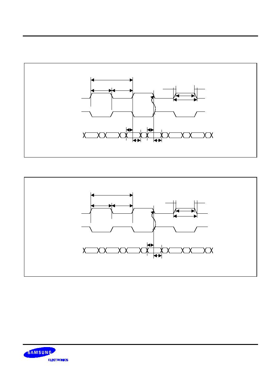
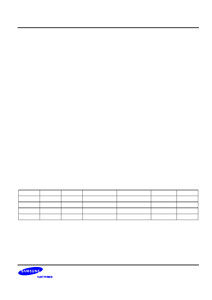
Clock period:
2.44us
Rising time:
3 - 12ns
Falling time:
3 - 12ns
High
time: 1.22us
Low time: 1.22us
GPENA high to conversion end: <40us
D7
D6
D5
D4
D3
D2
D1
D0
GPCLK
GPENA
GPDATA
* All timing specifications is based on
GPCLK=410Khz
GPENA high to
GPCLK: 17us
GPDATA valid before
GPCLK rising edge:
50ns - 780ns
GPDATA valid after GPCLK
falling edge: 50ns
90%
10%
Figure 3. GP-ADC Timing
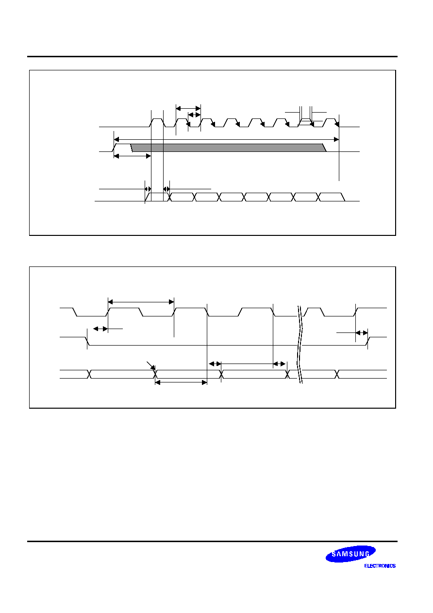
Clock period: 0.6 - 10us
Clock duty cycle: 35 - 65%
CLK
STB
N+1 Data bit set-up time: > 50ns
Valid data bit (N)
DATA line hold time:
50 - 200ns
STB line setup time: 50ns
All data transitions happen while CLK=Low
Clcok N
STB line hold time:
50 - 200ns
DATA
Clcok N+1
Clcok N+2
Valid data bit (N+1)
Valid data bit (N+2)
Figure 4. 3-Line Serial Port Interface Timing

TX IF/BBA WITH AGC
S1M8657
13
Functional Description
S1M8657, a functional block used in Tx signal processing, is located between the RF pre-block and modem. This
product converts the digital I and Q baseband signals sent by the modem to their corresponding analog signals
and moves their frequencies to the IF mid-frequency, where their output levels are controlled. Then, the
differential IF signal is output. Because it has the built-in SPI bus I/F and parallel mode control, it is compatible to
the existing BBA2.0. The programmable Tx PLL is used to generate the precise IF mid-frequency. Here, the
VCO, which oscillates at twice the IF frequency, and QPSK modulator moves the IF frequency from the
baseband. The AGC, connected to the TX IF SAW filter, amplifies or reduces the IF signal level, required by the
CDMA system, at a certain point. Its gain is controlled by the DC voltage in the TAGC_CONT and its output level
range is approx. 90dB. The GP-ADC possessing a switch that can select from three independent inputs is as
system monitor A-D converter, which senses the battery type, remaining battery amount, and temperature.
Various inputs and conditions for this converter can be set via the SPI bus. Moreover, it can use the same BBA
2.0 conditions and parallel control inputs. S1M8657 uses a 0.5um BiCMOS, equipped with high-frequency
bipolar and low power standardized CMOS logic, to operate safely in the low power range, consisting of power
voltage between 2.7V ≠ 3.6V and operating temperature between -30
∞
C ≠ +85
∞
C.
CDMA Transmit Signal Path
S1M8657 is a transmit circuit, installed with PLL, GP-ADC and mode change switch and serial I/F. The transmit
circuit has the Tx AGC, an automatic gain controller, and baseband LPF and D-A converter as well as a VCO
and mixer etc. The CDMA IF output signal is a differential signal modulated to 1.23 MHz spread-spectrum for
CDMA with a normal mid-frequency at 130.38MHz. The mid-frequencies are set based on the time constants of
the components involved with the external VCO and Tx PLL. Tx AGC , connected to both the IF SAW filter and
matching component in the IF-RF converter output located in the RF block, amplifies or reduces the signal
according to the signal size. It takes its orders from the modem chip when it sets the appropriate power level as
required by the CDMA system. Gain is controlled by applying a DC voltage to the TAGC_CONT pin. The applied
DC is produced when the PDM signal, generated as a control signal in the modem, passes through the R-C filter.
The control band of this AGC is approx. 90dB. The QPSK modulator mixes and adds the I-Q baseband signals,
output from the DAC-LPF, with the I-LO and Q-LO signals, respectively, to generate the QPSK signal, which is
sent to the AGC which in turn sends the differential IF to the RF signal processing block. The LO(local oscillator)
signal is generated by the internal oscillating components, externally connected tank coil, and Varactor, and the
externally independent PLL device is used to generate its exact oscillation mid-frequency.
FM Transmit Signal Path
Because the FM modulation in the S1M8657 FM circuit differs entirely from the QPSK, the FM transmit signal
path is very different. The transmit circuit includes an automatic gain controller, Tx AGC, baseband LPF, D-A
converter as well as the VCO and Mixer, which are all the essential blocks as included in the CDMA. The FM
signal is a
±
12kHz modulated signal, with normal mid-frequency of 130.38MHz. These mid-frequencies are
determined by the time constants of the components involved with the external VCO and Tx PLL. Tx AGC ,
connected to both the IF SAW filter and matching component in the IF-RF converter output located in the RF
block, amplifies or reduces the signal according to the signal size. It takes its orders from the modem chip when it
sets the appropriate power level as required by the CDMA system. Gain is controlled by applying a DC voltage
to the TAGC_CONT pin. The applied DC is produced when the PDM signal, generated as a control signal in the
modem, passes through the R-C filter. The control band of this AGC is approx. 90dB. Only the analog Q
baseband signal output by the Q- path DAC-LPF is used in FM modulation and directly connected to the external
Varactor Baseband to change the LO frequency to generate the FM modulation signal. This signal is sent to the
AGC, which sends the differential IF to the RF signal processing block.
S1M8657
TX IF/BBA WITH AGC
14
Serial Port Interface(SPI)
S1M8657 is equipped with the Serial I/F. All internal functions can be controlled through a common bus using an
external controller. The serial I/F can be used by setting pin 31(SEN) high, the pin which permits/ not permit the
SPI. If the SEN becomes low, the SPI cannot be used and the BBA must be used in the existing BBA 2.0 mode.
(All the internal registers are default, which makes the register have the same characteristic as BBA 2.0) Here,
the modem is the master and BBA the slave.
Each pin which uses the SPI bus has the following common functions.
∑
The STB(STROBE) for the serial bus start signal is used to reset serial data transmission.
This pin is used with the IDLEB function in manual mode and designated the IDLB/STB pin.
∑
Serial BUS DATA is used for the bidirection data input /output at serial data transmission.
This pin is used with the FMB function in parallel mode and designated the FMB/DATA pin.
Because it is an open drain type pin, it requires the pull-up resistance of approx. 8k
.
∑
Serial BUS CLK is used to synchronize the data input/output at serial data transmission.
This pin is used with the SLEEPB function in manual mode and designated the SLEEPB/CLK pin.
The SEN(PIN31) pins decide on whether the product will used the SPI bus or parallel control inputs; if is in low,
then the pins the parallel control input functions, IDLEB, FMB, and SLEEPB, but if in high these pins execute the
SPI bus functions, STB, DATA, and CLK. The maximum data transmission (Clock frequency) is 1.53MHz. This
product does not require any external time constants in the internal register because it can use the internal reset
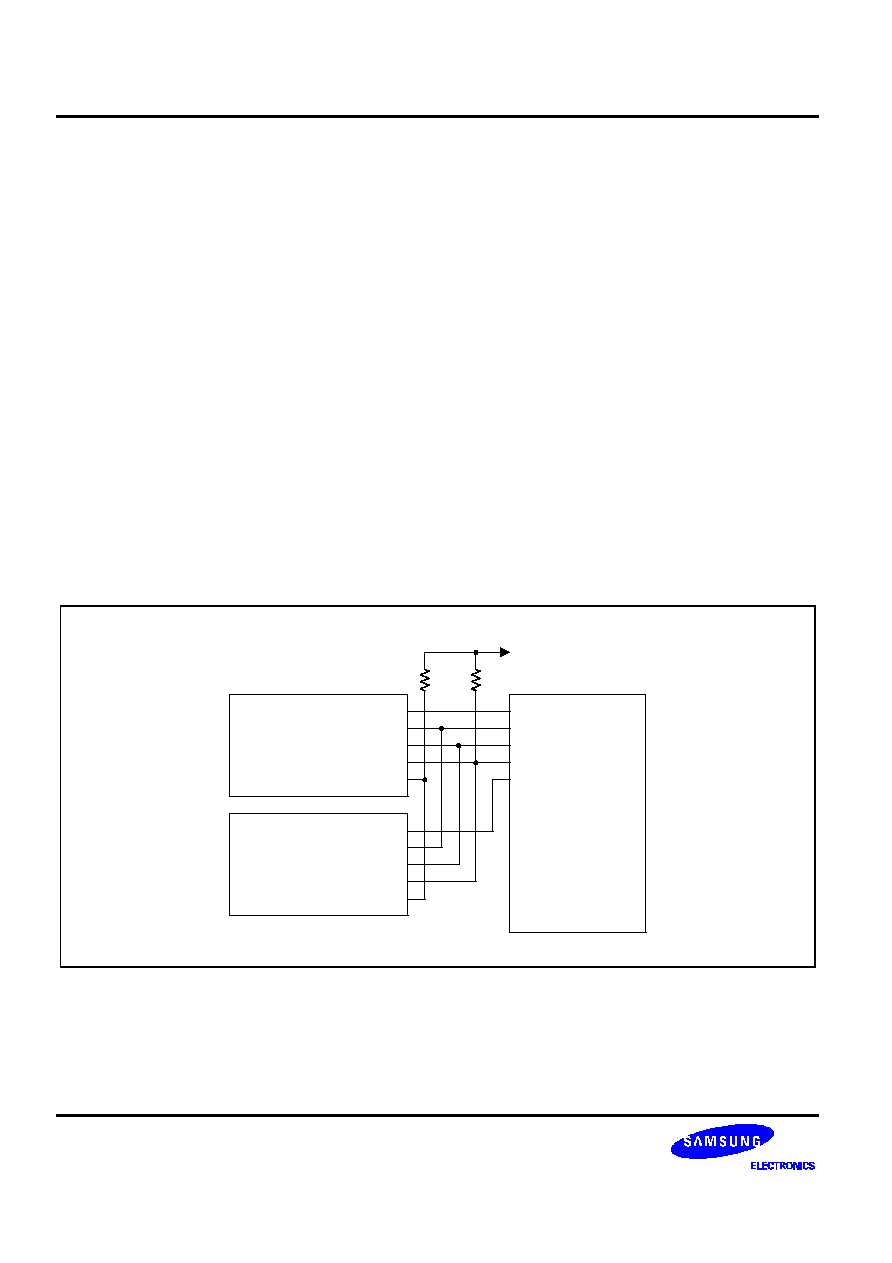
function. Fig. 5 shows the serial connection.
SLOT
STB/IDLEB
CLK/SLEEPB
DATA/FMB
SEN
SMSB/PAON
STB/IDLEB
CLK/SLSB
DATA/FMB
SEN
S1M8656A
S1M8657
SLEEPB
SBST/ADC_ENA
SBCK/ADC_CLK
SBDT/ADC_DATA
PAON
MODEM
V
DD
8k
Figure 5. Serial Bus connection
TX IF/BBA WITH AGC
S1M8657
15
Serial Port Interface Operation
The modem , the master, controls slaves such as S1M8657 using the SPI bus.
The STB falling edge indicates the start of the serial I/F data transmission.
The STB becomes high to mark the end of the data transmission. (Data sent after the STB turns high are not
valid.)
Serial line data is captured and stored as soon as the BBA or the MODEM places the clock on the falling edge.
The SPI 3-line must remain high for at least 1-clock cycle in order to sent new data.
The MSB always outputs the data line data.
After 9-clocks, which is required to send data, the data line driver opens the data line, at which time the data line
becomes high because of the external pull-up resistance.
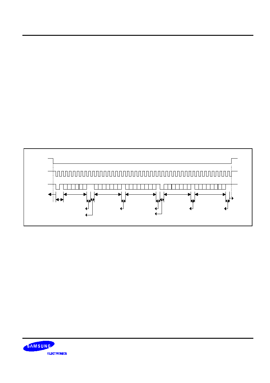
Serial Data Transfer Format
S1M8656A and S1M8657 are all slave devices with the SPI bus. What differentiate them from one another is
their different device IDs. Each company has its own characteristic SPI bus configuration , but normally the 3-line
bus is most often used and sometimes the 2-line bus such as the IIC bus.
Figure 6. shows the serial data transfer format.
mode=01
Dummy
1= Master read
Master drive
Slave Address
Dummy
Master drive
Register Address
Slave Drive
Data
Dummy
0 = Master write
Master drive
Register Address
Master Drive
Data
Dummy
Dummy
End bit
Start bit
STB
CLK
DATA
D5
0 1
D4 D3 D2 D1 D0
D6 D5 D4 D3 D2 D1 D0
D7 D6 D5 D4 D3 D2 D1 D0
D6 D5 D4 D3 D2 D1 D0
D7 D6 D5 D4 D3 D2 D1 D0
Figure 6. Serial Data Transfer Format
(1) The first 2-BITs are for transmission only and this product must send '01'.(Others are not permitted.)
(2) The following 6-bit data specifies the slave device, which is connected to the SPI bus and has its own ID.
(3) The following 1-bit is a dummy bit, which marks the end of the 8-bit data transmission and the beginning of
the next data to be sent.
(4) The following 1-bit decides on whether the master will drive the data line or the slave will. If this bit is '1', the
master will drive , but if '0' the slave will drive the data line.
(5) The following 7-bit data is the register address of the specified slave device; the 7-bits for an address allows
128 register addresses for slaves.
(6) The following high 1-BIT data is a dummy data.
(7) The following 8-BIT data is the data in the device to be driven.
(8) The following 1-BIT data is a dummy data, which marks the end of the 8-bit data transmission and beginning
of the next data to be sent.
(9) The following 1-bit decides on whether the master will drive the data line or the slave will. If this bit is '1', the
master will drive , but if '0' the slave will drive the data line.

S1M8657
TX IF/BBA WITH AGC
16
(10) The following 7-bit data is the register address of the specified slave device.
(11) The following high 1-BIT data is a dummy data.
(12) The following 8-BIT data is the data in the device to be driven.
(Continuos data transmission such as this can be ended with a 1-byte transmission or can be read/written
repeatedly.)
(13) After the last data is sent, the data line opens and becomes high;
(14) CLK continues for half the 1-clock cycle and then becomes high;
(15) STB becomes high as soon as the clock becomes high and this marks the end of data transmission.
TX IF/BBA WITH AGC
S1M8657
17
Modes of Operation
S1M8657 can be controlled by parallel control mode or by SPI bus. The analog switch , an existing external
component, in the IC an be also controlled through separate specified parallel inputs or by SPI. The modes of
operation can be formed by parallel inputs such as FMB, IDLEB, and PAON, or by related SPI registers, as
shown in Table 1.
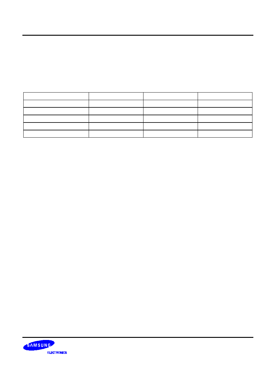
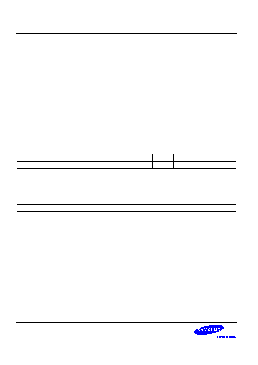
Table 1. Mode control in the parallel mode control
MODE
FMB
IDLEB
PAON
CDMA talk
H
H
H
CDMA idle
H
L
X
FM talk
L
H
H
FM idle
L
L
X
Tx puncture (SPI Only)
X
H
L
The modem in CDMA transmit mode operates the I and Q DAC in S1M8657, which then outputs the CDMA
spread-spectrum with Tx IF mid-frequency. All the circuits in S1M8657 are stopped in CDMA receive mode (Idle).
The modem only operates Q-DAC in the FM transmit mode (Talk). Besides this, all CDMA related circuits are
stopped. The signal for FM modulation passes through the Q-FM-LPF (FM-MOD) output pin to come out.
All
circuits in S1M8657 are stopped in FM receive only mode (Idle). Because Tx puncture mode can only be
controlled through the SPI bus, it turns on and off the blocks related to the intervals with no data. By doing so, it
minimizes the consumption current. The SPI registers related to this feature are controlled by setting PAON =
Low, SEN = High, IDLEB = High.
Tx Phase Locked Loop
S1M8657 has a built-in programmable PLL which can determine the IF mid-frequency. If the SPI BUS is not
used, the default value in the built-in register must be used; the Tx IF frequency is 130.38Mhz when TCXO =
19.68Mhz. The block diagram of the PLL is shown in Figure 7. The PLL is composed of the VCO, R-Divider, N-
Divider, and Phase Detector, while the Loop filter and VCO components are outside S1M8657. The divide ratios
in the PLL R and N counters can be programmed through the SPI bus. These can change the phase comparison
frequency. The N-Counter is composed of a 9-BIT A-Counter and 4-BIT B-Counter and 8/9 or 16/17 Dual-
Modulus Prescaler.
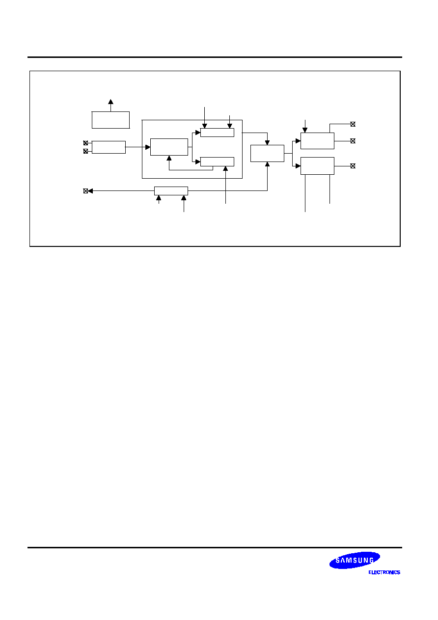
S1M8657
TX IF/BBA WITH AGC
18
PLLR0[7:0]
PLLR1[1:0]
PLLN0[3:0]
PLLN0[7:4]
PLLN1[4:0]
PLL_MODE[6]
PLLR1[7:5]
PLL_MODE[4:3]
N Counter
to Mixer
TX_VCO_T1
TX_VCO_T2
TCXO
PDISET
PDOUT
LOCK
Divide
by 2
TX VCO
Prescaler
P or P+1
A-Counter
B-Counter
Phase
detector
R-Counter
Lock
detector
Charge
pump
Figure 7. Tx PLL Synthesizer Block Diagram
TX IF/BBA WITH AGC
S1M8657
19
The A and B-Counter divide ratios can be changed by programming the PLLNO and PLLN1 among the SPI
registers. They pass through the VCO internal output, TXVCO_OUT, and are input to the prescaler, and the
prescaler outputs are input to A and B-counters. If the B-Counter is not "0", the Prescaler divides by P+1(division
ratio of 9 or 17 ); if B-Counter is "0", the Prescaler divides by P(division ratio 8 or 16). If A-Counter becomes "0",
N-Counter is reset. If A-Counter output becomes fv, this becomes the comparison input for the PD (phase
comparator). R-Counter can be changed by programming PLLR0 and PLLR1 of the SPI registers. As a 10-bit
divider, R-Counter divides TCXO, which is then used as the reference input for the PD.
9- bit A-counter
PLLN1[4:0]
PLLN0[7:4]
PLLN0[3:0]
4-bit B-counter
MSB
LSB
Figure 8. Map of N Counter
PLLR0[7:0]
PLLR1[1:0]
MSB
LSB
Figure 9. Map of R Counter
The N-counter divide ratio (N) changes according to the prescaler value and is determined by the following
equation.
N = P
◊
A + B, where A
512, 0
B
(P-1), and B < A.
The prescaler can use PLLN1[7] to select from either 8/9 or 16/17, the reference value being 16/17. If this bit
becomes "0", 8/9 is chosen as the prescaler divide ratio. N-Counter, composed of the 9-BIT A-Counter and 4BIT
B-Counter, lowers the VCO frequency and sends it to the PD.
PLL equation : N-Counter divide ratio N = f
VCO
/f
PD
A-Counter divide ratio A = Int(N/P), A
512.
The value of A written into PLLN1 and PLLN0 as shown in Figure 8 is a binary value for A-1. For example, the
reference values, PLLN1[4:0]=00000 and PLLN0[7:4]=1100, are decimal, 12, and A is for 13.
The B-counter can be programmed with PLLN0[3:0].
B = N - P
◊
A, 0
B
15, P=16
The reference value for A and B-Counter (A=13, B=4) makes the VCO oscillating frequency equal to 260.76 MHz
when TCXO is at 19.68MHz, and PD phase comparison frequency becomes 1.23MHz.
The 10-bit R-counter can be programmed using the SPI registers, PLLR0 and PLLR1.
The R-Counter makes the f
R
input signal for PD based on the TCXO reference signal.
R-Counter divide ratio R = f
REF
/f
PD
The R-counter value set based on PLLR0 and PLLR1 is for R-1; for example, when PLLR0 = 00001111 and
PLLR1=00, decimal value is 15, but it is R-1, real value R is 16.

S1M8657
TX IF/BBA WITH AGC
20
[Order of divide ratio calculation]
VCO = 260.76MHz, TCXO = 19.68MHz, Phase detect frequency = 1.23MHz, Prescaler = 16
1) Determine the value of N : N = f
VCO
/f
PD
= 260.76MHz/1.23MHz = 212
2) Determine the value of A : A = Int(N/P) = Int(212/16) = 13
When this value is set in the register, the value of A-1(12) must be placed.
Binary value is 000001100.
3) Determine the value of B : B = N - P
◊
A = 121 - 16
◊
13 = 4
4) Determine the value of R : R = f
REF
/f
PD
= 19.68MHz/1.23MHz = 16
The R register value is R-1 so 15 must be written. Binary value is 0000001111.
The external PDISET resistance determines the charge pump from PDOUT. This resistance determines the
current flowing between PDISET and GND as follows.
Io = Rset/0.64V
Io is the charge-pump current when the PLL is locked. If the resistance is 39k
, Io becomes 16uA.
The charge-pump current is classified into lock mode current and acquisition mode current to quickly stabilize the
un-locked IC. The charge-pump current of the acquistion mode flows 10 times faster than that of the lock mode,
thus providing faster stability. Although the Lock-Acquisition current can be changed from one to the other, the
SPI PLL_Mode [4:3] register value can be used to permanently set the charge-pump current as either acquisition
mode current or lock mode current. However, the type of current to be set should be carefully decided based on
the amount of surrounding noise flowing into VCO. The charge-pump polarity can be change with PLLR1[4] to
respond to the various conditions of the capacitor, whose value can be changed "+' or "-" for the varactor signal,
according to how the VCO is used. A lock pin has been prepared to indicate that lock has occurred because the
Tx frequency has entered the set band. This pin can be used to select from either the open-drain output or CMOS
output. If the OPEN_DRAIN output is selected, an external 10k
Pull up resistance is required. PLL_MODE[6]
can be set to select the output type. Lock -unlock states can be determined by counting how many times the
phase difference between the signal in the IC and the reference signal matches within the set phase difference
band. Two criteria which can be used to detemine the lock are the phase difference band and the frequency of
phase match during a set period. Here the user can select the frequency of phase match, the purpose of which is
to determine whether or not the lock is a stable lock or a temporary lock condition. Namely, the lock condition
,when there are many phase matches, is a very stable condition, but it requires time. The phase difference here
refers to the phase difference between the N-counter output fv and R-counter output f
R
. Whether or not to cancel
the lock condition can be decided by determining how many times 2 phase differences fall within the set range
within a specified duration. PLLR1[7:5] SPI register is used to set the phase match or unmatch frequency limit.
Here , this limit is called the Lock-length, which is determined as follows:
f
R
is the reference frequency in the phase comparator.
f
R
= f
TCXO
/R, f
TCXO
is the basic TCXO frequency, R is the divide ratio for the basic TCXO frequency(R-Counter)
fv is the VCO dividing frequency which is compared to the reference frequency in the phase comparator.
fv = (f
VCO
+ f
ERROR
)/N, where f
VCO
is the VCO basic frequency and f
ERROR
is the allowable maximum frequency
range.
Based on the above equation, the number of PD pulses required for the VCO frequency
in a set band is
N
PD
= 2
◊
T
TCXO
/(1/f
R
- 1/f
V
), T
TCXO
is the period of the TCXO basic frequency.
The number of TCXO pulses for the VCO frequency in a set range is
N
TCXO
= R
◊
N
PD
where, Lock-length M = log
2
(N
TCXO
) - 13
Lock counter length is 2
(M+13)
.
TX IF/BBA WITH AGC
S1M8657
21
The M in binary can be set by changing the PLLR1[7:5] register value. And normally, f
ERROR
is designed to the
limit of 1kHz.
[An example of a Lock length design ]
f
VCO
= 260.76MHz; f
TCXO
= 19.68MHz; f
ERROR
= 1kHz; R = 16, N = 212
f
R
= f
TCXO
/R = 19.68MHz/16 = 1.23MHz
fv = (f
VCO
+ f
ERROR
)/N = 1230004.71698
N
PD
= 2
◊
T
TCXO
/(1/f
R
- 1/fv) = 32600
N
TCXO
= R
◊
N
PD
= 16
◊
32600 = 521600
M = Roundup{log
2
(N
TCXO
)} - 13 = Roundup(18.9926) - 13 = 6
Therefore. Lock detector length is 2
19
TCXO
.
General Purpose ADC
The GP-ADC for the system monitor has a built-in 3-input switch Serial 8-BIT A-D Converter and is used
generally used to sense the temperature, and battery amount and type. The GP-ADC can be controlled by the
following methods.
Parallel control as in the existing S1M8653B when the SPI is not used and SEN = low.
GPENA, GPDATA, and GPCLK must be used.
Basic and enhanced modes exist with SPI use when SEN = High
: Controlled through the SPI register and GPENA in the Basic Mode(TXMODE_CONT[0] = Low),
and can output through either the SPI register or GPDATA and GPCLK pins.
: Controlled according to the contents in the GPADC_MODE[7:0] in the Enhanced
Mode(TXMODE_CONT[0] = High).
General Purpose ADC Operation without SPI (SEN = low)
When SEN = low, the Serial BUS(SPI BUS) is not used. In such a case, GP-ADC is controlled through SLSB,
SMSB, GPENA, GPDATA and GPCLK provided from external pins or data must be sent. Under these
conditions, the GP-ADC is reset at the rising edge of GPENA from the modem and starts the conversion. The
converted digital code is synchronized to the continuous 9 GPCLK and sent to the modem. To start a new GP-
ADC conversion, GPENA must be at Low. Input range or signal are selected based on the SMSB/PAON and
SLSB/CLK states, as shown in Table 2.
Table 2. Input and Range Select (SEN = low)
SMSB
SLSB
GPIN
Vin MID
Input Range
LSB/Step
Zin
0
0
GPIN1
0.75V
0.5V
2mV
0
1
GPIN1
1.5V
2V
8mV
1
0
GPIN2
1.5V
2V
8mV
1
1
GPIN3
1.5V
2V
8mV
S1M8657
TX IF/BBA WITH AGC
22
General Purpose ADC Enhanced-Mode Operation Using SPI
(SEN = high, TXMODE_CONT[0] = high)
When SEN = High the SPI BUS can be used. The GP-ADC operates in the basic mode or enhanced mode. If the
TXMODE_CONT[0] is "1", it operates in the enhanced mode and the SPI registers control the input selection,
clock frequency and input range. The basic setting is the Basic Mode.
If TXMODE_CONT[0] = "1" in the basic mode, the GP-ADC operates in the enhanced mode. If all GP-ADC
related controls and input/output function are conducted through the SPI bus, the GP-ADC only outputs the SPI
input/output. GPENA can also drive GP-ADC; in this case, GPDATA and GPCLK are output and save at the
same time in the SPI register, GPADC_RSLT[7:0], except that nothing can be input to the input select pins ,
SMSB/PAON and SLSB/CLK. It's simpler to think that in this mode the SPI registers perform the roles of what the
parallel control pins did in the existing S1M8653B If GPENA and TXMODE_CONT[7] = High, GP-ADC starts the
conversion. Moreover, for a new conversion, GPENA and TXMODE_CONT[7] must be left at Low, and restart
begins at the rising edge of when they become high. While conversion is going on, GP-ADC cannot receive any
signals. GPADC_RSLT[7:0], which has the GP-ADC conversion value, maintains its previous value until the end
of the new conversion.
Table 3. Enhanced-Mode Register Definition
GP MODE
CLOCK Divide Ratio
Input Range
Input Select
GPADC_MODE[7:0]
D7
D6
D5
D4
D3
D2
D1
D0
Default
1
0
0
1
0
0
0
0
Table 4. Enhanced-Mode Analog MUX
GPADC_MODE[1:0]
Input Select
GPADC_MODE[1:0]
Input Select
00
GPIN1
10
GPIN2
01
Reserved
11
GPIN3
TX IF/BBA WITH AGC
S1M8657
23
Table 5. Enhanced-Mode Input Range Selection
GPADCV[5:2]
Vin(Mid)
Input Range
LSB mV/Step
Zin
0000
1.0V
1V
4
0001
2.0V
1V
4
0010
1.5V
2V
8
0011
1.5V
2V
8
0100
0.75V
0.5V
2
0101
1.5V
2V
8
0110
1.5V
2V
8
0111
1.5V
2V
8
1000
0.5V
1V
4
1001
1.0V
2V
8
1010
1.25V
0.5V
2
1011
1.5V
1V
4
1100
2.0V
2V
8
1101
1.5V
0.5V
2
1110
1.75V
0.5V
2
1111
2.0V
0.5V
2
GP-ADC Enhanced Mode inputs are shown in Table 5. The IC input impedance is always kept high to reduce the
loading effect of the input impedance. However, if the external input divider impedance is very large, the
parasitic capacitor cannot charge or discharge quickly enough, generating a high speed conversion error.
Therefore, it is best to use a low resistance at the input terminal. The LSB step is the difference between the
input voltages that generate two codes, respectively. This is shown in Table 5. The GP-ADC needs the clock for
conversion. This clock self-divides and uses TCXO and influences the conversion time. Although a 412kHz clock
was used in S1M8653B, this IC can select from clock speeds between 308kHz ≠ 1.23 MHz, as shown in Table 6,
according to the contents in SPI register GPADC_MODE[6:7]. The recommended clock speed is between
410kHz ≠ 615kHz.
Table 6. GP-ADC Clock Divide Ratio
GPADC_MODE[7:6]
Clock Divide Ratio
System Clock(TCXO = 19.68MHz)
00
16
1.23MHz
01
32
615kHz
10
48
410kHz
11
64
308kHz
S1M8657
TX IF/BBA WITH AGC
24
General Purpose ADC Basic-Mode Operation Using SPI
(SEN = high, TXMODE_CONT[0] = low)
SPI can be used when SEN= high. The GP-ADC operates in the basic mode. Under these circumstances, GP-
ADC is under the control of the SPI registers. The results of conversion can be output to not only the SPI register
GPADC_RSLT[7:0] but also to GPDATA and GPCLK. When the basic mode turns on and SPI starts, they are
automatically set. If the TXMODE_CONT[0] is "0" and all GP-ADC related controls and input/output function are
conducted through the SPI bus, the GP-ADC only outputs the SPI input/output. GPENA can also drive GP-ADC;
in this case, GPDATA and GPCLK are output and save at the same time in the SPI register, GPADC_RSLT[7:0].
In this mode, MODE_CONT[6:5] register holds the parallel input pins, SMSB/PAON and SLSB/CLK. If GPENA
changes from low to high or GPDAC_MODE[7] register from "0" to "1", the GP-ADC stars the conversion.
Essentially these indicate the start of conversion in basic mode. For a new conversion, these GPENA and
GDAC_MODE[7] must be left at low state and intialization starts at the rising edge of when they become high.
While conversion is going on, GP-ADC cannot receive any signals. GPADC_RSLT[7:0], which has the GP-ADC
conversion value, maintains its previous value until the end of the new conversion.
Table 7. GP-ADC Range Select in Basic Mode
GPADC_MODE[4]
TXNODE_CONT[6:5]
Vin Mid
Input Range
LSB(mV)
GPADC Input
Zin
0
00
1.0
1.0
4
GPIN1
0
01
2.0
1.0
4
GPIN1
0
10
1.5
2.0
8
GPIN2
0
11
1.5
2.0
8
GPIN3
1
00
0.75
0.5
2
GPIN1
1
01
1.5
2.0
8
GPIN1
1
10
1.5
2.0
8
GPIN2
1
11
1.5
2.0
8
GPIN3
GP-ADC can select from various input range as well as resolution value for each mid-voltage and LSB. It has a
built-in input switch, which allows for easy connection with the input sensor. All programmable options are set by
SPI registers TXMODE_CONT[6:5] and GOADC_MODE[4].
General Purpose ADC Conversion Time
GP-ADC conversion time is determined based on the TCXO and GP-ADC clock divide ratio in the SPI register
GPADC_MODE[7:6]. GP-ADC needs a total of 6 GPCLK cycles from its restart to start of data sampling; the
required ADC conversion time is 8 and 1/2 GPCLK cycles.
A total of 14.5 GPCLK cycles are used.
Table 8. Maximum Conversion Time
GPADC_MODE[7:6]
Units
00
01
10
11
TCXO frequency
MHz
19.68
19.68
19.68
19.68
Divide ratio
16
32
48
64
Conversion time
us, max
11.79
23.58
35.37
47.17
TX IF/BBA WITH AGC
S1M8657
25
CONTROL REGISTERS
Register name
Address
R/W
Default vale
Description
RESET
0x00
W
-
Reset.
Resets S1M8657 and all the register values are
returned to their original value.
SPI_ID
0x01
R
0x2A
SPI_ID.
All slaves have an independent ID, which is
used to distinguish the devices connected to the
SPI bus and to send data to the desired device.
PLLN0
0x02
R/W
0xC4
PLLN0.
Determines the divide ratio needed in the PLL
divider.
PLLN1
0x03
R/W
0x80
PLLN1.
Determines the divide ratio needed in the PLL
divider.
PLLR0
0x04
R/W
0x0F
PLLR0.
Determines the divide ratio needed in the PLL
divider.
PLLR1
0x05
R/W
0xD0
PLLR1.
Determines the divide ratio needed in the PLL
divider.
PLL_MODE
0x06
R/W
0x00
PLL_MODE
not applied
0x07
not used
not applied
0x08
not used
not applied
0x09
not used
TXMODE_CTL
0x0A
R/W
0x02
TXMODE_CTL Sets the transmission mode
GPADC_RESULT
0x0B
R
-
GPADC_RESULT GP-DATA storage.
GPADC_MODE
0x0C
R/W
0x90
GPADC_MODE Sets the GP-ADC.
ON_OFF
0x0E
R/W
0x08
ON_OFF
Decides on whether to operate the functional
block to be used in Tx puncture. To use this
register, PAON must be low and Talk mode
must be in place.
Reserved
0x10
Absolutely not used.
Reserved
0x11
Absolutely not used.
S1M8657
TX IF/BBA WITH AGC
26
DESCRIPTION OF REGISTER
ADDRESS
NAME
TYPE
BITS
Description
00
RESET
W
-
This is used like a command and if this address is accessed, all
register values are restored to their original set value.
01
SPI_ID
R
[5:0]
This ID number must be used to use the registers as S1M8657
in this IC. SPI_ID = 2Ah
02
PLLN0 [7:0]
R/W
[7:4]
PLLAC[3:0]. Default = 1100.
Refers to the lower 4-bit in the 9-BIT A-Counter. Remember that
the total 9-BIT value refers to the A-1 value.
[3:0]
PLLBC[3:0]. Default = 0100.
Register that sets the 4-BIT B-Counter.
03
PLLN1 [7:0]
R/W
[7]
PSC_MODE, Default = 1. Sets the Prescaler Dual Mode.
1: P = 16 Mode, with divide ratio of 16 or 17.
0: P = 8 Mode, with divide ratio of 8 or 9.
[6:5]
Default = 00
Absolutely not used.
[4:0]
PLLAC[8:4]. Default = 00000.
Refers to the upper 5-bit in the 9-BIT A-Counter. Remember that
the total 9-BIT value refers to the A-1 value.
04
PLLR0 [7:0]
R/W
[7:0]
PLLRC[7:0]. Default = 00001111.
Refers to the lower 8-bit in the 10-BIT A-Counter. Remember
that the total 10-BIT value refers to the A-1 value.
05
PLLR1 [7:0]
R/W
[7:5]
LOCK_LEN. Default = 110.
Lock output set register sets the lock output by detemining the
time cut-line for level of PLL & VCO stabilization Phases must
match duringTCXO*2
(M+13)
for lock.
[4]
PD_MODE. Default = 1
Decides the polarity of the phase comparator gain (+ or -1).
0: Negative VCO gain (-Kv)
1: Normal operation.
[3:2]
Default = 00, Absolutely not used.
[1:0]
PLLRC[9:8]. Default = 00.
Refers to the upper 2-bit in the 10-BIT R-Counter. Remember
that the total 10-BIT value refers to the R-1 value.
06
PLL_MODE
R/W
[7]
Default = 0. Absolutely not used.
[6]
LOCK_MODE. Default = 0.
Assigns the lock output form, the lock detector output.
1: Standard CMOS output
0: Requires an external pull up register because of the open
drain output.
[5]
Default = 0
Absolutely not used.
TX IF/BBA WITH AGC
S1M8657
27
DESCRIPTION OF REGISTER (Continued)
ADDRESS
NAME
TYPE
BITS
Description
[4:3]
CHG_PMP. Default = 00. Sets the Charge-pump Mode.
00: Normal operation( Separates the current amount for
Lock- Aquisition Mode.)
01: not used
10: Always operates it with 10x Acquisition current.
11: Always operates it with 1x Lock current.
[2:0]
Default = 000, Reserved
0A
TXMODE_
CONT [7:0]
R/W
[7]
GPADC_ON. Default = 0.
GP-ADC conversion start command register. This bit must be
on stand-by as "0" to start a new conversion.
1: Resets GPADC and starts conversion.
0: GPADC conversion stand-by.
[6]
GP_SMSB. Default = 0
Upper 1-bit of the 2-bit input for selecting input switch.
1: SMSB is "1".
0: SMSB is "0".
[5]
GP_SLSB. Default = 0
Lower 1-bit of the 2-bit input for selecting the input switch.
1: SLSB is "1".
0: SLSB is "0".
[4]
CDMA_MODE. Default = 0(FM)
Replaces the existing FMB pin function.
1: Sets CDMA Mode.
0: Sets FM Mode.
[3]
IDLE_MODE. Default = 0(IDLE)
Replaces the existing IDLEB pin function.
1: Talk Mode.
0: Idle Mode.
[2]
Default = 0, Not used.
[1]
Default = 1, Not used.
[0]
GPENH. Default = 0
Select bit for enhanced mode or basic mode in the GP-ADC
Mode
1: GPADC is set to Enhanced Mode.
0: GPADC is set to Basic Mode.
0B
GPADC_RSLT
R
[7:0]
Saves the most recent conversion value as read-only.
S1M8657
TX IF/BBA WITH AGC
28
DESCRIPTION OF REGISTER (Continued)
ADDRESS
NAME
TYPE
BITS
Description
0C
GPADC_MODE
R/W
[7:6]
GPADC_CLK. Default = 10.
Sets the internal clock divide ratio for GP-ADC conversion.
00: TCXO/16, GPADC Clock=1.23MHz with TCXO=19.68MHz
01: TCXO/32, GPADC Clock=615kHz with TCXO=19.68MHz
10: TCXO/48, GPADC Clock=410kHz with TCXO=19.68MHz
11: TCXO/64, GPADC Clock=308kHz with TCXO=19.68MHz
[5:2]
GPADC_RAN. Default = 0100
GP-ADC input range and precision selection.
(TXMODE_CONT[0] = 0)
[1:0]
GPADC_IN. Default = 00. Selects one of the 3-inputs.
00: IN1, 01: not used, 10: IN2, 11: IN3
GPADCV[5:2]
Vin Mid
Input Range
LSB Mv/Step
Zin
0000
1.0
1
4
0001
2.0
1
4
0010
1.5
2
8
0011
1.5
2
8
0100
0.75
0.5
2
0101
1.5
2
8
0110
1.5
2
8
0111
1.5
2
8
1000
0.5
1
4
1001
1.0
2
8
1010
1.25
0.5
2
1011
1.5
1
4
1100
2.0
2
8
1101
1.5
0.5
2
1110
1.75
0.5
2
1111
2.0
0.5
2
TX IF/BBA WITH AGC
S1M8657
29
DESCRIPTION OF REGISTER(Continued)
ADDRESS
NAME
TYPE
BITS
Description
0E
TX_PWR
R/W
[7]
TXDAC_PWR. Default = 0
Stops the TX-DAC.
1: TXDAC stop.
0: TXDAC operation.
This register is
valid only when
the PAON pin is
at low.
[6]
TXFLT_PWR. Default = 0
Stops TX-CDMA/FM Filter.
1: TX filter stop.
0: TX filter operate.
[5]
UPMIX_PWR. Default = 0
Stops TX-VCO, Mixer, and Quad_gen.
*Advantageous in terms of set-up time when not used.
1: TX VCO, Mixer, and Quad_gen stop.
0: TX VCO, Mixer, and Quad_gen operate.
[4]
TXAGC_PWR. Default = 0
Stops TX-AGC.
1: TXAGC stop.
0: TXAGC operate.
[3]
TXPATH_PWR. Default = 1
Stops TX-AGC.
1: TXAGC stop.
0: TXAGC operate.
[2]
TXPLL_PWR. Default = 0
Stops the PLL.
*Do not use when there is a problem with set-up time.
1: TX_PLL stop.
0: TX_PLL operate.
[1]
TXMIX_PWR. Default = 0
Stops TX-Mixer and Quad_gen.
*Recommend using this bit rather than UPMIX_PWR bit.
1: TX Mixer and Quad_gen stop.
0: TX Mixer and Quad_gen operate.
[0]
Not used.
When IDLEB = Low, minimum bias current is maintained by stopping all the TX circuit functions. To use the
above Tx Puncture function, the external control pin PAON must be at low, and the IDLEB register bit must be at
high. If PAON is High, it does not respond to the PX_PWR register contents.
S1M8657
TX IF/BBA WITH AGC
30
GRAPH
10
100
1K
10K
100K
1M
-120
Phase noise(dBc/Hz)
-110
-100
-90
-80
-70
-60
-50
-40
-30
Frequency offset(Hz)
GRPH 3-1 S1M8657X01 VCO Open Loop Phase Noise
Vcntl(V)
0
-20
-60
-80
-100
-40
0.0
0.5
1.0
1.5
2.0
2.5
3.0
Output Power(dBm)
75
65
55
45
35
25
Rs=3.3K
ACPR2
Po
ACPR1
for CDMA full-scale input.
GRPH 3-2 S1M8657X01 Output Power, ACPR vs. Vcntl Performance
GRPH 3-1 S1M8657 VCO Open Loop Phase Noise
GRPH 3-2 S1M8657 Output Power, ACPR vs. Vcntl
Performance for CDMA full-scale Input
for CDMA full-scale input.
-25
0
+25
+50
+75
-50
+100
Temperture(C)
Output Variation(dB)
-1
0
+1
Rs=3.3K/Po=-6dBm
GRPH 3-3 S1M8657X01 Output Variation vs. Temperature
Rs=3.3K/PDM=3.3V
-10
-20
-30
-40
-50
-80
-70
-60
SNR BAND-1(dBc/Hz)
115
105
95
85
75
65
55
45
0
Lower sideband Power(dBm)
GRPH 3-4 S1M8657X01 CDMA SNR BAND-1 vs. Lower sideband Pout.
GRPH 3-3 S1M8657 Output Variation vs. Temperature
for CDMA full-scale Input
GRPH 3-4 S1M8657 CDMA SNR BAND-1 vs. Lower
sideband Pout.
TX IF/BBA WITH AGC
S1M8657
31
-10
-20
-30
-40
-50
-80
-70
-60
115
0
110
105
100
95
90
85
80
Rs=3.3K/PDM=3.3V
SNR-1(dB)
Output Power(dBm)
GRPH 3-6 S1M8657X01 CDMA SNR BAND-1, 1.98M to 44Mhz offset.
-10
-20
-30
-40
-50
-80
-70
-60
115
0
110
105
100
95
90
85
80
Rs=3.3K/PDM=3.3V
SNR-1(dB)
Output Power(dBm)
GRPH 3-5 S1M8657X01 CDMA SNR BAND-1, 100K to 1.98Mhz offset.
GRPH 3-6 S1M8657 CDMA SNR BAND-1, 1.98M to
44MHz offset
GRPH 3-5 S1M8657 CDMA SNR BAND-1, 100K to
1.98MHz offset
S1M8657
TX IF/BBA WITH AGC
32
TEST CIRCUIT
35
36
33
34
31
32
29
30
27
28
25
26
2
1
4
3
6
5
8
7
10
9
12
11
14
13
16
15
18
17
20
19
22
21
24
23
47
48
45
46
43
44
41
42
39
40
37
38
S1M8657
VCC
10nF10nF
10nF
10nF
1nF
1nF
VCOIN
TCLK
GPCLK
GPDATA
GPENA
IN1
IN2
IN3
TPLL
SW_GP
GPIN
SW_MSB
R=22K
SW_SEN
SW_FM
SW_IDL
SW_LSB
CLK
STB
DATA
SPI_PORT
1nF
TLOCK
TCXOIN
10K
TPDSET
SW_PDST
10K
39K
TPDO
10nF
TFMOD
1nF
10K
1SV229
10K
10K
10K
1.8K
VCEN
SW_PDO
2.2uF
0.033uF
4pF
47pF
TVCO
10nF
10nF
1nF
1:8
7pF
7pF
1K
1nF
2.3nH
1uF
0.5K
3.3uH
0.5K
3.3uH
10nF
47pF
TIF_MON
SW_VCO
TXD7
TXD6
TXD5
TXD4
TXD3
TXD2
TXD1
TXD0
TCLKB
TX IF/BBA WITH AGC
S1M8657
33
48BCC PKG OUTLINE
7.00
+
0.10
0.085°æ0.040
Stan off
0.80 MAX
Total height
SIDE VIEW
#1 INDEX LASER MARK
TOP VIEW
#1
#13
#25
#37
7.00 + 0.10
7.00
+
0.10
#13
#25
#37
#1
C0.2
0.40 + 0.10
0.50 TYP
0.30 + 0.10
0.045 + 0.10
0.045 + 0.10
0.045 + 0.10
0.045 + 0.10
6.15 TYP
6.15 TYP
6.15 TYP
5.0 TYP
BOTTOM VIEW
5.0 TYP
6.15 TYP
S1M8657
TX IF/BBA WITH AGC
34
PKG DIMENSION
48LQFP PKG OUTLINE
#48
7.00
+ 0.20
9.00
+ 0.30
7.00
+
0.20
9.00
+
0.30
0.10 MAX
0.127
+ 0.10
- 0.05
0-8
NOTE: Dimensions are in millimeters.
#1
0.18
+ 0.10
- 0.05
0.50
0.08 MAX
(0.75)
0.50 - 0.20
0.05 MIN
1.40
+ 0.10
1.60 MAX